1. Introduction
Zinc oxide (ZnO) is a direct group II–VI binary compound semiconductor with a wide energy bandgap of 3.37 eV, which is similar to that of gallium nitride (GaN). It has a larger exciton binding energy of 60 meV at room temperature, allowing efficient and stable excitonic emission against thermal dissociation for ultraviolet (UV) light-emitting diode (LED) and laser diode application. Compared to the complicated and hazardous dry etching process for patterning GaN material in device fabrication, patterned ZnO is achievable by the common wet etching process, since it is very sensitive to most acids, such as hydrochloric acid. Accordingly, ZnO material is expected to be more promising than the current mainstream GaN-based device for short-wavelength optoelectronic applications [
1,
2,
3,
4]. Additionally, the growth in technology and temperature necessary to realize a ZnO film with quality
c-axis crystallization is much simpler, such as when done by sputtering, pulse laser deposition, and hydrothermal methods, rather than for the epitaxial GaN layer, resulting in potentially low-cost fabrications and processes for ZnO-based devices [
5,
6,
7,
8]. Among these deposition methods, sputtering technology is a commercially used method for preparing large-area and cost-efficient polycrystalline ZnO layers on various substrates in applications for optoelectronic devices at a relatively low temperature. However, the ion-bombardment damage from the sputtering deposition always caused the resulting ZnO film to diverge from stoichiometry, which was mainly attributed to a deficiency in oxygen atoms. Moreover, the quality of the ZnO film was closely connected with the substrate materials. Accordingly, intermediate layers such as TiO
2, Al
2O
3, Cr
2O
3, Lu
2O
3, AlN, and Ti—which were prepared prior to ZnO film deposition to facilitate the crystalline growth as well as an additive post-annealing treatment on the ZnO film for re-crystallization—were reported to improve the sputtered ZnO film with fewer native defects [
9,
10,
11,
12,
13,
14,
15,
16]. For instance, Zhang et al. reported a SiC buffer layer to reduce defect density in the ZnO film induced by the Si substrate. Xu et al. used a heterogeneous buffer layer of TiO
2 thin film to improve the preferential orientation along the
c-axis growth and to enhance the UV emission of the ZnO thin film due to the buffer layer preventing Si atoms from capturing oxygen atoms in the ZnO film. In addition, Zhang et al. employed a metallic Ti layer to improve the crystallinity of the sputtered ZnO film as deposited onto the Si and glass substrates. More recently, Wang et al. used an AlN buffer layer to solve the large lattice mismatch and thermal expansion coefficient between the ZnO layer and Si substrate to improve the
c-axis growth orientation and to realize a quality
n-ZnO/AlN/
p-Si heterojunction diode. In addition to realizing a quality ZnO film with better
c-axis preferential growth via depositing it onto a specific buffer layer, most semiconductor devices rely on double heterostructures (DH) to provide efficient carrier and/or optical confinement. Barrier layers with conduction-band and valence-band offsets between the individual layers have been designed to sandwich the ZnO film for effective confinement of the generated and/or injected carrier in this active layer, which achieves a quality ZnO-based optoelectronic application. Currently, the development of MgZnO and CdZnO alloys had been reported to realize bandgap engineering in ZnO films over a wide range [
17,
18,
19,
20,
21,
22]. Kong et al. fabricated a MgZnO/ZnO double heterojunction diode using a molecular beam epitaxy system to achieve good rectification behavior with the strong dominant UV emission. Ohashi et al. grew a high-quality MgZnO/CdZnO/MgZnO double heterojunction structure by a remote plasma-enhanced metal–organic chemical vapor deposition to improve red electroluminescence (EL) emission. Li et al. and Pandey et al. respectively fabricated Sb-doped ZnO/CdZnO/Ga-doped double heterojunction structures by plasma-assisted molecular beam epitaxy and a dual ion beam sputtering deposition system. They both showed that a
p-
i-
n ZnO-based diode yielded blue electroluminescence at around 446 nm as a result of the effective confinement of the injected electron–hole pairs in the CdZnO active layer. Li et al. also fabricated the MgZnO/ZnO/GaN and MgZnO/ZnO/Si asymmetric
p-
i-
n double heterojunction LED structures using molecular beam epitaxy, and discussed their EL spectra at violet–ultraviolet wavelengths on different lattice-mismatched substrates. Moreover, Shi et al. realized electrically driven ultraviolet random lasing from a MgZnO/ZnO/SiO
2 asymmetric double heterostructure as a result of the hollow-shaped SiO
2 cladding layer to prevent a path for current leakage and achieve a waveguide mechanism.
Motivated by the above-mentioned ideas, a homogeneous or heterogeneous buffer layer was deposited between the ZnO film and substrate to suppress the formation of native defects in the ZnO film as a result of the release of the residual internal stress. Moreover, symmetric or asymmetric barrier layers with bandgap engineering to sandwich the ZnO film was essential for providing better carrier and optical confinement in the active ZnO layer for optoelectronic device applications. In the previous work, we demonstrated that the conduction type, optical energy bandgap, and crystalline structure of a cosputtered AlN (aluminum nitride)-ZnO film were controllable by simply altering the theoretical atomic ratios of the Al in the cosputtered film [
23,
24]. In this work, this cosputtered AlN-ZnO film was employed as a homogeneous buffer layer, while the ZnO film was deposited onto the silicon substrate. Furthermore, a symmetric double heterojunction structure constructed from the ZnO film sandwiched in between the cosputtered AlN-ZnO layers was consecutively deposited onto the silicon substrate using this cosputtering technology. The improvement in the crystalline structure of the ZnO film while deposited onto the homogeneous AlN-ZnO film was studied. The achievement in carrier confinement was evidence of the enhancement on the ultraviolet radiative emission from the symmetric AlN-ZnO/ZnO/AlN-ZnO double heterojunction structure.
2. Material Preparation and Experimental Procedure
An undoped ZnO film and the cosputtered AlN-ZnO films at the theoretical atomic ratios of 20% and 40% (Al/(Al + Zn) at.%), respectively, with thicknesses of 300 and 100 nm were individually deposited onto silicon and sapphire substrates by a radio frequency (RF) magnetron cosputtering system, and then annealed at 700 °C under a vacuum ambient for 30 min. Targets of ZnO and AlN were employed as the source material for preparing these cosputtered AlN-ZnO films at room temperature under the working pressure of 1.33 Pa and argon ambient of 15 sccm. The RF power supplied on the AlN target was fixed at 85 W, while the RF power on the ZnO target was controlled at 70 and 155 W, respectively, to obtain the cosputtered AlN-ZnO films at the atomic ratios of 20% and 40%. Technology to derive the theoretical atomic ratio of the Al concentration in the cosputtered AlN-ZnO film using the deposition rates have been reported elsewhere [
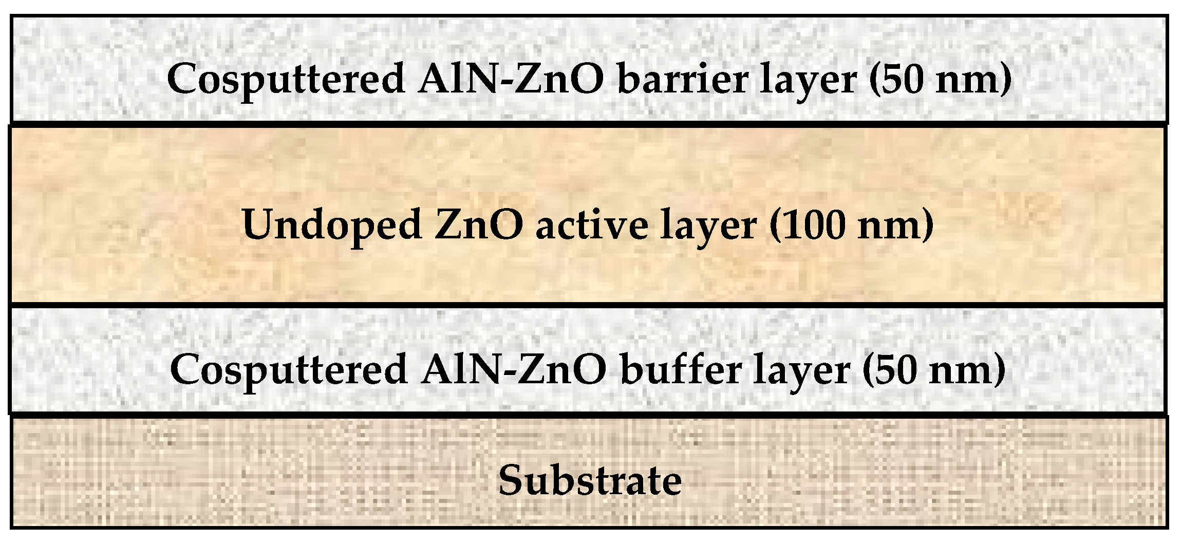
23]. After determining the electrical, optical, and material properties of these annealed undoped ZnO and cosputtered AlN-ZnO films, the crystallinity and radiative properties of a 100-nm thick undoped ZnO film consecutively deposited onto the cosputtered AlN-ZnO film at a thickness of 50 nm using the RF magnetron cosputtering system were investigated, as well as the annealed treatment afterwards. The material and optical properties of the undoped ZnO film sandwiched in between the cosputtered AlN-ZnO films (the AlN-ZnO/ZnO/AlN-ZnO double heterojunction structure is depicted in
Figure 1) that was deposited consecutively by the RF magnetron cosputtering system and then annealed at 700 °C under vacuum ambient for 30 min was also studied.
Film thickness was measured using a surface profile system (Dektak 6M, Veeco, Plainview, NY, USA). The electrical properties of the undoped ZnO and cosputtered AlN-ZnO films as well as the AlN-ZnO/ZnO heterojunction and AlN-ZnO/ZnO/AlN-ZnO double heterojunction structures were investigated using the van der Pauw Hall measurements (Ecopia HMS-5000, Ecopia, Anyang, South Korea) at room temperature. The optical transmittance of the undoped ZnO and cosputtered AlN-ZnO films were examined by an UV-Vis-NIR spectrophotometer (UVD 3500, Labomed, Inc., Los Angeles, CA, USA). Surface morphologies of the undoped ZnO and cosputtered AlN-ZnO films were observed using a field emission scanning electron microscope (FE-SEM, JSM-6700F, JEOL, Akishima, Japan). Radiative characteristics of the single undoped ZnO and cosputtered AlN-ZnO films as well as the heterojunction and double heterojunction structures were investigated from their photoluminescence (PL) spectra measured at room temperature using a home-setup He–Cd laser (λ = 325 nm) as the pumping source. The crystallinity of these samples was determined from X-ray diffraction (XRD) patterns using a diffractometer (Siemens D-500, Siemens, Munich, Germany) with a Cu Kα radiation source. Elemental distributions of the AlN-ZnO/ZnO/AlN-ZnO double heterojunction structures were examined by Auger electron spectroscopy (AES) depth profiles on a scanning Auger nanoprobe (PHI 700, Ulvac-PHI, Kanagawa, Japan). In addition, the Al content in these AlN-ZnO films at the theoretical values of 20% and 40% also had been measured by the energy-dispersive X-ray spectroscope (EDS) quantitative analysis EDS equipment attached to the FE-SEM system (~9.5% and 45.0%) and the AES (~22.1% and 46.7%), respectively.
3. Results and Discussions
Figure 2a shows the optical transmittance of the 300-nm thick undoped ZnO film and cosputtered AlN–ZnO films at theoretical Al atomic ratios of 20% and 40%, respectively, annealed at 700 °C for 30 min under vacuum ambient. All these annealed films exhibited a high optical transmittance at visible wavelengths. The average transmittance at visible wavelengths (400 to 700 nm) of the cosputtered AlN-ZnO (40%) film (~94.5%) was a little higher than that of the undoped ZnO and AlN-ZnO (20%) films (of about 89.0% and 89.8%, respectively).
For the cosputtered AlN-ZnO film at an Al theoretical atomic ratio of 20%, the absorption edge that occurred at the sharp reduction in optical transmittance was found to shift toward a shorter wavelength as compared to the undoped ZnO film, and an apparently blue shift on the absorption edge was observed from the cosputtered AlN-ZnO film as the Al atomic ratio reached 40%. The corresponding optical energy bandgap evaluated from the relationship between (αhν)
2 and photon energy (
Eg) [
25], as shown in the inset figure of
Figure 2b, was markedly widened from 3.26 to 3.87 eV as the AlN was introduced into the ZnO film at a theoretical Al atomic ratio of 40%. As referred to the reports on the energy bandgap of MgZnO and CdZnO alloys modified by the bandgap of MgO (
Eg ≈ 7.7 eV) and CdO (~2.3 eV) [
18,
19,
21,
22], the large energy bandgap of the AlN (~6.3 eV) was likely responsible for the widening optical energy bandgap of the cosputtered AlN-ZnO films, resulting in the high transmittance at the UV wavelengths. Moreover, the higher transmittance of the cosputtered AlN-ZnO at an atomic ratio of 40% around the visible wavelengths was attributed to the lower refractive index of AlN than ZnO.
Table 1 summarizes the electrical properties of the as-deposited and annealed undoped ZnO films as well as the cosputtered AlN-ZnO films at a theoretical Al atomic ratio of 20% and 40% with the thickness of 100 nm, respectively, determined from Hall effect measurements at room temperature. The as-deposited undoped ZnO film showed an insulated nature with a resistivity, ρ, higher than the instrument limit (>10
5 Ω·cm), while the as-deposited AlN-ZnO (20%) film behaved as an
n-type conduction with the electron carrier concentration,
n, of approximately 6.5 × 10
18 cm
−3. The
n-type conduction of the as-deposited AlN-ZnO (20%) was ascribed to the activation of the Al
3+ ions as donor substitutions for the Zn
2+ lattice sites (i.e., Al
Zn) [
23]. However, for the ZnO film cosputtering with the AlN at an Al atomic ratio of 40%, the resistivity of the as-deposited AlN-ZnO (40%) film became too high to be measured. The undoped ZnO film annealed at 700 °C for 30 min under vacuum ambient resulted in
n-type degenerated conduction, while the cosputtered AlN-ZnO film with an Al atomic ratio of 40% still showed insulated behavior.
The reason responsible for the annealed undoped ZnO film possessed a high electron carrier concentration (~1.7 × 10
19 cm
−3) with a hall mobility, μ
n, of 12.9 cm
2/V·s was attributed to the presence of the native oxygen vacancies (V
O) during the film re-crystallization. In addition, this post-annealing treatment also led to both an increase in carrier concentration (~6.8 × 10
19 cm
−3) and hall mobility (9.0 cm
2/V·s) of the ZnO film cosputtered with AlN at an Al atomic ratio of 20% as compared to that of the as-deposited film, revealing that more Al
Zn donors had been activated, and the crystalline structure was improved. Moreover, since the donor level of the Al
Zn was much closer to the conduction band (~51 ± 4 meV) of the ZnO compared to that of the V
O donor (~566 ± 62 meV), as referred to the report [
24], the Al
Zn donors were prone to be activated at room temperature. Thus, a very high electron concentration was measured from the as-deposited AlN-ZnO film at the Al content of 20%.
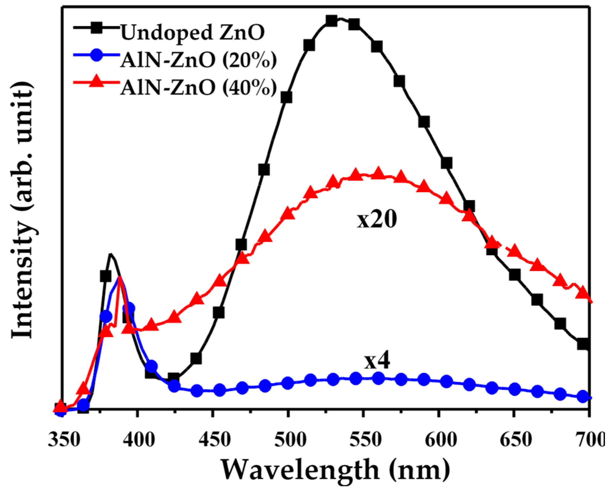
Figure 3 gives the room temperature PL spectra of the 100-nm thick undoped ZnO and cosputtered AlN-ZnO films annealed at 700 °C for 30 min under vacuum ambient. The signal of the cosputtered AlN-ZnO film with Al atomic ratios of 20% and 40% was magnified by 4 and 20 times, respectively, to make the observations more efficient.
The PL spectrum of the annealed undoped ZnO film exhibited a dominant visible wavelength emission and a short-wavelength emission that were in turn assigned as the emissions from the deep-level (DL) and near-band-edge (NBE) transitions, respectively [
26,
27]. As quoted from the reports [
28,
29], the DL emission at about 535 nm is mainly composed of the V
O-related transitions as a consequence of the post-annealing treatment under vacuum ambient being favorable for the outdiffusion of the oxygen atoms in the ZnO film. By contrast, such DL emission was almost absent in the PL spectrum of the AlN-ZnO (20%) cosputtered film, revealing that the V
O-related transitions were effectively suppressed when AlN was introduced into the ZnO film. The reason responsible for the marked decrease in the formation of the oxygen vacancies was ascribed to the substitution of Zn
2+ lattice sites by the Al
3+ ions, which stabilized the oxygen atoms more efficiently due to the bond dissociation energy of Al–O (~511 kJ/mol) being much higher than that of Zn–O (~211 kJ/mol) [
15,
30]. In addition, the activation of Al and N dopants in the ZnO film also led to a red shift of the short-wavelength emission from 382 to 388 nm. When the cosputtered AlN-ZnO film had an Al atomic ratio of 40%, the annealed sample emitted a very weak PL signal that featured a short-wavelength peak at 388 nm and a broad long-wavelength emission extending from near-ultraviolet to near-infrared wavelengths, implying that defects other than V
O were formed in the AlN-ZnO (40%) film.
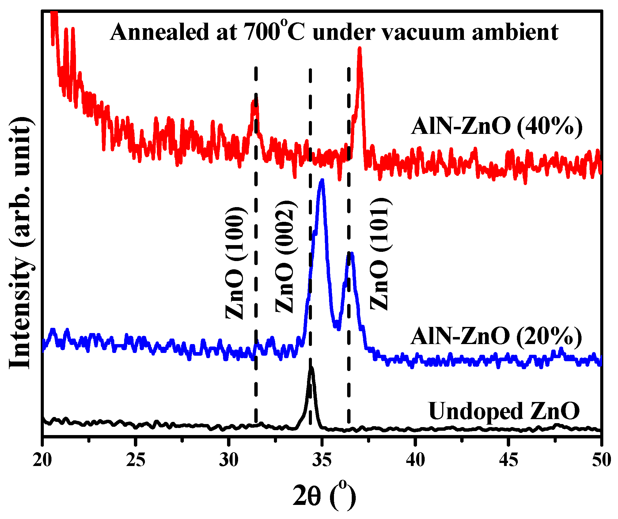
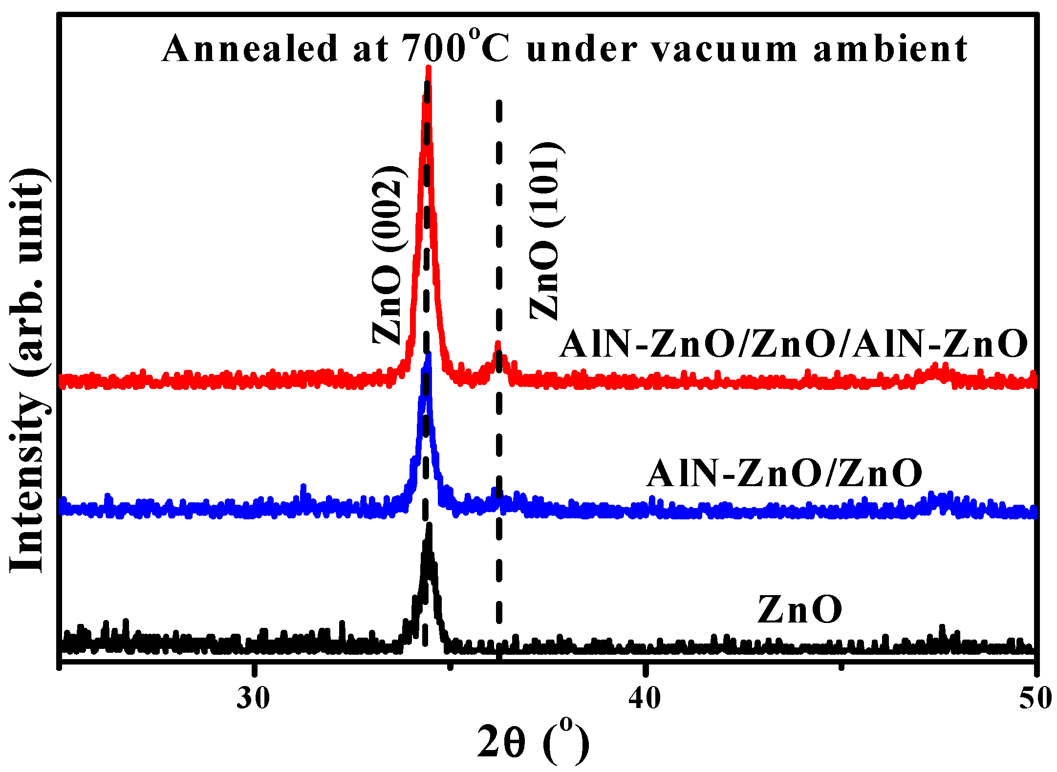
Figure 4 shows the XRD patterns of the 300-nm thick undoped ZnO films and cosputtered AlN-ZnO films with Al atomic ratios of 20% and 40%, respectively, after annealing at 700 °C under vacuum ambient for 30 min.
The XRD pattern of the annealed undoped ZnO film showed only one peak approximately at 34.46° (assigned as ZnO (002) phase according to JCPDS no.36-1451), revealing the preferred growth orientation along the
c-axis. Compared to the undoped ZnO film, the full width at half maximum (FWHM) of the ZnO (002) peak was widened and another peak at about 36.62° (identified as ZnO (101)) was observed from the XRD pattern of the annealed AlN-ZnO (20%) film. This implied that the introduction of the AlN into the ZnO film would break the
c-axis growth orientation. In addition, the shift of the ZnO (002) peak to a high 2θ value (~35.02°) also showed evidence of the activation of Al
3+ ions as donor substitutions for Zn
2+ lattice sites, since the ionic radius of the Al atom (0.053 nm) was smaller than that of the Zn atom (0.072 nm). When the theoretical Al atomic ratio in the AlN-ZnO film further increased to 40%, the structure further degraded to an amorphous-like structure, since the ZnO (002) phase was hardly observed, and only weak ZnO (100) and (101) phases were observed in the XRD pattern. Incorporating into the electrical property of these cosputtered AlN-ZnO films, although the activation of the Al
3+ donors in the ZnO matrix was favorable for the enhancement on the electron carriers, the introduced AlN would also break the structure order of the ZnO film as resulted from the decrease in the
c-axis growth orientation. Accordingly, the amorphous-like AlN-ZnO film—which implied the undue disorder of the ZnO structure—exhibited the insulated nature with a very high resistivity (>10
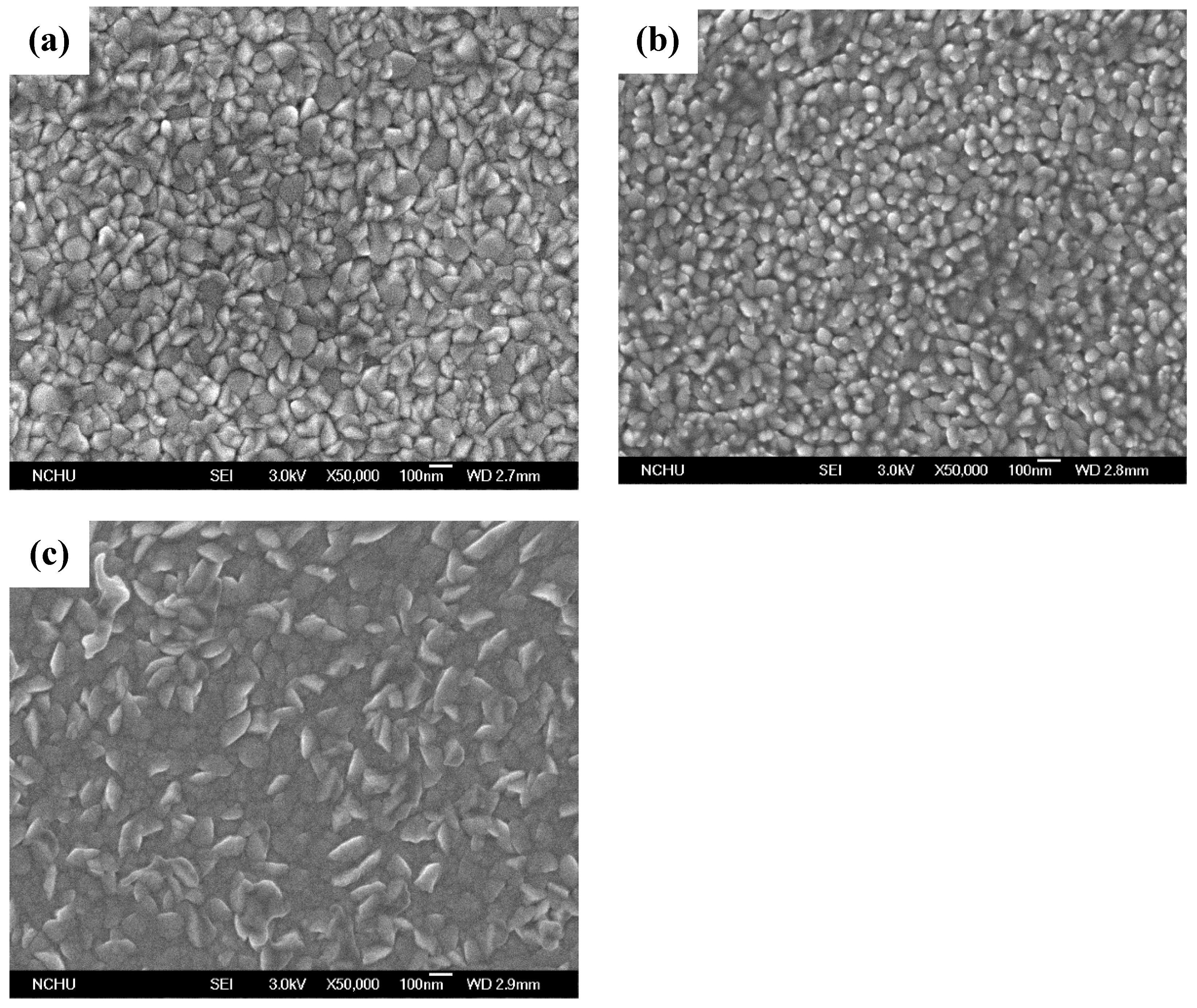
5·Ω cm). The surface morphologies of these annealed films observed from the FE-SEM measurements are given in
Figure 5a–c. In
Figure 5a, irregular wedge-like grains were clearly seen on the surface of the annealed undoped ZnO film.
These textured grains distributed over the surface of the AlN-ZnO (20%) cosputtered film (
Figure 5b) became small and round-like, which also confirmed an inferior crystalline structure compared to the undoped ZnO film shown in
Figure 4. Furthermore, the amorphous-like structure obtained from the ZnO film cosputtered with the AlN at a theoretical Al atomic ratio of 40% provided an ambiguous surface morphology with sheet-like protrusions, as observed from
Figure 5c.
Based on the investigations of the annealed cosputtered AlN-ZnO films, the introduction of AlN into the ZnO film resulted in a widening of the optical energy, and was also beneficial for suppressing the formation of native oxygen vacancies. The undoped ZnO film sandwiched in the cosputtered AlN-ZnO films with high optical energy bandgap was then designed for the purpose of confining the carriers in the undoped ZnO film. The electrical properties of the undoped ZnO film deposited onto the substrate with and without an AlN-ZnO (20%) buffer layer, as well as the ZnO film sandwiched in the cosputtered AlN-ZnO films, after annealing at 700 °C under vacuum ambient for 30 min are summarized in
Table 2. The resistivity of the ZnO film deposited onto an AlN-ZnO buffer layer and the AlN-ZnO/ZnO/AlN-ZnO double heterojunction structure were both lower than the ZnO film directly deposited onto the silicon substrate. The main reason for the improvement in the structure resistance seemed to be different when considering their different impacts on carrier concentration and mobility. For the undoped ZnO film deposited onto the AlN-ZnO buffer layer, the slight improvement in structure resistivity (~2.68 × 10
−2 Ω·cm) as compared to the ZnO film directly deposited on the substrate (~2.89 × 10
−2 Ω·cm) was attributed to an almost double increase in carrier mobility (from 12.9 to 24.4 cm
2/V·s), even with a decrease in structure carrier concentration (~9.6 × 10
18 cm
−3). This implied that the ZnO film deposited onto the AlN-ZnO buffer layer was beneficial for reducing the mechanisms of the impurity and/or lattice scatterings for carriers transport in the ZnO film. In contrast, for a cosputtered AlN-ZnO barrier layer coated onto the AlN-ZnO/ZnO structure, there was a marked reduction in structure resistivity of about 7.02 × 10
−3 Ω·cm, which was mainly attributed to an obvious increase in the carrier concentration (~4.6 × 10
19 cm
−3). This revealed that indiffusion of the Al
3+ ions as donor substitutions for the Zn
2+ lattice sites in the undoped ZnO film resulted in an increase in the electron carriers, which became the main mechanism responsible for the reduction in the structure resistivity. The crystalline structures investigated from XRD measurements for these annealed samples are shown in
Figure 6.
All of these samples show a preferred
c-axis ZnO (002) growth orientation. Compared with the diffraction pattern of undoped ZnO film directly deposited onto the substrate, film deposited onto an AlN-ZnO buffer layer resulted in an intense ZnO (002) signal with a peak position (~34.44°) closer to that which appeared in the bulk ZnO film (~34.43°), revealing that the internal stress residing in the undoped ZnO film was further optimized [
26]. By adapting the Debye–Scherer formula, crystal size,
D, is obtainable from of the FWHM of the preferred orientation (ZnO (002)) [
31]:
where k is a constant; λ is the wavelength of the X-ray radiation; and β and θ are the FWHM in radians and the diffraction peak position of the ZnO (002) phase, respectively. The crystal size of the undoped ZnO film deposited onto an AlN-ZnO buffer layer, as listed in
Table 2, increased from about 23 to 29 nm. The growth of the crystal size for the undoped ZnO film deposited onto the AlN-ZnO buffer layer, which corresponded to fewer grain boundaries, was beneficial for lowering the possibility of carrier scattering, and thereby resulted in the apparent increase in carrier mobility shown in
Table 2.
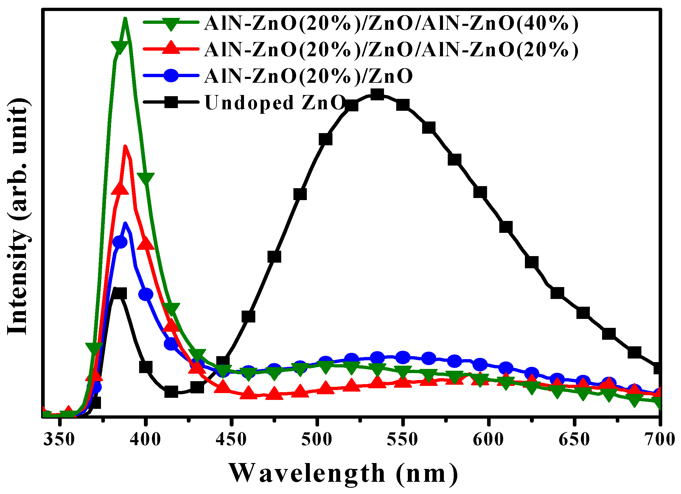
When AlN-ZnO was coated onto the AlN-ZnO/ZnO structure, the ZnO (002) signal was more intense than that in the spectrum of the AlN-ZnO/ZnO structure, while the peak position and FWHM of the ZnO (002) phase were almost identical to that of the AlN-ZnO/ZnO structure. In addition, another weak diffraction peak associated with the ZnO (101) phase mainly emerged from the top AlN-ZnO layer, which was also observed in the XRD spectrum. The room temperature PL spectra of the undoped ZnO film deposited onto the substrate with and without an AlN-ZnO (20%) buffer layer are shown in
Figure 7.
Compared to the undoped ZnO film directly deposited onto the substrate, the visible wavelength luminescence associated with the DL transitions in the ZnO film almost was absent in the PL spectrum of the undoped ZnO film deposited onto the AlN-ZnO buffer layer, and thereby only one peak was measured around the ultraviolet wavelength. Thus, the native defects in the ZnO film associated with the oxygen vacancies were effectively suppressed as it was deposited onto the cosputtered AlN-ZnO film. Furthermore, although an intense and single UV emission was achievable from the AlN-ZnO/ZnO structure, this peak red-shifted from 382 toward 388 nm with a widened FWHM of 30 nm as compared to the single ZnO film (~20 nm).
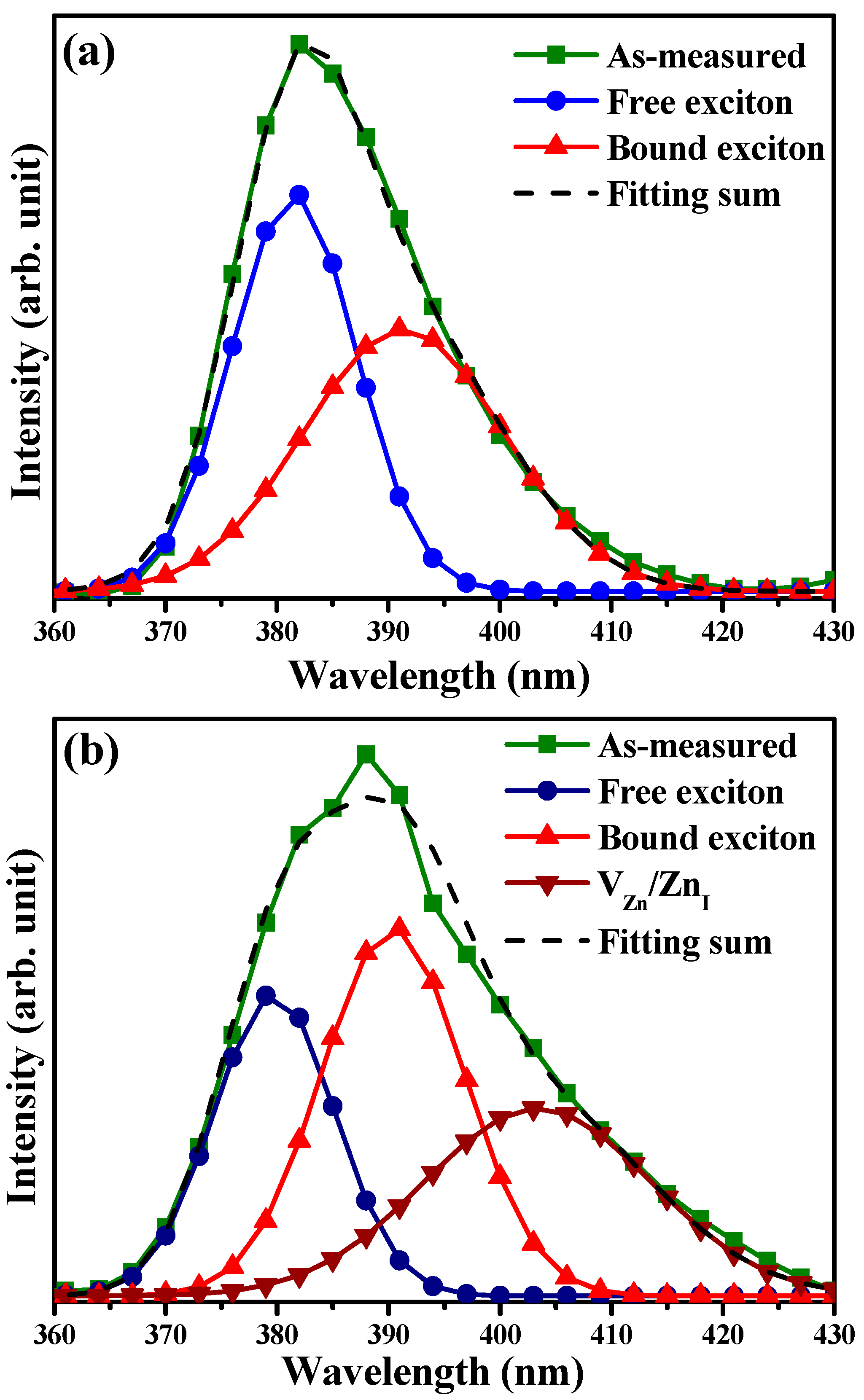
Figure 8a,b give a deconvolution on this UV light luminescence that emerged from the single ZnO film and AlN-ZnO/ZnO structure, respectively, to extract the reason for the changes of peak position and the wide FWHM of this short-wavelength emission. As quoted from previous reports [
32,
33,
34], the short-wavelength luminescence emitted from the undoped ZnO film directly deposited onto the substrate (
Figure 8a) was deconvoluted into two curves with peaks at 382 and 391 nm, which were in turn characterized as the recombination of the free exciton and bound exciton associated with the donor and/or acceptor impurities, respectively.
In contrast to the single ZnO film, the relative intensity of the bound exciton emission became higher than that of the free exciton emission as deconvoluted from the short-wavelength luminescence of the ZnO film deposited onto the cosputtered AlN-ZnO film (
Figure 8b), thereby leading to the red-shift of the UV light luminescence. In addition, another weak peak at about 403 nm deconvoluted in
Figure 8b was likely responsible for widening FWHM of the short-wavelength emission. According to the reports [
24,
35], the transitions of zinc vacancy (V
Zn)/zinc interstitial (Zn
I) in the ZnO film was responsible for this radiative emission. Although the above-mentioned studies showed that single UV photoluminescence was achievable from the AlN-ZnO/ZnO heterojunction structure due to the suppression of native defects related to oxygen vacancies in the undoped ZnO film, luminescence intensity was limited due to defects distributed over the ZnO surface and the low recombination efficiency of the photogenerated electron–hole pairs (ehps) in the active ZnO film. With the aims to passivate the surface states of the ZnO film and also restrict the radiative recombination of the photogenerated ehps within the ZnO active layer, a cosputtered AlN-ZnO film with a wider optical energy bandgap was designed to consecutively deposit onto the undoped ZnO film. The PL spectra of the AlN-ZnO/ZnO heterojunction structure coated by a cosputtered AlN-ZnO film at the Al atomic ratios of 20% and 40%, respectively are given in
Figure 7. The enhancement of the UV light luminescence for the AlN-ZnO/ZnO structure coated by the cosputtered AlN-ZnO film at an atomic ratio of 20% as a result of the improved confinement of the photogenerated ehps in the ZnO active layer was significant. The structure coated by the cosputtered AlN-ZnO film at an atomic ratio of 40% had a wide optical energy bandgap of 3.58 eV, and the resulting UV light luminescence could be further optimized to a factor that was about two times higher than that of the luminescence from the AlN-ZnO/ZnO heterojunction structure.
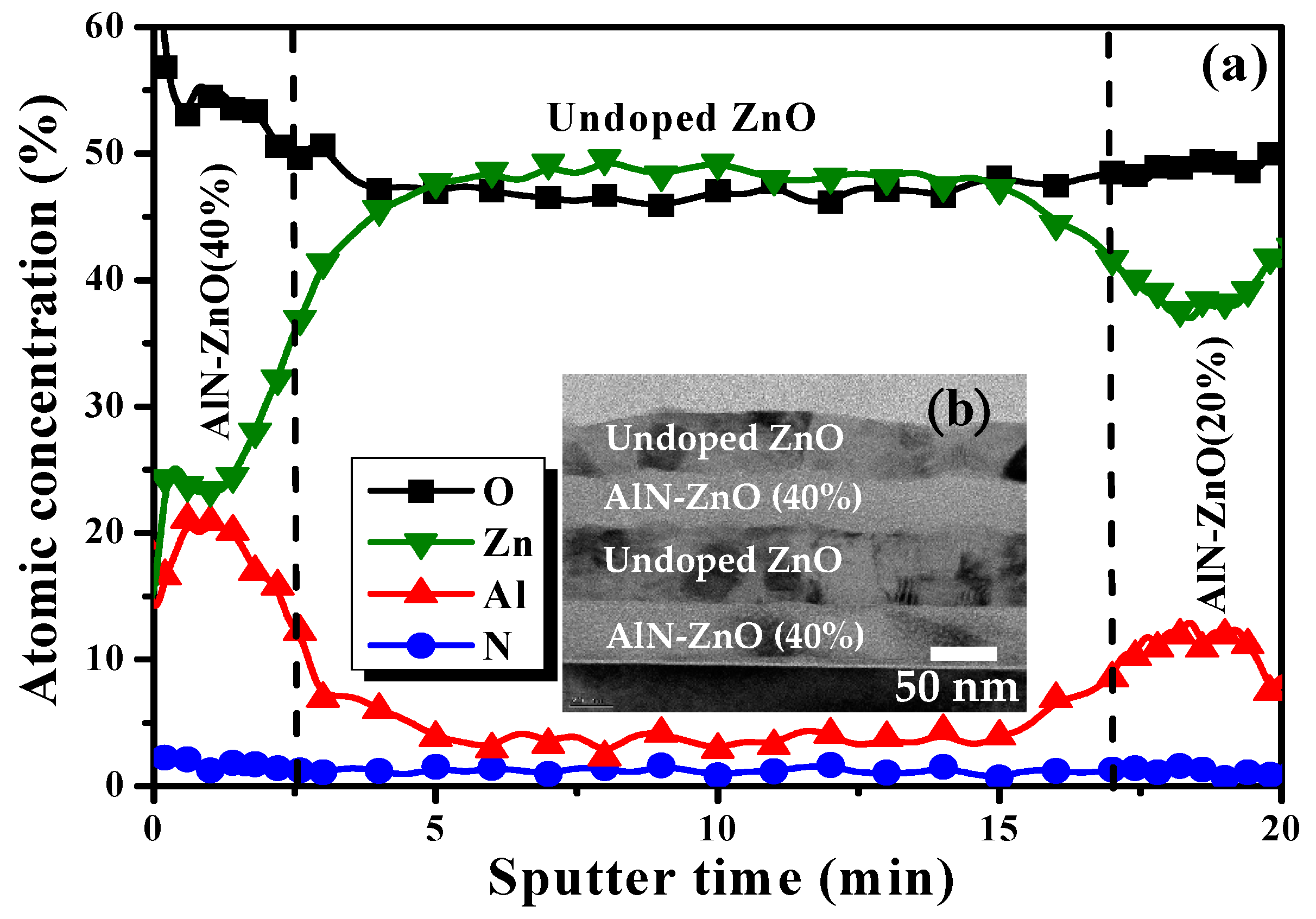
Figure 9a shows the elemental depth profiles of the Al, N, Zn, and O atoms for the AlN-ZnO (20%)/ZnO/AlN-ZnO (40%) double heterojunction structure from AES measurement (the inset figure (
Figure 9b) shows the symmetric AlN-ZnO (40%)/ZnO/AlN-ZnO (40%) DH structure with the thickness of about 35 nm/50 nm/35 nm conducted from the cross-sectional TEM observations).
Layers of the cosputtered AlN-ZnO and undoped ZnO films can be identified through the evolution of these elements. At the bulk of the undoped ZnO region, the elemental concentration of the O atoms was a little lower than that of the Zn atoms, whereas the atomic concentration of the O element was gradually increased around the AlN-ZnO/ZnO interface. At the cosputtered AlN-ZnO region, the Al element distributed over the top layer almost was higher by double over that of the Al atoms at the underlayer, while the atomic concentration of the N element at the cosputtered AlN-ZnO films was limited to a low value of about 1.5 at.% to 2 at.%, revealing the insolubility of nitrogen atoms into the cosputtered AlN-ZnO film, as described previously [
23]. In addition, the indiffusion of Al atoms into the undoped ZnO film was evident, as an extending tail was observed around the AlN-ZnO/ZnO interface. The indiffusion of the Al atoms resulted in an increase of O atoms at the AlN-ZnO/ZnO interface further confirmed the mechanism responsible for the improvement in the structure resistivity owing to the activation of the Al
Zn donors and suppression of the V
O defects in the undoped ZnO film.


