Abstract
Ultra low power circuits require robust and reliable operation despite the unavoidable use of low currents and the weak inversion transistor operation region. For analogue domain filtering doubly terminated LC ladder based filter topologies are thus highly desirable as they have very low sensitivities to component values: non-exact component values have a minimal effect on the realised transfer function. However, not all transfer functions are suitable for implementation via a LC ladder prototype, and even when the transfer function is suitable the synthesis procedure is not trivial. The modern circuit designer can thus benefit from an updated treatment of this synthesis procedure. This paper presents a methodology for the design of doubly terminated LC ladder structures making use of the symbolic maths engines in programs such as Matlab and Maple. The methodology is explained through the detailed synthesis of an example 7th order bandpass filter transfer function for use in electroencephalogram (EEG) analysis.
1. Introduction
Despite the rise of digital filters, analogue domain filters are still an essential part of many electronic systems; for example in high frequency circuits where high frequency and high resolution ADCs are ostly [1]. Increasingly analogue filters are also being used in low frequency applications such as in analogue signal processing units in wearable physiological sensors; see [2–4] as examples. For such battery powered physiological monitors power efficiency is essential, and the use of analogue signal processing allows the low dynamic ranges and signal-to-noise ratios of many biological signals to be exploited. It is well known that analogue filters are potentially much more power efficient than their digital counterparts in such circumstances [5,6].
At the circuit level, many different analogue filter topologies are available, with cascades of second order sections [7] and orthonormal ladder filters [8] being popular choices for on-chip implementation. However, at both very high and very low frequencies parasitic components become significant in the circuit design of the filter. Also, for low power and low voltage circuits the use of transistors operating in the weak inversion region is unavoidable (due to the intrinsically low drain currents provided), although this comes at the cost of decreased transistor current matching. For robust analogue filters in these situations it is essential that the sensitivity of the filter transfer function to non-exact component values is minimised: device mismatch and parasitic components should not change the shape of the implemented frequency response.
Filters based upon LC ladder prototypes, where the filter transfer function is implemented by lossless inductor and capacitor elements connected between terminating resistances (see Figure 1), are known to have very low sensitivities to non-exact component values [9]. Indeed [9] notes that doubly terminated LC ladders with equal terminating resistances are “very nearly an optimum realization for filter functions”.
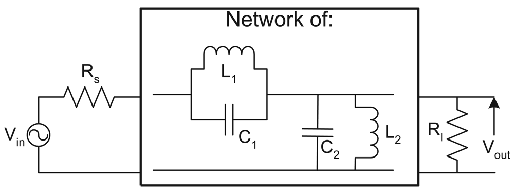
Figure 1.
A generalised doubly terminated LC ladder filter. Doubly terminated LC ladder filters consist of inductors (L) and capacitors (C) connected in series and in shunt between a source resistance (Rs) and a load resistance (Rl). Doubly terminated networks with equal terminating resistances have the lowest sensitivity to non-exact component values. Singly terminated networks have only one of the terminating resistances present and act as a starting point for the synthesis of a doubly terminated network.
Unfortunately, not all transfer functions can be implemented as doubly terminated LC ladder topologies. Even when these topologies are possible, the synthesis procedure—moving from the wanted s domain transfer function to a suitable ladder structure and component values—is not straight-forward. This is particularly true when the filter response is not one of the standard filter approximations (Butterworth, Chebyshev, Bessel and similar). Whilst fundamental ladder synthesis procedures were established in the early twentieth century [10] and a number of reference texts and software tools exist (for example [9,11–16]) the modern circuit designer can benefit from an updated treatment of the subject, particularly for cases where automated design software does not give a satisfactory solution, or a solution t all. For example, ladder optimisation techniques have recently been proposed [17,18], but can only be used once a suitable starting network is available.
This paper re-visits and reviews the synthesis procedure for the generation of doubly terminated LC ladders. In particular we focus on the use of symbolic maths engines in programs such as Matlab and Maple and their ability to solve non-linear simultaneous equations. For the review this allows more insight into the synthesis procedure as opposed to using Matlab to automate the insertion loss method of classical LC synthesis [19], or implementing known recursion formulae for the standard filter approximations [16]. The procedure considered here can handle non-standard filter approximation transfer functions.
Inevitably it is not possible to consider all possible design cases and issues in one article; instead a refreshed overview of the topic is provided. To keep the description here clear and concise the main body of the paper presents the detailed design of a non-trivial, high order, real-life LC ladder filter transfer function. The example used here takes the previously reported transfer function from [20]:
and finds a doubly terminated LC ladder filter that implements the transfer function. This particular function is chosen for the example case as it is one for which popular synthesis programs [21,22] are not capable of finding a doubly terminated LC ladder topology for, although one is possible. The transfer function itself is of interest as it corresponds to a 7th order bandpass filter with a centre frequency of 2.1 Hz and has been used in [23] for the automated processing of electroencephalogram (EEG) signals in portable recorders. For completeness we also briefly present the procedure for moving from the synthesised LC ladder prototype to a gmC topology that simulates the found LC ladder and that is suitable for on-chip implementation. In addition, a detailed summary of the method used is provided to aid in the design of other transfer function cases.
The remainder of this paper is structured as follows. Section 2 presents some prerequisites of circuit theory necessary for the synthesis procedure. This is to ensure that there is no confusion in terminology used in future sections. Section 3 then presents a design procedure for a singly terminated LC ladder network as the starting point to obtain a doubly terminated network. The generation of a doubly terminated topology is then given in Section 4. The derivation of both of the singly and doubly terminated topologies are given for the minimum capacitor case, and the minimum inductor counterpart is considered in Section 5. The topologies are also derived assuming terminating resistors of 1 Ω. Section 6 presents the component scaling to give values that are more realistic for on-chip implementation and Section 7 presents the gyrator substitution for the inductors which cannot be implemented on-chip. This gives an end gmC filter suitable for on-chip implementation. Finally, a summary of the methods used in this paper is given in Section 8.
2. Prerequisites
An amount of terminology is essential for the LC ladder synthesis procedure. This will already be familiar to most readers, in which case it may be skipped, but nevertheless the needed terminology is re-defined here to ensure that only consistent and clear terminology is used in the remainder of the paper.
2.1. Even and Odd Functions
An even function is one that satisfies the condition
In general an even polynomial is of the form
where 2i will always be an even number. In contrast an odd function satisfies the condition
and odd polynomials are of the form
where 2i + 1 will always be an odd number.
Given a polynomial f(x) it is thus possible to separate it into a sum of odd and even parts by separating the odd and even powers of x.
2.2. Hurwitz Polynomials
A Hurwitz polynomial is one that has all of its poles in the open left hand plane of the s = σ + jω axis. That is, poles can occur in positions for which σ = 0 or σ < 0. A strictly Hurwitz polynomial is one for which all of the poles are in the closed left hand plane, those with σ < 0.
2.3. Transmission Zeros
Given a transfer function T(s) the transmission zeros are the values of s for which T(s) = 0. If T(s) is of the form
transmission zeros occur at the zeros of T(s) that is the roots of N(s). Also, if the order of D(s) is greater than N(s), T(s) → 0 as s → ∞ and so transmission zeros are also present at s → ∞.
2.4. y Parameters
y parameters (short circuit admittance parameters) provide a method for describing a two port network purely by functions of the input and output. The overall behaviour is described as
and the y parameters can be derived as
For a passive network y12 = y21. It is also possible to define z parameters (open circuit impedance parameters) to describe a network as
where
In general a yij or zij is known as an immittance parameter and the procedure for generating a LC ladder is to derive the required forms of the immittance parameters from the wanted transfer function and then to find LC ladder topologies that realise these functions.
For a given circuit it is possible to find the y parameters by writing down the nodal analysis matrix: diagonal elements are given by the sum of the admittances attached to a node and off-diagonal elements aij are always negative and given by the admittance between nodes i and j. The
pivotoperation in Maple can then be used to perform Gaussian elimination and reduce the nodal analysis matrix to a 2 × 2 form, giving the y parameters. An example of this is given in Section 3.3.
2.5. Private Poles
In general all four y parameters are functions of the same circuit and so have the same poles. However, it is possible for poles to be present in y11 and y22 that are not present in y12. These correspond to elements at the ports of the network such that when y12, for example, is found with V1 = 0 they have no effect on the circuit being analysed and so do not appear in y12. For example, when V1 = 0 for the determination of y12, any shunt component at port 1 will be shorted and so cannot affect the circuit operation. When, and in general, V1 ≠ 0 the shunt components will affect the nodal equations and so they do appear in y11. Poles which are present in y11 and/or y22 but not y12 are known as private poles.
2.6. Realisability Criteria
The core constraints on an arbitrary transfer function to be realisable as an LC ladder structure are that its numerator must be a purely even or odd function of s and that its denominator must be a strictly Hurwitz polynomial. This latter condition is somewhat obvious in the fact that it corresponds to the transfer function being stable in the open loop.
3. Singly Terminated LC Ladder Synthesis
3.1. y Parameter Generation
Based upon classical synthesis procedures [9,12,13] the starting point for the generation of a doubly terminated LC ladder network is the generation of a suitable singly terminated network as illustrated in Figure 2. For both cases in Figure 2 the input is Vin(s) and in case (a) the output is a voltage, while in case (b) the output is a current, but otherwise the two set-ups are identical. Considering case (b) (case (a) is similar but in terms of the z parameters) the input voltage to output transfer function is given by
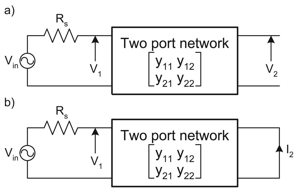
Figure 2.
Two singly terminated two port networks with the output (a) as a voltage and (b) as a current.
For simplicity a design is considered for the case Rs= 1 Ω. From this prototype the end component values can then be scaled to match the wanted terminating resistor, see Section 6. The obtained A(s) is thus of the form
In comparison, the wanted transfer function, (2), is of the form
where N(s) is an even function and D(s) is a strictly Hurwitz polynomial. Separating D(s) into its odd (Do(s)) and even (De(s)) parts
From this, analytic forms for the required y parameters can easily be found. If the wanted transfer function is
where
the required y12 and y11 are then
where
| a | = | 6.88 × 10⁻³ |
| b | = | 2.34 × 10⁻⁸ |
| c | = | 1.34 × 10⁻⁶ |
| d | = | 3.70 × 10⁻⁵ |
| e | = | 6.79 × 10⁻⁴ |
| f | = | 8.67 × 10⁻³ |
| g | = | 0.075 |
| h | = | 0.4 |
| a′ | = | a/h |
| = | 1.72 × 10⁻² | |
| b′ | = | b/h |
| = | 5.85 × 10⁻⁶ | |
| d′ | = | d/h |
| = | 9.25 × 10⁻⁵ | |
| f′ | = | f/h |
| = | 2.17 × 10⁻² |
From (18), for a singly terminated network the form of y22 is not significant.
3.2. Transmission Zero Realisation
The design procedure now proceeds by examining the form of y11 and y12. y11 has a private pole (one that is not present in y12), given by hs. This results in a transmission zero at s = 0. y12 has six transmission zeros: one at s = 0 due to the numerator a′s; and five at s → ∞ due to the difference in order between the numerator and denominator.
The key to LC ladder synthesis is realising the correct positions of all of these zeros using suitable arrangements of components and then choosing the values of the components so that y11 is numerically satisfied. The realised y12 can then differ by at most a constant gain factor from the wanted y12, which corresponds to the LC ladder matching the wanted filter shape, but not necessarily the gain. However, this can be readily compensated for by the presence of an ideal transformer, amplifier, or simply compensating for the expected values in the next part of any end system.
A transmission zero at the origin can be realised by one of the arrangements in Figure 3a—a series capacitor or a shunt inductor. A transmission zero at infinity corresponds to one of the elements in Figure 3b—a series inductor or a shunt capacitor. For completeness, although it is not required in the example here, it is possible to realise zeros at arbitrary frequencies through the use of one of the elements in Figure 3c which realise a zero at ω = (LC)−1/2. Also, it is possible to shift the position of zeros through the use of a partial pole removals [12], but this is not explored further here.
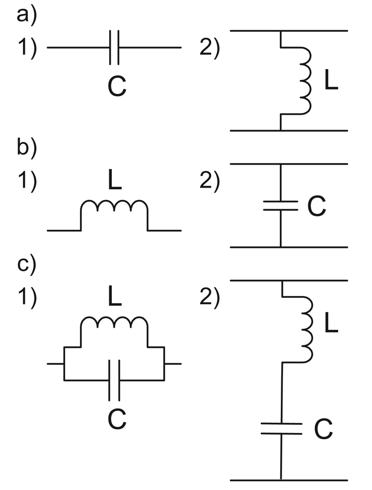
Figure 3.
Realising transmission zeros. (a) Two alternative elements that realise a transmission zero at s= 0; (b) Two alternative elements that realise a transmission zero at s → ∞; (c) Two alternative elements that realise a transmission zero at ω = (LC)−1/2.
To realise the network it is simply a matter of arranging the potential elements from Figure 3 so that all of the transmission zeros are provided and the combinations of elements do not cancel out. For example, in principle two transmission zeros at s = 0 could be realised by a cascade of capacitors as illustrated in Figure 4. In practice of course this is not possible, the two capacitors in series are equivalent to just one capacitor of a different value and so only one transmission zero is realised.
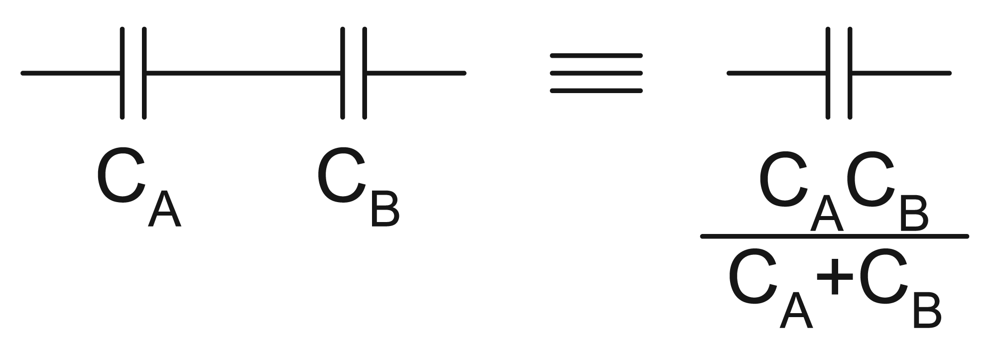
Figure 4.
In principle two cascaded capacitors realise two transmission zeros but do not in practice.
Ideally combinations of the networks illustrated in Figure 5 are used to order the elements to give the required poles. These networks correspond to Foster 1, Foster 2, Cauer 1 and Cauer 2 realisations and are used as the resulting component values can be readily found by simple manipulations of the wanted immittance function. For a Foster 1 realisation the component values are given by the partial fraction expansion
while for the Foster 2 form the values are given by the alternative partial fraction expansion
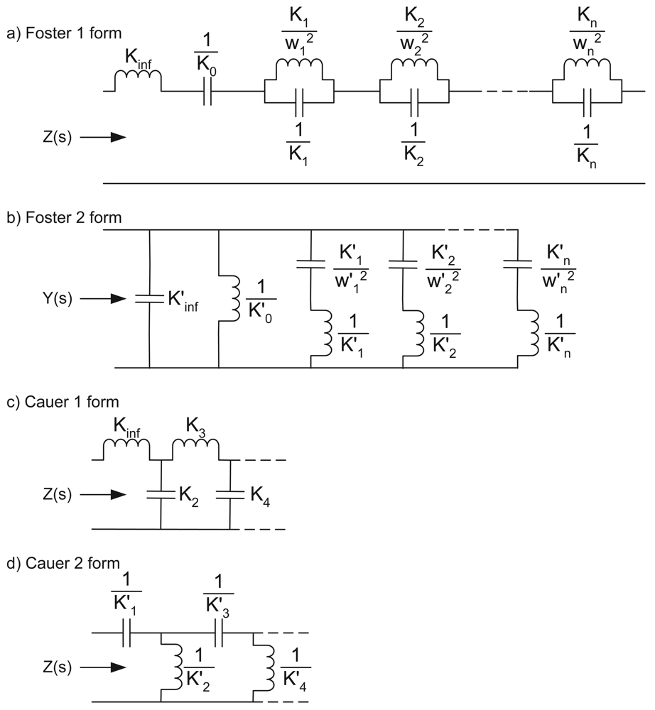
Figure 5.
Foster and Cauer network realisations. These allow simple determination of the required component values by continued and partial fraction expansions.
For the Cauer 1 realisation the component values are given by a continued fraction expansion around infinity
and the Cauer 2 values are given by a continued fraction expansion around zero
Unfortunately, due to the arrangements of zeros needed a Cauer based network does not give a satisfactory result (see Section 3.4). We utalise an alternative method based upon the solution of non-linear simultaneous equations to provide the wanted network.
3.3. Network Synthesis
It is clearly seen that the network to be synthesised needs two elements from Figure 3a to realise the transmission zeros at the origin and five elements from Figure 3b for the transmission zeros at infinity. Furthermore one of the zeros at the origin must be private to y11 and so must be realised at port one of the network, not in the middle. A network that satisfies these requirements without any elements cancelling is given in Figure 6. This has the nodal matrix (31) and the y parameters (32), (33).

Figure 6.
A prototype network with the desired y parameters for a singly terminated ladder.
From these it can be seen that y11 and y12 are indeed of the correct form (have the same structure in terms of the number of poles and zeros). It is noted that due to the series connection of an inductor and capacitor to port two of the network, for the derived y parameters to be valid it is necessary to draw a current through this branch of the circuit. The transfer function implemented thus has to be of the form in Figure 2b.
From (32) and (33), and introducing βL3 = L4 to allow the equations to be written in a more compact form, the coefficients of the implemented y parameters can be extracted as
Comparing the coefficients of (25), (26), to (34)–(41) a series of multiplicative simultaneous equations are thus formed. To find the required component values it is simply a matter of solving this set of equations:
Note that there are only seven component parameters, but eight equations. An exact solution is thus not possible. In general, the first equation, (42), corresponds only to the passband gain of the filter. By ignoring this equation, it is possible to solve for the other equations. Again, this gives the wanted filter shape and the passband gain can be corrected for elsewhere as discussed previously.
The multiplicative simultaneous equations are readily solved using the Maple or Matlab
fsolvetool for the solution of non-linear simultaneous equations. Based on convergence issues however, (and due to the potential presence of local and global solutions) an initial guess at the component values needs to be provided. Based upon this different solutions may be found and it is not guaranteed that all the component values will be found exactly, or will be positive.
If a starting guess that gives only positive component values cannot be found it is possible instead to view the solution of the equations as a constrained minimisation problem which can be solved via the
where x represents each simultaneous equation (b–h) and each equation is a function of the component values
fminconfunction. In brief, the equations to be solved, (42)–(49), are rearranged into a cost function. Typically this is of the form of a sum of the square of the residuals:
Alternative cost functions, such as using l1 and Huber norms, rather than the l2 norm, are also possible and could be used if desired, as could any desired optimisation technique. Ideally F(x) = 0, and it cannot be negative, so the optimisation problem is now simply a matter of minimising F(x) subject to the constraint that 0 < x < ∞ for all of the arguments of x.
Solving these equations for the singly terminated LC ladder gives the required component values. The best approximation found is given by
which gives a network with a centre frequency gain 1.4 times the wanted gain, which would need to be compensated for elsewhere. The full form of the singly terminated LC ladder filter is thus shown in Figure 7 where it is noted that the input signal is voltage mode while the output signal is current mode. The resulting Bode magnitude response is shown in Figure 8. The 1.4 gain factor between the wanted and implemented responses is clearly seen, as is the correct response shape.
| C1 | = | 24.1 mF |
| C2 | = | 60.6 mF |
| C3 | = | 48.6 mF |
| L1 | = | 364.5 mH |
| L2 | = | 123.4 mH |
| L3 | = | 18.3 mH |
| L4 | = | 400 mH |

Figure 7.
The final singly terminated LC ladder filter with component values.
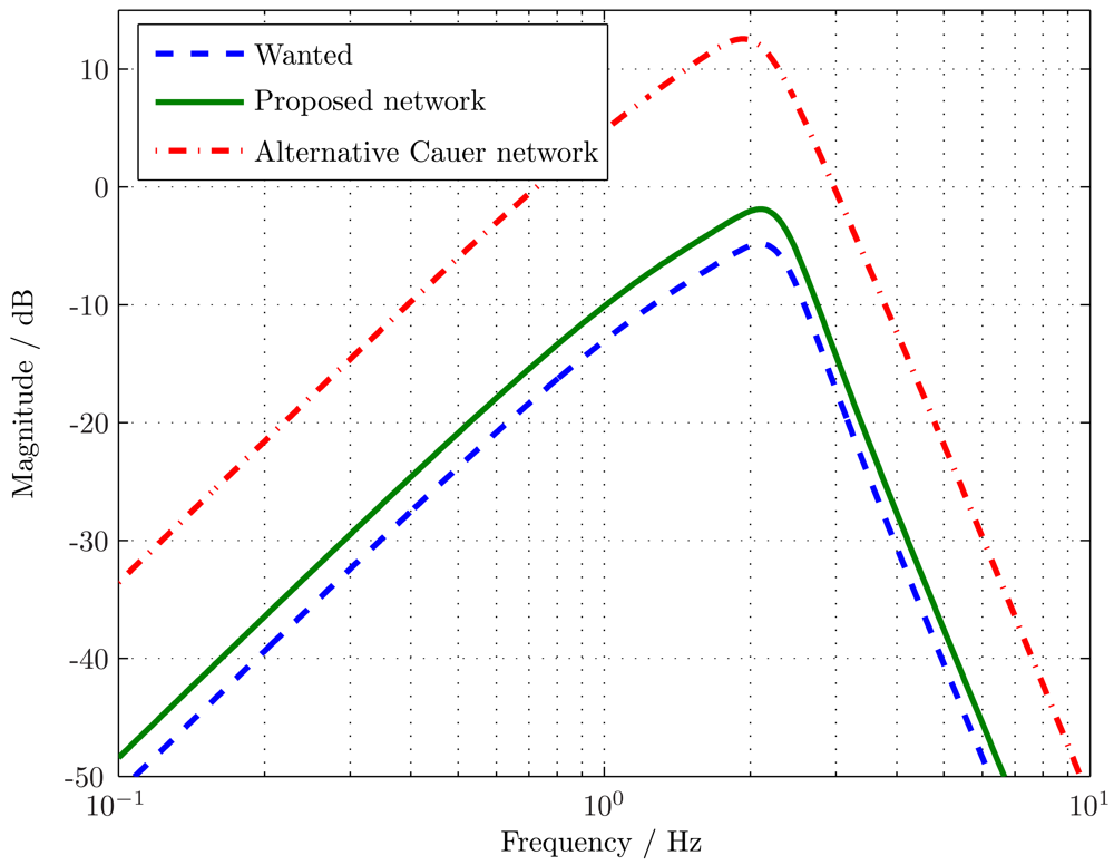
Figure 8.
Bode magnitude responses for the singly terminated LC ladder networks. The proposed network (Figure 7) matches the wanted response well, given an arbitrary gain difference of 1.4. In contrast the network based upon cascades of Cauer networks (Figure 9) shows a deviation from the wanted response at frequencies just below the centre frequency.
3.4. Alternative Networks
At this point it is noted that the alternative network illustrated in Figure 9a is also a viable singly terminated one which gives the wanted transfer function form when the load is a short circuit and it is driven by a Thevenin source with resistance of 1 Ω. This network is readily seen as the cascade of a 2nd order Cauer high pass section which provides two transmission zeros at s = 0 and a 5th order Cauer low pass section which provides five zeros at s → ∞. (For ease of comparison the prototype Cauer stages are illustrated in Figure 9b and Figure 9c.)
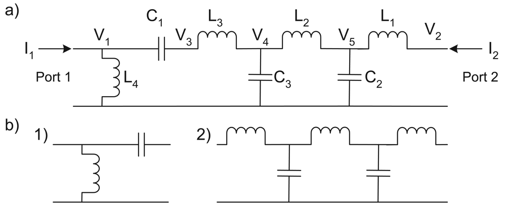
Figure 9.
(a) An alternative singly terminated network based around a cascade of Cauer stages; (b) Cauer network topologies: (1) a 2nd order high pass; (2) a minimum capacitance 5th order low pass network.
The Cauer network from Figure 9a in theory gives the same response as the original network from Figure 6 and being simply a cascade of simpler elements perhaps has a more obvious design procedure. The original network from Figure 6 is essentially derived from the fact that a shunt inductor is required at port 1 to give y11 the private pole that it requires, but the series capacitor realising the second transmission zero at s = 0 is free to be placed anywhere in the network, that is, in series with any of the floating inductors.
All of these networks (with the series capacitor in series with each different inductor) will give the correct form of the transfer function, but the simultaneous equations that need to be solved to derive the component values will be slightly different in each case. Indeed, for the case illustrated in Figure 9a no exact solution to the simultaneous equations has been found. The best solution found has component values:
| C1 | = | 133.3 mF |
| C2 | = | 68.5 mF |
| C3 | = | 504.1 mF |
| L1 | = | 400 mH |
| L2 | = | 18.3 mH |
| L3 | = | 48.3 mH |
| L4 | = | 13.4 mH |
The resulting Bode magnitude plot is also shown in Figure 8. Here it is noticed that the curvature of the magnitude response just below the passband is not the same as that for the wanted T(s) or that provided by the network of Figure 6. It is thus concluded that although the Cauer based network is feasible, and has a clearer design process, it is a less desirable arrangement. In principle, all of the different singly terminated networks could be generated and a further optimisation procedure used to select between networks, for example selecting the network with the most dynamic range [17], or the least component spread.
4. Doubly Terminated Design Procedure
To achieve the lowest sensitivity LC filter network a doubly terminated ladder, as illustrated in Figure 10, should be used. For the best results the source (Rs) and load (Rl) resistances are equal, and at this point are still assumed to be 1 Ω. The transfer function of this generic network is given by [12]
where

Figure 10.
A doubly terminated two port network with voltage mode transfer function.
Realising the correct transfer function thus now depends on realising the correct y22 in addition to y11 and y12.
It is possible to derive the required form of y22 using the Feldtkeller relation [12] but this is not considered in detail here. Instead the design proceeds by considering the singly terminated network and noting that the order between y11 and y22 can differ by at most one, due to the private pole at port 1. Also, to achieve the 7th order transfer function where all transmission zeros are at either zero or infinity the realisation of each y parameter will require no more than seven reactive elements.
Thus there can be at most one component to be added to port 2 of the network to realise the required transfer function. Given the form of the singly terminated network (Figure 6) there are four possible components:
- A series inductor;
- A shunt inductor;
- A shunt capacitor;
- No extra component required.
A series capacitor would simply alter the effective value of C1 and so is not suitable. Given these four possibilities, by finding the resulting transfer function of each case, simple elimination shows that in the case considered here no extra components are required. The required form of y22 is already satisfied, it is simply a matter of realising it numerically.
All four y parameters of the network of Figure 10 are thus now found and substituted into the transfer function (52). This results in generating the following parameters for the transfer function coefficients:
where for the minimum sensitivity implementation Rl = Rs = 1 Ω. Solving these equations with respect to the numerical values from (24) gives the component values
| C1 | = | 15.3 mF |
| C2 | = | 60.9 mF |
| C3 | = | 50.0 mF |
| L1 | = | 500.7 mH |
| L2 | = | 135.6 mH |
| L3 | = | 19.1 mH |
| L4 | = | 384.7 mH |
The resulting doubly terminated network is illustrated in Figure 11 and the Bode magnitude response in Figure 12. This network is exactly the same as Figure 7 but with a second terminating resistor and different component values. The wanted value of the centre frequency gain is again not realised and it is now found to be approximately −6 dB. Note that the maximum possible gain would be −3 dB due to the potential divider action of two resistors connected via a lossless LC network. A negative sign, corresponding to a 180° phase factor, is also introduced due to the parameter a not being found exactly.

Figure 11.
A minimum capacitor doubly terminated LC ladder realising the desired transfer function.
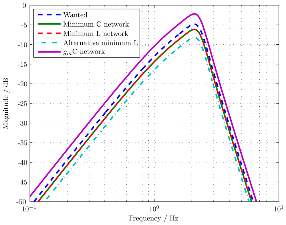
Figure 12.
Bode magnitude responses for the doubly terminated LC ladder networks. All the proposed networks match the wanted response well: the minimum capacitor network (Figure 11); the minimum inductor network (Figure 14); the alternative minimum inductor network (Figure 16); and the final gmC simulation of the LC ladder (Figure 17) assuming ideal transconductor elements.
5. Minimum Inductor Topology
The network of Figure 11 is canonical and a minimum capacitor realisation in that it forms a 7th order filter with three capacitors and four inductors. It is a minimum capacitor realisation as the core of the network is the 5th order Cauer low pass network illustrated in Figure 9b which has three inductors and two capacitors. In principle it is possible to replace this with a minimum inductor Cauer network as illustrated in Figure 13.
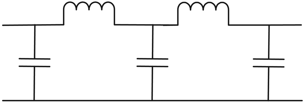
Figure 13.
A minimum inductor 5th order Cauer low pass network.
This is done by repeating the network synthesis procedure, but now in terms of the z, rather than y, parameters. These parameters are derived in terms of open circuit tests and so the private pole at port 1 becomes a series capacitor rather than a shunt inductor. This gives the minimum inductor implementation of the desired transfer function which is illustrated in Figure 14. Note that in principle L3 could be placed in parallel with any of the shunt capacitors and the same transfer function will be derived, subject to the satisfactory solution of the simultaneous equations. It is placed at the end of the network here to provide a direct dual to the minimum capacitance network of Figure 11 which has reasonable component values.

Figure 14.
A minimum inductor doubly terminated LC ladder realising the desired transfer function.
Analysing the network of Figure 14 by writing the nodal equations, performing Gaussian elimination using the
pivot function in Maple to derive the y parameters, inverting this matrix to give the z parameters, and substituting these values into the the z parameter equivalent of (52):
where
shows that the network does indeed have the correct transfer function. Solving the resulting simultaneous equations results in component values of
and the resulting Bode magnitude response is again shown in Figure 12.
| C1 | = | 384.7 mF |
| C2 | = | 19.1 mF |
| C3 | = | 135.6 mF |
| C4 | = | 500.7 mF |
| L1 | = | 50.4 mH |
| L2 | = | 60.9 mH |
| L3 | = | 15.3 mH |
Note that in on-chip implementations inductors generally cannot be realised directly Instead they are simulated using gyrators (see Section 7). These are the only active elements in an otherwise passive network. The number of inductors is thus ideally minimised to reduce the power consumption, and so only the the minimum inductor topology of Figure 14 is now considered.
6. Scaled Component Values
The component values for the network of Figure 14 have been derived for load resistances of Rs = Rl = 1 Ω. The resulting capacitor values are in the range of milli-Farads and inductances in the range of milli-Henrys. Obviously these values are impractical for circuit implementations. To overcome this the load resistances are now scaled to a value R. The capacitors and inductors required to realise the same transfer function then scale as
To make the maximum capacitance value equal to 30 pF, readily achievable on-chip, the value of R required is 16.7 GΩ. This corresponds to a conductance of 60 pS, which is challenging, but possible to make on-chip [24,25]. The required capacitor and inductor values then become
| C1 | = | 23 pF |
| C2 | = | 1.14 pF |
| C3 | = | 8.1 pF |
| C4 | = | 30 pF |
| L1 | = | 841.2 MH |
| L2 | = | 1.016 GH |
| L3 | = | 255.4 MH |
However, these inductor values are still not suitable for on-chip implementation, and have to be simulated with gyrators.
7. Gyrator Substitution
A final gmC filter structure is obtained simply by element substitution where each inductor in the LC network is replaced by a gyrator. It is noted that the alternative approach, operational simulation, is just a mathematical formalisation of the element substitution procedure, and the end results are in principle the same [26].
Many alternative gyrator circuits could potentially be used to replace the inductors in the circuit. For example, a floating inductor can be made with four single ended transconductors [13] or three single-ended transconductors [27]. The four transconductor version consumes more power, but has superior performance in the presence of noise and parasitic components [28]. Alternatively, a floating inductor can be made using two differential transconductors and a common mode feedback circuit [29], again giving a different power-performance trade-off.
Here the three transconductor variation is used and is illustrated in Figure 15a,b. For the grounded inductor the identity of Figure 15c from [30] is used as it applies the input voltage to two transconductors simultaneously. This provides an effective doubling of the input voltage and compensates for the unavoidable 3 dB passband attenuation that occurs between the two matched resistors. In all three cases
and
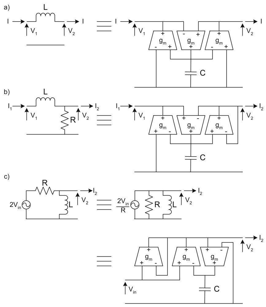
Figure 15.
Gyrators simulating inductors [27,30]. (a) A three transconductor gyrator simulating a floating inductor; (b) A three transconductor gyrator simulating a floating inductor and a shunt resistor; (c) A three transconductor gyrator providing input voltage doubling, voltage source to current source conversion and simulating a shunt inductor and resistor.
Unfortunately, the network form of Figure 14 developed so far cannot utilise the voltage doubling identity of Figure 15c as the source end is a capacitive potential divider and so no inductor is available to form the required gyrator. To overcome this the LC network is modified to the form of Figure 16 where the un-scaled component values are:
| Rs | = | 1Ω |
| Rl | = | 1Ω |
| C1 | = | 31.6 mF |
| C2 | = | 24.8 mF |
| C3 | = | 148 mF |
| C4 | = | 39.4 mF |
| L1 | = | 187.8 mH |
| L2 | = | 260.4 mH |
| L3 | = | 104.8 mH |

Figure 16.
The final doubly terminated LC ladder implementing (2). This is rearranged from the network of Figure 14 to provide a shunt inductor at port 1 of the network so that the voltage doubling identify of Figure 15c can be used.
This topology provides both the required transfer function (see Figure 12) and the inductor at the input node, and is a simple rearrangement of the existing network. Note, however, that there is no longer an explicit private pole at port 1. This was a requirement of the singly terminated network but is not essential for the doubly terminated network. Removing it though comes at the cost of introducing the series LC tank C2 and L2. The high Q of this network branch can be problematic to simulate and implement, occasionally leading to peaking in the filter transfer function. This is accepted here however, especially as the modified network has the advantage of having a reduced capacitance spread and increased transconductance compared to the original network (see below).
Substituting the identities into the network of Figure 16 the final gmC filter is shown in Figure 17. For all transconductances set at 100 pS the end capacitor values are:
which can readily be achieved on-chip. Again, due to the low 2.1 Hz centre frequency of the transfer function considered the transconductance required is low, at 100 pS, but can be realised [24,25]. Higher centre frequency filters will require higher transconductance values.
| C1 | = | 3.16 pF |
| C2 | = | 2.48 pF |
| C3 | = | 14.8 pF |
| C4 | = | 3.94 pF |
| CL1 | = | 18.8 pF |
| CL2 | = | 26.0 pF |
| CL3 | = | 10.5 pF |

The Bode magnitude response of the gmC network is shown in Figure 12 and the centre frequency gain of the filter is again changed and is now found to be a factor of −1.3511 larger than the wanted value. This gmC topology completes the synthesis of a doubly terminated LC ladder based filter that is suitable for on-chip implementation.
8. Conclusions and Algorithmic Summary
Filters based upon ladders of inductors and capacitors show inherently low sensitivity to non-exact component values; an essential design parameter for low power devices where robust operation is mandatory. For example, battery powered physiological monitors must be reliable, and must also operate at the very low frequencies associated with bodily phenomena whilst consuming very little power. Low frequency operation results in the presence of significant parasitic components and design in weak inversion for low power results in increased levels of device current mismatch, both making low sensitivity circuit design key.
Through the use of a detailed, high order, design example this paper has reviewed the procedure of LC ladder synthesis, making use of symbolic maths engines that can solve the non-linear simultaneous equations. Inevitably, in the space available it is not possible to consider and address all possible design issues that would potentially be of interest, but a clear overview has been provided. To conclude, the procedure considered in this article is summarised in Table 1 to aid in the design of other transfer function cases. This is presented for the minimum capacitor network case; the procedure for the minimum inductor network is identical, but based upon the z rather than y parameters.

Table 1.
Summary of the core procedure used in this article to aid in the design of other transfer function cases.
Supplementary Material
jlpea-01-00020-s001.pdfReferences
- Tsividis, Y.P. Integrated continuous-time filter design—an overview. IEEE J. Solid-State Circuits 1994, 29, 166–176. [Google Scholar]
- Haddad, S.A.P.; Bagga, S.; Serdijn, W.A. Log-domain wavelet bases. I IEEE Trans. Circuits Syst. I 2005, 52, 2023–2032. [Google Scholar]
- Odame, K.M.; Anderson, D.V.; Hasler, P. A Bandpass Filter With Inherent Gain Adaptation for Hearing Applications. I IEEE Trans. Circuits Syst. I 2008, 55, 786–795. [Google Scholar]
- Gosselin, B.; Sawan, M.; Kerherve, E. Linear-Phase Delay Filters for Ultra-Low-Power Signal Processing in Neural Recording Implants. IEEE Trans. Biomed. Circuits Syst. 2010, 4, 171–180. [Google Scholar]
- Vittoz, E.A. Future of analog in the VLSI environment. Proceedings of the IEEE International Symposium on Circuits and Systems, New Orleans, LA, USA; 1990. [Google Scholar]
- Enz, C.C.; Vittoz, E.A. CMOS low-power analog circuit design. Proceedings of the IEEE International Symposium on Circuits and Systems, Atlanta, GA, USA; 1996. [Google Scholar]
- Franco, S. Design with Operational Amplifiers and Analog Integrated Circuits, 3rd ed.; McGraw-Hill: London, UK, 2002. [Google Scholar]
- Johns, D.A.; Snelgrove, W.M.; Sedra, A.S. Orthonormal ladder filters. IEEE Trans. Circuits Syst. 1989, 36, 337–343. [Google Scholar]
- Sedra, A.S.; Brackett, P.O. Filter Theory and Design: Active and Passive; Matrix: Champaign, IL, USA, 1978. [Google Scholar]
- Darlington, S. A history of network synthesis and filter theory for circuits composed of resistors, inductors, and capacitors. IEEE Trans. Circuits Syst. 1984, 31, 3–13. [Google Scholar]
- Skwirzynski, J.K. Design Theory and Data for Electrical Filters; Van Nostrand: London, UK, 1965. [Google Scholar]
- Temes, G.C.; LaPatra, J.W. Introduction to Circuit Synthesis and Design; McGraw-Hill: London, UK, 1977. [Google Scholar]
- Schaumann, R.; van Valkenburg, M.E. Design of Analog Filters; Oxford University Press: Oxford, UK, 2001. [Google Scholar]
- Koller, R.D.; Wilamowski, B.M. A ladder prototype synthesis algorithm. Proceedings of the IEEE 35th International Midwest Symposium on Circuits and Systems, Washington DC, USA; 1992. [Google Scholar]
- lamowski, B.M.; Gottiparthy, R. Active and passive filter synthesis using Matlab. Int. J. Eng. Ed. 2005, 21, 561–571. [Google Scholar]
- Wanhammar, L. Analog Filters Using Matlab; Springer: Dordrecht, The Netherlands, 2009. [Google Scholar]
- Groenewold, G. Optimal Ladder Filters. IEEE Trans. Circuits Syst. II 2009, 56, 147–151. [Google Scholar]
- Jagiela, M.; Wilamowski, B.M. A methodology of synthesis of lossy ladder filters. Proceedings of the 2009 International Conference on Intelligent Engineering Systems, Barbados; 2009; pp. 40–50. [Google Scholar]
- Su, K.L. Analog Filters, 2nd ed.; Kluwer Academic: Norwell, MA, 2002. [Google Scholar]
- Casson, A.J.; Yates, D.C.; Patel, S.; Rodriguez-Villegas, E. An analogue bandpass filter realisation of the Continuous Wavelet Transform. Proceedings of 29th Annual International Conference of the IEEE Engineering in Medicine and Biology Society, Lyon, France; 2007. [Google Scholar]
- Homepage of Nuhertz Filter Solutions 2008. Available online: http://www.filter-solutions.com/ (accessed on 25 January 2011).
- Almost All Digital Electronics (AADE) filter design and analysis v4.42. Available online: http//www.aade.com/ (accessed on 25 January 2011).
- Casson, A.J.; Rodriguez-Villegas, E. Toward online data reduction for portable electroencephalography systems in epilepsy. IEEE Trans. Biomed. Eng. 2009, 56, 2816–2825. [Google Scholar]
- Becker-Gomez, A.; Cilingiroglu, U.; Silva-Martinez, J. Compact sub-Hertz OTA-C filter design with interface-trap charge pump. IEEE J. Solid-State Circuits 2003, 38, 929–934. [Google Scholar]
- Arnaud, A.; Galup-Montoro, C. Pico-A/V range CMOS transconductors using series-parallel current division. Electron. Lett. 2003, 39, 1295–1296. [Google Scholar]
- Schaumann, R. Simulating lossless ladders with transconductance-C circuits. IEEE Trans. Circuits Syst. II 1998, 45, 407–410. [Google Scholar]
- Geiger, R.L. Active filter design using operational transconductance amplifiers: A tutorial. IEEE Circuits Devices Mag. 1985, 1, 20–32. [Google Scholar]
- Banchuin, R.; Chaisricharoen, R.; Chipipop, B.; Sirinaovakul, B. In Depth Analysis of The CMOS OTA-Based Floating Inductors. Proceedings of IEEE International Symposium on Intelligent Signal Processing and Communication Systems, Yonago, Japan; 2006. [Google Scholar]
- Yuan, F. CMOS Active Inductors and Transformers: Principle, Implementation, and Applications; Springer: New York, NY, USA, 2008. [Google Scholar]
- Corbishley, P.; Rodriguez-Villegas, E. A Nanopower Bandpass Filter for Detection of an Acoustic Signal in a Wearable Breathing Detector. IEEE Trans. Biomed. Circuits Syst. 2007, 1, 163–171. [Google Scholar]
© 2011 by the authors; licensee MDPI, Basel, Switzerland. This article is an open access article distributed under the terms and conditions of the Creative Commons Attribution license (http://creativecommons.org/licenses/by/3.0/.)