Article

A Novel Inductorless Design Technique for Linear Equalization in Optical Receivers

by
Diaaeldin Abdelrahman
1,2,*,
Christopher Williams
3,
Odile Liboiron-Ladouceur
4 and
Glenn E. R. Cowan
2
1
Electrical Engineering Department, Faculty of Engineering, Assiut University, Assiut 71543, Egypt
2
Department of Electrical and Computer Engineering, Concordia University, Montreal, QC H3G 1M8, Canada
3
Nokia, New York, NY 10016, USA
4
Department of Electrical and Computer Engineering, McGill University, Montreal, QC H3A 0G4, Canada
*
Author to whom correspondence should be addressed.
J. Low Power Electron. Appl. 2022, 12(2), 19; https://doi.org/10.3390/jlpea12020019
Submission received: 27 December 2021 / Revised: 28 January 2022 / Accepted: 4 February 2022 / Published: 1 April 2022
(This article belongs to the Special Issue Low Power Memory/Memristor Devices and Systems)

Abstract

:
To mitigate the trade-off between gain and bandwidth of CMOS multistage amplifiers, a receiver front-end (FE) that employs a high-gain narrowband transimpedance amplifier (TIA) followed by an equalizing main amplifier (EMA) is proposed. The EMA provides a high-frequency peaking to extend the FE’s bandwidth from 25% to 60% of the targeted data rate f b i t . The peaking is realized by adding a pole in the feedback paths of an active feedback-based wideband amplifier. By embedding the peaking in the main amplifier (MA), the front-end meets the sensitivity and gain of conventional equalizer-based receivers with better energy efficiency by eliminating the equalizer stages. Simulated in TSMC 65 nm CMOS technology, the proposed front-end achieves 7.4 dB and 6 dB higher gain at 10 Gb/s and 20 Gb/s, respectively, compared to a conventional front-end that is designed for equal bandwidth and dissipates the same power. The higher gain demonstrates the capability of the proposed technique in breaking the gain-bandwidth trade-off. The higher gain also reduces the power penalty incurred by the decision circuit and improves the sensitivity by 1.5 dB and 2.24 dB at 10 Gb/s and 20 Gb/s, respectively. Simulations also confirm that the proposed FE exhibits a robust performance against process and temperature variations and can support large input currents.

1. Introduction

Traffic in data centers has grown rapidly over the past decade due to the rapid growth of cloud computing and big data applications. This in turn drives the development of robust, high-speed, and energy-efficient interconnects to transfer the data around the data center. Several 100+ Gb/s optical links have recently been reported to satisfy the bandwidth and reach requirements [1,2,3]. However, the associated cost and power dissipation prevent their widespread adoption within the data center. In short-reach photonic links, the transmitted optical modulation amplitude (OMA) must be sufficiently large that, in spite of coupling and fiber losses, the received optical power exceeds the receiver’s sensitivity limit. This sensitivity is a function of the input-referred noise current of the receiver as well as the voltage amplitude requirements of the decision circuit driven by the receiver front-end [4]. Therefore, an energy-efficient link design requires a low-noise as well as a high-gain receiver.
As data rates increase, traditional approaches to receiver design dictate that the bandwidth of the receiver also increases, which limits the maximum achievable gain [5]. This trade-off is less pronounced in SiGe BiCMOS technologies where the transistor has higher intrinsic gain and transit frequency. Therefore, a reasonable gain is still achievable in wideband deigns. However, in CMOS, the trade-off limits the per-stage gain which necessitates cascading several gain stages to achieve the targeted output voltage amplitude. With increased number of stages, both noise and power dissipation increase.
This paper presents a novel inductorless design technique for high-gain optical receiver front-ends. Figure 1 illustrates the operation of the proposed front-end (FE) in contrast to the traditional wideband FE. Conventionally, the transimpedance amplifier (TIA) and the follow-on main amplifier (MA) are designed to have bandwidths in the order of 0.6 f b i t and f b i t , respectively, to achieve an overall bandwidth of approximately 0.5 f b i t [4]. In the proposed receiver, first, the TIA’s bandwidth is reduced to approximately 25 % of the targeted data rate. The reduced TIA bandwidth allows for higher gain, lower input-referred noise, and fewer follow-on gain stages. The reduction in bandwidth also introduces inter-symbol interference (ISI) to the extent that the TIA’s output eye diagram is fully closed. Unlike a bandlimited electrical channel which can introduce more than 30 dB of channel loss at the Nyquist frequency f N = 0.5 f b i t , the low-bandwidth TIA introduces a moderate frequency-dependent attenuation. Consequently, a few dBs of amplitude peaking at fN is sufficient to restore the required bandwidth (for example, the equalizer in [6] introduces only 7 dB of peaking). Therefore, in the second step of the proposed design technique, a high-frequency peaking is intentionally introduced in the main amplifier’s amplitude response without impairing its low-frequency gain. Various possible designs of active feedback-based MA architectures [7,8,9,10] can introduce the required peaking by adding a pole in their feedback loops. The amplitude peaking in the equalizing main amplifier (EMA) is then used to compensate for the TIA’s limited bandwidth to restore an overall bandwidth of approximately 0.5 f b i t . Although Figure 1 shows only the magnitude response of the TIA and EMA, group-delay variation must also be considered.
In contrast to traditional continuous-time linear equalizer (CTLE)-based designs [6,11], the proposed front-end attains the improved sensitivity and high-gain of these designs, while achieving better energy efficiency due to the elimination of the standalone equalizer stage(s). Traditional approaches to CTLE design, based on RC degenerated common-source amplifiers, suffer from a limited bandwidth and consequently insufficient peaking at high frequencies. When CTLEs are cascaded the reduction in overall bandwidth due to repeated real poles follows the same trend as that of 1st-order gain cells. Further, a 1st-order CTLE stage has a limited capability in equalizing a second-order TIA [6,12] which necessitates cascading several equalizer stages, further increasing power and area overheads. On the other hand, various inductorless feedback techniques can be used to design main amplifiers with gain-bandwidth products (GBW) far superior to a cascade of first-order stages [7,8,9,10]. The improvement is the result of poles moving away from the negative real axis. A combination of poles with high- and low-quality factors gives better GBW for the same pole magnitude. The proposed approach to design an EMA improves the overall receiver performance by increasing the gain of the TIA and improving noise performance as argued [6], but with the wideband performance of state-of-the-art MA designs.
The proposed design technique requires co-designing the TIA and the subsequent equalizing amplifier. Therefore, both stages receive equal attention in the analysis. Section 2 in this paper provides a detailed analysis of the TIA, highlighting the trade-off between its gain and bandwidth. Section 3 introduces the concept and the block diagram of the proposed EMA. The performance of the overall FE (TIA/EMA) is studied in Section 4. Section 5 shows the circuitry and simulation results of the proposed FE in comparison to the conventional full bandwidth design. Finally, Section 6 concludes the work.

2. Transimpedance Amplifier

2.1. Small-Signal Model and Freuqency Response

The inverter-based TIA (Inv-TIA) is used in this work due to its superior noise performance over its common-gate (CG) counterpart. Further, unlike the CG-TIA, the Inv-TIA is a self-biased topology which decouples the gain from the transconductance of the input device and allows for performance optimization without being limited by DC biasing constraints. The circuitry and the small-signal model of the Inv-TIA are shown in Figure 2. The CMOS inverter is modeled by its total transconductance g m and output resistance R A . Therefore, the core voltage amplifier has an open-loop transfer function of A c o r e s = A 0 / 1 + s T A , where A 0 = g m R A is the DC voltage gain and T A is the time-constant formed by the output resistance R A and the total output capacitance C L . In the model, C T is the total input capacitance, including both the photodiode capacitance C D and the circuit’s input capacitance C I . Considering this model, the Inv-TIA exhibits a second-order transfer function characterized by a natural oscillation frequency ω 0 , a pole quality factor Q 0 , and a midband transimpedance gain of Z T I A , 0 R F [13]. The natural oscillation frequency ω 0 is converted to the corresponding TIA’s 3dB-bandwdith f T I A through a coefficient ρ that depends on the shape of the TIA’s amplitude response (i.e., ρ is a function of Q 0 ). Detailed expressions for ω 0 , Q 0 , and ρ can be found in [14].
In the Inv-TIA, A 0 is constant for a given biasing condition, fixed ratio of W p / W n , and technology node. For example, an inverter with V D D = 1   V ,   W n = W p , and simulated in TSMC 65 nm CMOS technology achieves A 0 of 6   V / V . Further, the gain-bandwidth product of the core amplifier G B W A = A 0 / 2 π T A is also constant. The circuit’s input capacitance C I is determined by the total transistor width and is usually chosen as a fraction of the photodiode capacitance based on the noise and power constraints [14]. Therefore, for a given C D , once C I is fixed, the TIA’s performance is controllable only through the feedback resistor. In this work, unless mentioned otherwise, A 0 , G B W A , and C T are set to 6   V / V , 75   GHz , and 200   fF , respectively.
Figure 3a shows that both the 3 dB bandwidth and the pole quality factor Q 0 decrease with larger feedback resistor R F . The bandwidth degrades almost linearly with the feedback resistor. In fact, the bandwidth does not follow the square-law relation R F   α   f T I A 2 predicted by the Transimpedance Limit [13]. This discrepancy can be explained as follows: Unlike [13], the model in this work allows Q 0 to change with R F   Q 0 = A 0 + 1 R F C T T A / R F C T + T A . For sufficiently large R F that makes R F C T   T A , Q 0 is proportional to R F 0.5 . Consequently, it is reasonable to assume that ρ is also proportional to R F 0.5 with a percentage error of less than ± 8 % , as shown in Figure 3b. Using this relation to rearrange the transimpedance limit from [13]:
f T I A 2 = A 0 + 1 A 0 G B W A   ρ 2 2 π R F C T
which implies:
f T I A 2     1 R F 2       f T I A     1 R F  
This means that changing R F changes both the pole magnitude ω 0 and the pole quality factor Q 0 which modifies the bandwidth dependency on the feedback resistor from that given in [13] where Q 0 is assumed to be constant. Assuming a constant Q 0 when R F is increased by a factor of r requires both A 0 and T A to scale up by a factor of r . Practically, this approach is not feasible since the voltage gain of a single-stage CMOS inverter is constant for a given biasing and its maximum value is limited by the technology node.

2.2. Effective Gain

When f T I A is reduced far below f b i t , severe ISI is introduced to the extent that the output eye diagram is fully closed. Therefore, the DC value of Z T I A s becomes a deceptive measure of the gain. The effective gain must be calculated from the transient response; more precisely, from the pulse response [15]. The TIA’s pulse response is the response to an isolated binary one transmitted in a long sequence of binary zeros. Assuming a linear time-invariant (LTI) operation, if the TIA’s response to a step input with a peak-to-peak value of i p p is defined as x t , then its pulse response is calculated as y t = x t x t U I , where UI is the unit interval. The output pulse response of the Inv-TIA is plotted in Figure 4a for a data rate of 10   Gb / s with i p p = 10   μ A pp and a bandwidth ranging from 0.2 f b i t to 0.6 f b i t . To quantify the ISI, y t is sampled at the symbol rate relative to its peak (as shown by the marker points in Figure 4a), resulting in a discrete-time sequence V h , n given by:
V h , n = y n T b                                 < n <
The sample at the peak of the pulse is denoted as the main-cursor sample V h , 0 . An effective gain of Z h , 0 can be interpreted as V h , 0 / i p p if all ISI is cancelled. In the absence of equalization, the ISI samples ( V h , n 0 ) can be subtracted from V h , 0 , closing the vertical eye opening ( V E O ) to:
V E O = V h , 0 n = n 0 V h , n
The effective gain is calculated based on the receiver architecture as follows: 1. The VEO can be used to determine an effective gain of Z V E O = V E O / i p p for the case in which the ISI is not removed or is only partially removed. The midband gain Z T I A , 0 can also be interpreted as an effective gain if an ideal unity-gain continuous-time linear equalizer (CTLE) is employed. The CTLE compensates for the bandwidth limitation of the TIA and restores an overall bandwidth on the order of 0.6 f b i t without impairing the low-frequency gain. Therefore, the TIA’s midband gain Z T I A , 0 at the low bandwidth point can be used as the effective gain for the combined (TIA/CTLE).
Figure 4b shows that linear equalization improves the effective gain over both full-bandwidth and ISI canceller-based designs. For example, if the TIA’s bandwidth is reduced from 0.6 f b i t (point a) to 0.3 f b i t and an ideal CTLE is employed (point b), the effective gain improves by a factor of 1.86× compared to point a. The gain at 0.3 f b i t (point b) is also 1.23× larger than that where an ideal ISI-canceller is employed (point c). That is, ISI cancellers have no bearing on the TIA’s bandwidth which means that the output pulse of a limited-bandwidth TIA does not have enough time to settle at the voltage value i p p Z T I A , 0 . Further, ideal cancelers that remove all pre- and post-cursor ISI are not implementable. For example, decision feedback equalizers (DFEs) [12] cancel only the post-cursor ISI. DFEs also suffer from a tight timing constraint where the feedback signal from the previously decided bit must arrive within one unit interval (UI) to resolve the current bit. These limitations make linear equalization a more attractive choice for applications that require high gain in the receiver FE. DFEs, on the other hand, are favorable over CTLEs from the noise point of view. That is, CTLEs extend the noise bandwidth to be a function of the bandwidth of the combined TIA/CTLE instead of being a function of the bandwidth of the low-bandwidth TIA as in the DFE-based receivers [15]. Therefore, a fair comparison between different receiver architectures should consider more complete figures of merit, such as OMA sensitivity and energy efficiency. The noise performance of the presented front-end is carefully examined in Section 4.3 in the presence of the equalizing main amplifier.

3. Equalizing Main Amplifier

In addition to high-gain and broadband operation, adjustable high-frequency peaking (HFP) is a desirable feature in MA design. The amplitude peaking at the Nyquist frequency can mitigate the bandwidth limitation introduced by other components in the optical link. For example, in [16], shunt and series passive inductors are employed between cascaded stages of a programmable gain amplifier to realize an HFP. The HFP is then used to partially compensate for the varying performance of the multi-mode fiber. In this work, passive inductors are avoided because they consume significant silicon area and potentially increase substrate coupling. The HFP is realized by introducing a pole in the feedback loop of an active feedback-based MA architecture and used to compensate for the TIA’s limited bandwidth.

Equalizing MA Based on a Third-Order Gain Stage

The block diagrams of the conventional and proposed gain stages are shown in Figure 5a,b, respectively. The conventional architecture is presented in [17], where a third-order nested feedback technique achieves high-speed operation while maintaining robust stability compared to the traditional third-order gain stage. In the block diagram in Figure 5a, the first-order gain cell, A s , is modeled by the transconductance of the input device g m 1 , load resistance R 1 , and load capacitance C 1 . The adjustable active feedback β c o n s cell is modeled by the transconductance g m f . Therefore, the transfer functions of the first-order gain and feedback cells are given by:
A s = A 1 s ω 1 + 1 ,                     β c o n s = β 1 s ω 1 + 1 ,  
where A 1 = g m 1 R 1 and ω 1 = R 1 C 1 1 are the DC gain and cut-off frequency of the first-order gain cell, respectively. β 1 = g m f R 1 is the DC feedback gain. The transfer function of the overall architecture in Figure 5a is given by:
H M A s = A 3 s A 2 s β c o n s + A s β c o n s + 1
In this work, two poles are introduced in the feedback loops to create an adjustable HFP without impairing the low-frequency gain. The transfer function of the proposed EMA is calculated using (5) by replacing β c o n s by β P r o given in (6):
β p r o s = β 1 s ω 1 + 1 s ω Z + 1
where ω Z = R Z C Z 1 is the cut-off frequency of the introduced low-pass filter which is assumed to have negligible loading on the output node. Therefore, the transfer function of the EMA in Figure 5b is given by:
H E M A s = A 1 3   s ω Z + 1 s ω 1 + 1 3 s ω Z + 1 + A 1 β 1 s ω 1 + 1 + A 1 2 β 1
The pole-zero locations of (7) are plotted in Figure 6a in comparison with that of (5) for β 1 , A 1 , and ω 1 , fixed at 0.25, 2.5 , and 2 π × 30   GHz , respectively. The poles of the conventional architecture are indicated by black x-markers. For the proposed EMA, ω Z is swept from 0.5 ω 1 to 5 ω 1 . The insertion of the LPF in the feedback loops of the proposed EMA creates a real zero at ω Z (shown in blue). It also increases the order of the denominators of β p r o s and H E M A s compared to their conventional counterparts. As a result, for low values of ω Z , the proposed EMA has two sets of complex-conjugate poles P A   and   P B (shown in red). As ω Z increases, P A travels toward the complex poles of (5) while the damping factor of   P B increases until the two poles become real and start traveling in opposite directions. At sufficiently high ω Z ,   P B 2 and the real zero cancel each other,   P B 1 reaches the real pole of (5) and the overall architecture degenerates to the third-order gain stage in [17].
The impact of varying ω Z on the amplitude response of the proposed EMA is depicted in Figure 6b. For a given β 1 , HFP can be introduced independent from the low-frequency gain. The peak of the amplitude response moves to a lower frequency as ω Z is reduced. As a numerical example from Figure 6b, for ω Z = 0.1 ω 1 , the EMA achieves amplitude peaking of 6   dB at 5   GHz and increases to 10.5   dB at 11   GHz . In the presence of such high amplitude peaking, it is not instructive to explore the bandwidth of the EMA. Instead, the bandwidth extension ratio and the signal integrity are inspected in the following section for the overall front-end which includes the limited-bandwidth TIA and the EMA.

4. Front-End Performance Analysis

4.1. Performance Requirements for the EMA

The noise-limited input signal produces a peak-to-peak voltage of V O P P = S N R   i n , i n r m s   Z T I A , 0   A E M A , 0 at the output of the front-end, assuming that the EMA restores a wide overall bandwidth, where S N R is the required signal-to-noise ratio and is equal to 14.07 for a BER of 10 12 [4], i n , i n r m s is the input-referred noise current, and A E M A , 0 is the DC gain of the EMA. V O P P is sufficiently large to drive an ideal clock-and-data recovery (CDR) circuit to achieve the desired BER. However, the decision circuit in a realistic CDR has finite sensitivity and requires a minimum input voltage amplitude V C D R P P . Therefore, the FE’s output voltage needs to be increased by V C D R P P to attain the same BER as an ideal CDR. The finite sensitivity of the CDR incurs a power penalty ( P P ) of:
P P = V O P P + V C D R P P V O P P = 1 + V C D R P P S N R   i n , i n r m s   Z T I A , 0   A E M A , 0
The optical power incident to the photodiode, the electrical current generated from the photodiode, and the voltage produced at the output of the main amplifier are linearly proportional. As a result, the amount of additional optical power required to overcome any nonideality (power penalty) can be expressed in voltage terms as shown in (8). The equation reveals that higher transimpedance gain relaxes the gain requirements for the EMA for a given PP. Figure 4b shown earlier indicates that reducing the ratio f T I A / f b i t is beneficial for the gain as long as the equalizer is able to recover an overall bandwidth of approximately 50% to 60% of the targeted data rate. Therefore, the equalizer’s capability in restoring the bandwidth determines how far the TIA’s bandwidth can be reduced below the data rate. That is, excessive reduction of the TIA’s bandwidth would require the equalizer to introduce a large amount of amplitude peaking which translates into large group delay variation (GDV). The latter causes horizontal and vertical eye closure which reduces the gain and noise improvements gained from equalization. In [6], it is concluded that the equalizer can restore the bandwidth by a factor of approximately 2 × while simultaneously maintaining a good noise performance and a good quality of the equalized eye diagram.
For the conventional wideband TIA, a feedback resistor of 1.25   k is chosen to achieve a bandwidth of 0.57 f b i t , sufficiently large to introduce no ISI. The TIA’s bandwidth drops almost linearly with R F as observed in Figure 3a. Therefore, in the proposed design, the value of the feedback resistor is doubled, leading to a bandwidth of 0.26 f b i t . At this bandwidth, the TIA achieves a Z T I A , 0 of 66.6   dB   2143   while introducing an attenuation of 7.2   dB at the Nyquist frequency f N = 0.5 f b i t = 5   GHz . The EMA is now required to recover the bandwidth by a factor ranging from 1.9 × to 2.3 × to achieve an overall bandwidth on the order of 50 % to 60 % of f b i t . For example, using the gain of the low-bandwidth TIA while assuming V C D R P P , S N R , and i n , i n r m s of 50   mV pp , 14.07 , and 1   μ A rms , respectively, the PP defined in (8) can be used to calculate the required gain of the EMA. In addition to recovering the bandwidth, the EMA is required to amplify the TIA’s output by a low-frequency gain of approximately 20   dB to reduce the PP to less than 0.67   dB   1.17 . Practically, the EMA’s gain is determined to reduce the PP to a pre-determined value obtained from link budget analysis.

4.2. Bandwidth Extension and Signal Integrity

Figure 7 shows the block diagram of the proposed front-end where the limited-bandwidth TIA is followed by a two-stage EMA. The EMA’s second stage is added to relax the gain requirements. The two-stage EMA is modified based on the two-stage MA presented in [10] by inserting low pass filters in the feedback loops of the second stage. Therefore, the transfer function of the overall front-end (FE) is given by Z F E s = Z T I A s H 2 E M A s , where H 2 E M A s is the transfer function of the two-stage EMA and given by:
H 2 E M A s   = A 5 s D e n s
The denominator D e n s is expressed as:
D e n s = 1 + A s β c o n s + β p r o s + A 2 s β c o n s + β p r o s + β c o n s β p r o s + A 3 s β c o n s β p r o s
Once the TIA’s feedback resistor is fixed, the full design space is reduced to only two variables: ω Z and β 1 . These two variables are swept, and the following equations are solved numerically to calculate the bandwidth f F E , the low-frequency gain Z F E , 0 , and the peaking M p of the overall FE:
Z F E 2 π f F E = 1 2 Z F E j ω ω = 0
Z F E , 0 = 20 log 10 Z F E j ω ω = 0
M P = 20 log 10 max Z F E j ω Z F E j ω ω = 0
Several combinations of β 1 and ω z can achieve the required bandwidth extension but with different noise performance. The noise analysis is presented in the following section. The feedback gain β 1 directly impacts the low-frequency gain of the EMA and is chosen to satisfy the power penalty condition indicated earlier. Then, ω z is swept to achieve the required bandwidth extension ratio defined as f F E / f T I A . The pairing of ω z = 0.075 ω 1 and β 1 = 0.25 is chosen as it achieves a good noise performance as well as a good quality of the output eye. The corresponding frequency response is plotted in Figure 8a, where the EMA introduces 5 dB of peaking and extends the bandwidth by a factor of 2.2 × . The gain peaking in the overall frequency response is less than 0.1   dB . Figure 8b shows the pulse response at the output of the FE. To quantify the vertical and horizontal eye openings, the output pulse is sampled at a bit rate clock relative to its peak. The pulse is sampled at both the rising and falling edges of the clock. The sum of the magnitude of the samples at the even clock edges (filled markers for n 0 ) quantifies the ISI. The sum of the samples at the odd clock edges (hollow markers) is considered as a jitter indicator (JI). Note that the falling edges of the clock are the zero-crossing points of the data. Therefore, the defined JI includes only the deterministic jitter caused by the residual ISI or ringing in the time domain [18]. The sum of ISI and JI samples is less than 6.5 % of the main cursor sample which implies that the eye has a wide internal opening area, as evident also from the eye diagram in Figure 9a, obtained through simulation. Figure 9b shows the output eye diagram when the limited bandwidth TIA is followed by a wideband MA. The comparison between the two eyes in Figure 9 demonstrates the capability of the presented technique in restoring the bandwidth without impairing the midband gain or increasing power dissipation.

4.3. Noise Analysis

Figure 10a shows the model used for noise analysis. The main noise sources in the Inv-TIA are the channel and feedback thermal noise, shown in Figure 2 and Figure 10 as I n , c h 2 and I n , R F 2 , respectively. The power spectral densities of these two sources can be expressed as: I n , c h 2 = 4 k T γ g m and I n , R F 2 = 4 k T / R F where k is the Boltzmann constant, T is the temperature in Kelvin, and γ is the excess noise factor. Under a constant gain-bandwidth product constraint, the noise-optimum FET size is C I = 0.7 C D [14]. Therefore, the transconductance of the TIA’s input device can be calculated as g m = 2 π f T C I , where f T is the technology transit frequency at the selected bias point. In Figure 10a, the amplifier following the TIA is modeled by H p o s t s and its input-referred noise PSD is denoted by V n , i n 2 = 4 k T / g m , p o s t . H p o s t s is given by (9) and (10) for both the proposed and conventional designs, using β p r o s and β c o n s , respectively. In simulations that follow, g m , p o s t , γ , and f T are fixed at 10   m 1 , 2 , and 150   GHz , respectively.
Linear equalization extends both the signal and the noise bandwidths [15]. Therefore, the integration of the noise power spectral density (PSD) must be performed at the receiver output to take into consideration how the equalizer processes the noise. To do so, the contribution to the output noise PSD from each noise source is first calculated. Because all noise sources are uncorrelated, the total output noise PSD is constructed by adding up all individual power spectra. The total output noise PSD is then integrated up to infinity to calculate the integrated output-referred noise power v n , t o t a l 2 having units of V 2 . The total integrated input-referred noise power i n , t o t a l 2 in units of A 2 is then determined by dividing the v n , t o t a l 2 by the squared effective gain Z T I A , e f f 2 calculated from the VEO at the output of the FE. This gain calculation accounts for the residual ISI in the signal presented to the decision circuit. The input-referred noise current is then calculated as the square root of i n , t o t a l 2 . Further discussion about the noise analysis for equalizer-based optical receivers is available in our previously published work [15].

4.4. Performance Comparison

To assess the improvement of the proposed FE versus its conventional counterpart, both FEs are simulated in Matlab. The traditional FE has the same block diagram as in Figure 7 without the pole insertion in the feedback loops. Therefore, its analysis is the same as presented earlier, but replacing each β p r o s in (10) with β c o n s . The value of the TIA’s feedback resistor is tuned to set the ratio of f T I A / f b i t to 0.57 and 0.26 for the conventional and the proposed FEs, respectively. In the latter, the values of β 1 and ω Z are chosen to achieve an overall bandwidth of f F E = 0.56 f b i t . The power consumption and the DC gain of the proposed EMA are kept equal to that of the conventional MA by fixing the values of A 1 and β 1 in both circuits. The performance of the two FEs is summarized in Table 1. Although the two FEs have approximately the same overall bandwidth, the proposed FE achieves 6   dB higher gain compared to its conventional version. This improvement in the transimpedance gain resulted from the increased value of R F for the limited-bandwidth TIA. It is worth mentioning that this gain improvement comes without any additional power dissipation because changing R F and ω Z does not affect the DC power dissipation as will be shown in the practical implementation in the next section.
The input-referred noise power of both FEs is compared in Figure 10b. In the proposed FE, the feedback resistor and the post amplifier noise powers are improved compared to their counterparts in the conventional design. That is, increasing the value of R F in the proposed FE reduces its thermal noise contribution and increases the input-referral gain which suppresses the noise from the follow-on amplifier. The channel noise is slightly increased in the proposed FE due to HFP that amplifies the high-frequency noise. Overall, the presented design technique reduces the input-referred noise current by 11.2 % . The lower noise and higher gain in the presented FE led to 0.52   dB and 0.61   dB improvements in the noise-based sensitivity and the PP compared to the traditional design.

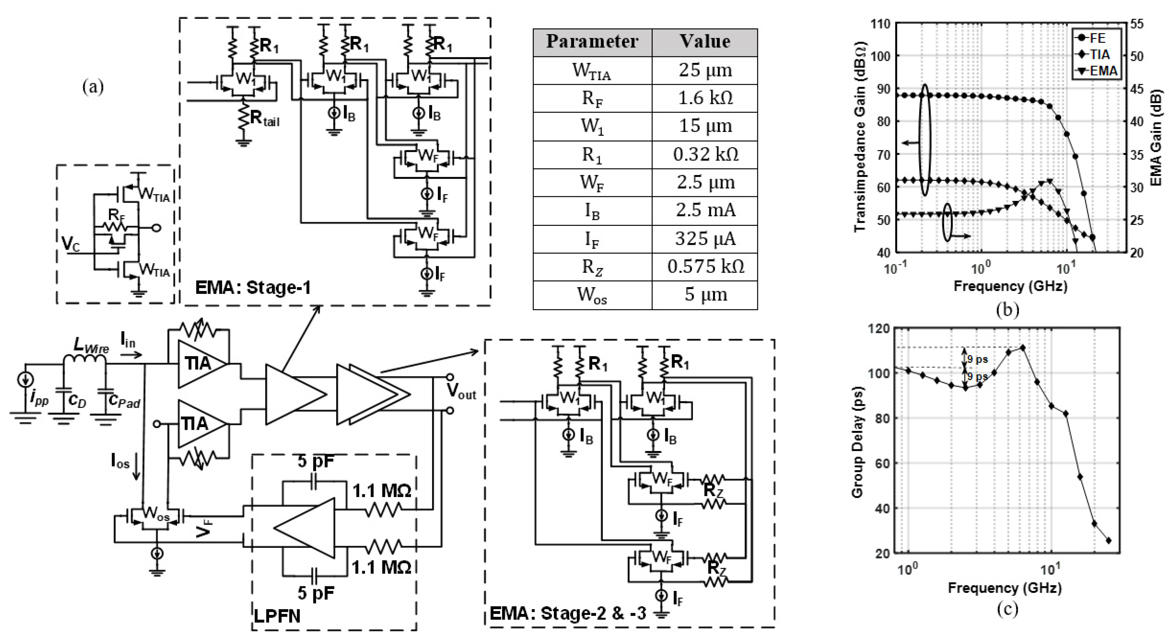
5. Circuitry and Layout of the Implemented Front-End

Figure 11a shows the block diagram and the circuitry of the implemented front-end. A replica TIA is used to provide pseudodifferential power-supply noise rejection. The TIA is followed by a three-stage EMA. A series resistor R Z is inserted in the feedback loops of the second and third stages. This resistor, in combination with the parasitic capacitance of the transistor in the feedback loops, creates the zero required for bandwidth extension. Compared to Figure 7, the EMA’s third stage is added to relax the gain requirements and assist in recovering the bandwidth. A low-pass feedback network (LPFN) is connected between the output of the EMA and the input of the TIA. The LPFN amplifies the difference between the DC levels at V O u t and returns a feedback voltage of V F that is then converted to a current I o s by the transconductance of M o s and subtracted from the input current for offset compensation. The LPFN is a single-pole RC filter using a Miller-boosted 5   pF capacitor and a 1.1   M resistor. A low cut-off frequency of 1   MHz is achieved as a trade-off between the on-chip area and the tolerable baseline wander for long runs of consecutive identical digits. The low common-mode voltage at the TIA’s output prevents the use of a tail current source for the first differential pair in the EMA’s first stage and therefore a poly silicon resistor is used instead.
The FE is simulated in TSMC-65 nm using a Cadence Spectre simulator. The input parasitics are modeled by a pad capacitance C P a d of 45   fF , a photodiode capacitance C D of 80   fF and a bondwire inductance L w i r e of 0.5   nH . The loading from the subsequent output buffer is modeled by a load capacitance of C L = 150   fF connected at the output of the EMA. An additional 50   fF capacitance is added to all nodes to model the wiring and layout parasitic. The receiver’s output stage (not shown in Figure 11a) is a conventional differential amplifier with a load resistance of 100   chosen as a trade-off between output signal amplitude and compatibility with the off-chip 50   environment.
Figure 12 shows the chip layout in TSMC 65 nm CMOS technology. The chip includes two standalone FEs. One FE is the direct implementation of the circuit in Figure 11a while the other is its conventional version (i.e., R Z is replaced by a short circuit). The total size of the chip is 1   mm × 0.7   mm . Each front-end is pad limited and occupies 665   μ m   × 460   μ m   0.31   mm 2 , including the I/O RF pads, while the active area, including the offset compensation loop, is about 0.0114   mm 2 . The high-speed RF input and output probing pads are differential G-S-G-S-G since each FE has differential inputs and outputs. The TIA, the MA/EMA, and the output buffer are powered by different supplies.

5.1. Validation of Bandwidth Extension

Similar to the previous section, both the proposed and the conventional FEs are simulated and compared. The proposed FE’s TIA bandwidth is 27 % of the targeted 10   Gb / s data rate. The tail current source in the feedback pair I F sets the feedback gain β 1 and is chosen to satisfy the power penalty condition. The series resistor R Z is then chosen to achieve the required bandwidth extension. The device dimensions and component values are tabulated in Figure 11a for nominal 10   Gb / s operation. All transistors in the signal and feedback paths use minimum length. Current sources, however, employ transistors with longer than minimum length. The corresponding amplitude responses are shown in Figure 11b. The EMA introduces a peaking of 4.8 dB at the Nyquist frequency and restores the bandwidth by a factor of 2.28 × , achieving an overall bandwidth of 6.1   GHz .
The simulated group-delay is also shown in Figure 11c where the GDV is within ± 10 % of the unit interval over the frequency range of interest. Figure 13a,b shows the 10   Gb / s eye diagrams at the output of the FE when the limited-bandwidth TIA is followed by a wideband MA or by the EMA, respectively. The eye diagrams obtained through simulation demonstrate the capability of the proposed peaking technique in restoring the bandwidth without impairing the low-frequency gain. The bandwidth extension improves the VEO by a factor of 1.7 × . Figure 13c shows the eye diagram of the traditional FE. In this simulation, R Z is shorted and R F is reduced to widen the TIA’s bandwidth while the current sources I F   and   I B are unchanged. Comparing Figure 13b,c shows that the presented design technique improves the effective gain by a factor of 2.34 × . Interestingly, for the proposed design, the gain is improved by almost the same amount as the TIA’s bandwidth is reduced. This emphasizes the linear relation between the gain and the bandwidth in the single-stage Inv-TIA. Table 1 summarizes the simulated performance of the two FEs where the presented FE shows 1.5   dB better sensitivity compared to its conventionally designed counterpart.

5.2. Sensitivity to Process and Temperature Variations

Figure 14 shows the simulated performance of the presented receiver under process and temperature variations. Figure 14a shows that the EMA exhibits more peaking at a lower temperature. For a given temperature, the peaking can vary by up to 6.5 dB over different process corners. The FE gain and bandwidth in Figure 14b can vary up to 13.5 dB and 3.4 GHz over different corners, respectively. The gain and bandwidth variations relative to their values at room temperature reach up to 24.3% and 22.5%, respectively, as the temperature varies from 20 to 80 . This performance variation is mainly caused by the constant current sources used in this design and can be counteracted by employing temperature-compensated or constant-gm biasing techniques [19]. Adaptation techniques can be also employed to continuously monitor the output eye diagram and set the circuit parameters accordingly to maintain the best quality for the equalized eye [20]. In the implemented prototype, the TIA’s feedback resistor and current sources in the forward and feedback paths are made variable. This allows for post-fabrication control on peaking frequency, peaking magnitude, and the TIA’s high-frequency roll-off. Therefore, the amplitude responses of both the EMA and the TIA track each other to achieve the targeted bandwidth with minimal GDV.
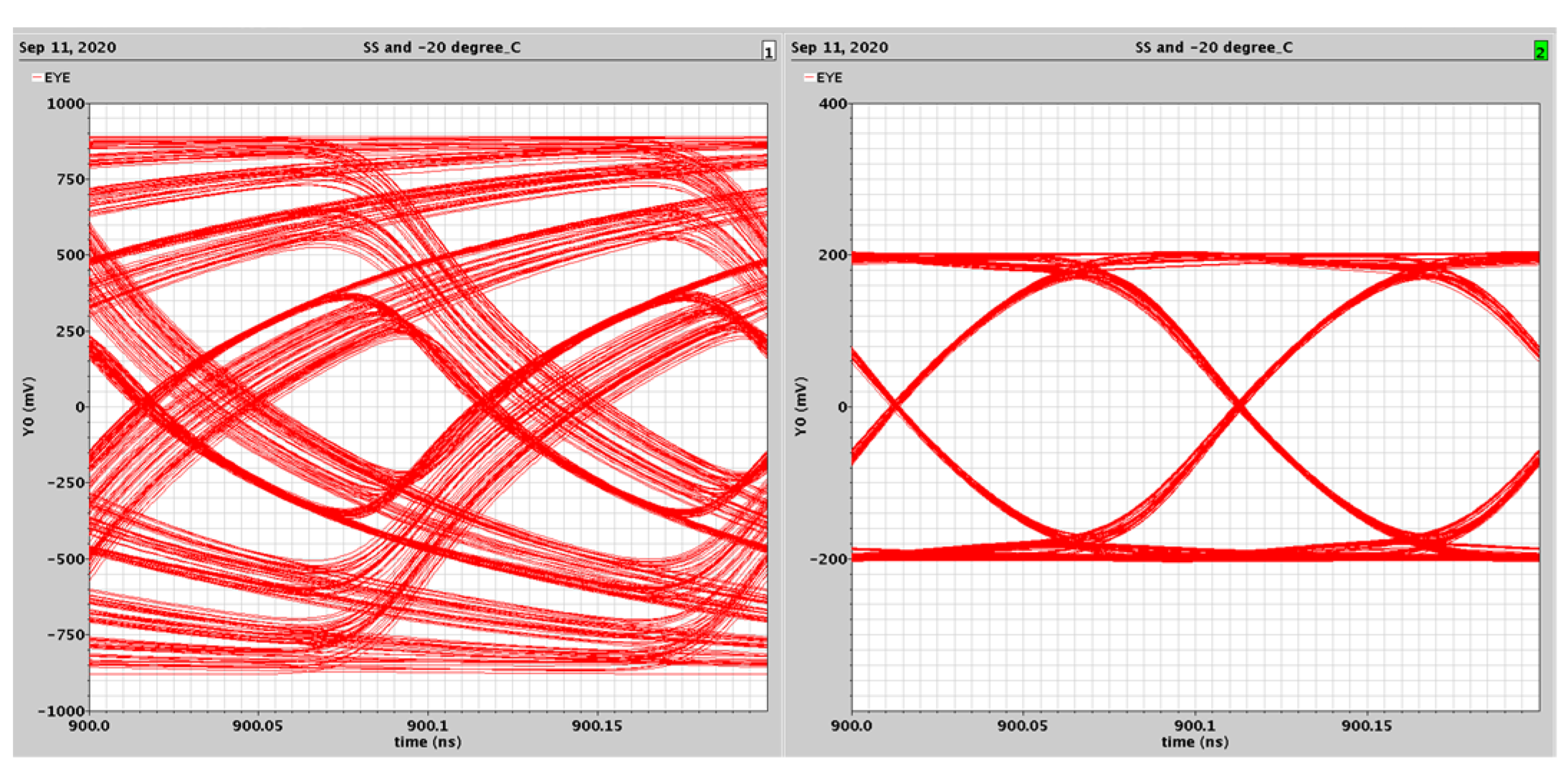
To prove that the proposed technique works despite the PT variations, Figure 15 shows the simulated 10 Gb/s eye diagram at the SS process corner and 20   . The uncompensated eye (left) shows a significant distortion. By carefully adjusting the circuit parameters, a clean eye is obtained (right) with an internal opening similar to that obtained under nominal operations. To generate the eye on the right, the circuit parameters are changed as follows: IB is reduced from 2.5 mA to 1.65 mA, IF is increased from 0.325 mA to 0.4 mA, and RZ is reduced from 0.575 kΩ to 0.445 kΩ. The tunability range of all circuit parameters are limited to less than 35% of their nominal values which is feasible for realization. Further, the capacitance introduced by the configurable current sources appears at tail nodes and therefore does not alter the signal path.

5.3. Stability

In the presence of a complex feedback and high amplitude peaking in the EMA, the stability of the presented FE becomes an important consideration. The pole-zero simulation in Figure 6a shows that a pair of complex poles ( P A ) moves toward the y-axis as ω z is reduced. ω z is the frequency of the introduced zero that ideally cancels the bandwidth-limiting pole created by the low-bandwidth TIA. As a result, the TIA’s 3-dB bandwidth cannot be made arbitrarily small to avoid the EMA’s pole pair travelling to the right-hand plane (RHP). Further, for a given ω z , the poles P A may enter the RHP at excessively large feedback gain β 1 . However, the values of β 1 that lead to RHP poles are far from those in the proposed design. For example, in the FE in Figure 7, when ω z is set to 2 π f b i t / 4 , the poles P A do not travel to the RHP until after β 1 > 6 and β 1 > 5.5 for f b i t of 10   Gb / s and 20   Gb / s , respectively, while β 1 is typically limited to less than 0.3.

5.4. Discussion and Comparison to Prior Work

The performance of the proposed FE is compared to other 10   Gb / s high-gain receivers in the literature as shown in Table 2. Although thorough circuit simulations are sufficient to prove the concept behind our design, the absence of optical measurements complicates the comparison with prior art. The work in [8] consists of an Inv-TIA followed by three stages of an Inv-based Cherry-Hooper voltage amplifier. In this architecture, active interleaving feedback and local positive feedback are applied to extend the bandwidth. The circuit is implemented in a single-ended structure and measured with electrical and optical inputs for various data rates. Only electrical measurements at 10   Gb / s are listed in Table 2. The work in [8] is measured for two modes of operation denoted on Table 2 by best sensitivity mode and lowest power mode (see Figure 18 in [8]). The average of these two modes shows approximately 2 × better sensitivity and 2.3 × better energy efficiency compared to the work presented here. The reason for this better performance is mainly because of the single-ended structure in [8] that reduces the power dissipation and thermal noise sources compared to the differential structure used in this work. Further, the single-ended implementation enabled measurements at low supply voltages, which are not available in this work due to the DC biasing requirements on differential amplifiers. The proposed design has a much higher output peak-to-peak amplitude at the sensitivity level than [8], which is not optimized for high-gain operation and incurs a significant PP when the receiver is followed by a practical decision circuit.
The presented receiver shows better energy efficiency than [21] which is implemented in a more advanced technology node and a comparable energy efficiency to [12] which is implemented in the same technology. The combination of multistage shunt-feedback TIA and the noiseless DFE in [12] has resulted in an excellent sensitivity at the cost of more complexity and power dissipation on the equalizer that consumes 74% of the total power. Therefore, a design that incorporates the high-gain FE in [12] with our proposed equalization technique with no additional power dissipation could lead to significant improvement on the energy-efficiency of the receiver while maintaining a good sensitivity. The work presented here shows comparable voltage sensitivity to the limiting amplifier introduced in [9], built by applying an active interleaving feedback to third-order gain cells. Finally, our work shows the largest output voltage amplitude for an input set to the sensitivity limit which makes it suitable to drive the subsequent clock and data recovery (CDR) circuit with negligible power penalty.

5.5. Operation at Higher Data Rate

The circuit in Figure 11a is also examined for 20 Gb/s operation with the same simulation setups described in Section 5.1 First, the TIA’s bandwidth is set to 6 GHz (30% of the targeted data rate) by employing a feedback resistor of 800 Ω. Then, the limited-bandwidth TIA is followed by a wideband MA and the EMA, one at a time. Both amplifiers have the same value of I B and I f and therefore they consume the same DC power. The MA has a flat amplitude response with a bandwidth of 18.7 GHz. However, the overall bandwidth of the combined TIA/MA is dominated by the TIA’s bandwidth. The EMA, on the other hand, introduces 3.5 dB of amplitude peaking at 10 GHz that extends the overall bandwidth of the combined TIA/EMA to 10.9 GHz. Figure 16a,b shows the simulation results for the output eye diagram for both scenarios. The internal eye opening improves by 1.6 × when the EMA is employed compared to the case in which the wideband MA is used, demonstrating the capability of the presented technique in restoring the targeted bandwidth. The eye diagram in Figure 16c is obtained from the FE that includes TIA/MA after extending the TIA’s bandwidth to 13.5 GHz by reducing its feedback resistor to 400 Ω, achieving an overall bandwidth of 11.8 GHz. Comparing Figure 16b,c) emphasizes that the presented design technique improves the effective gain compared to its conventional wide-bandwidth counterpart. The performance of the proposed FE at 20 Gb/s in comparison to its conventional counterpart is summarized in Table 1.

5.6. Operation with Large Input Signal

The presented analysis assumes that the gain cells are in linear operation. In reality, the circuit performance is strongly affected by the signal amplitude. As the signal propagates through cascaded stages, the latter gain cells start to saturate as a result of the increased voltage swing. Eventually, these cells act as unity-gain buffers and consequently the loop-gain falls below unity due to the presence of the active feedback. This in turn reduces the bandwidth. The impact of large input levels on the bandwidth of the active feedback-based structure is observed in [9] and an inverse scaling technique [22] is proposed as a potential solution for the problem. However, inverse scaling complicates the system analysis especially in the presence of interleaving feedback.
Alternatively, a straightforward automatic gain control similar to that presented in [6] can be employed. The technique has three steps: (1) aggressively reducing the TIA’s gain at the cost of introducing a severe peaking in its amplitude response; (2) re-configure one of the MA stages to act as a low-pass filter to suppress the TIA’s peaking and set the receiver bandwidth; (3) increasing the transconductance of the active feedback cell in the remaining MA stages to reduce their gain. In other words, at very high inputs, the TIA and the EMA interchange their roles. That is, the TIA introduces a high-frequency peaking that is then suppressed by the subsequent low-bandwidth amplifier. Figure 17 shows the simulation results for output eye diagrams when the input is set to 1   mA pp at 10 Gb/s and 20 Gb/s. To generate these eyes, the TIA’s feedback resistor is reduced to 60   and the LPFs are removed from the EMA circuit. Despite the 7 dB of peaking in the TIA’s amplitude response, the overall FE shows a flat amplitude response and a bandwidth of 12 GHz. The eye is fully open at 10 Gb/s. At 20 Gb/s, the internal eye opening is better than 60% of the maximum value. At both data rates, the eye opening is larger than it was at the sensitivity level. The widened eyes demonstrate the capability of the circuit to handle large input signals.

6. Conclusions

A design technique that relaxes the trade-off between gain and bandwidth in CMOS multi-stage amplifiers has been presented. To improve gain and reduce noise, the transimpedance amplifier is designed with a larger feedback resistor and its bandwidth limitation is compensated by a follow-on equalizing main amplifier (EMA). The EMA leverages the improved performance of state-of-the-art active-feedback main amplifier designs, but with the added benefit of high-frequency peaking. By embedding the equalizer stage in the gain stage, the overall circuit attains the improved performance of traditional equalizer-based designs, while achieving better energy efficiency due to the elimination of the standalone equalizer stage. The proposed front-end outputs an eye diagram with vertical openings of 338.9   mV pp and 180   mV pp at 10 Gb/s and 20 Gb/s, respectively. The vertical eye openings are doubled compared those of the conventional wide band front-end that operates at the same data rate and dissipates the same power, demonstrating the capability of the proposed technique to drive a subsequent decision circuit with a negligible power penalty. Simulation results also verify that the presented FE functions properly with large input signals and exhibits a robust performance against process and temperature variations.

Author Contributions

Conceptualization, D.A.; methodology, D.A.; software, D.A.; validation, D.A. and C.W.; formal analysis, D.A.; investigation, D.A.; resources, O.L.-L. and G.E.R.C.; writing—original draft preparation, D.A.; writing—review and editing, O.L.-L. and G.E.R.C.; visualization, D.A.; supervision, O.L.-L. and G.E.R.C.; project administration, O.L.-L. and G.E.R.C.; funding acquisition, O.L.-L. and G.E.R.C. All authors have read and agreed to the published version of the manuscript.

Funding

This work was supported in part by the Natural Sciences and Engineering Research Council of Canada through the Strategic Project Grant Program (Grant number is STPGP 494385-16) and in part by the Faculty of Engineering and Computer Science at Concordia University.

Institutional Review Board Statement

Not applicable.

Informed Consent Statement

Not applicable.

Data Availability Statement

Not applicable.

Acknowledgments

The authors would like to thank CMC Microsystems for providing access to CAD tools, fabrication, and test equipment. They would like to thank T. Obuchowicz for CAD support. They would also like to thank A. I. Abbas and R. Priti for assistance in testing the receiver prototype.

Conflicts of Interest

The authors declare no conflict of interest.

References

  1. Li, H.; Hsu, C.M.; Sharma, J.; Jaussi, J.; Balamurugan, G. A 100-Gb/s PAM-4 Optical Receiver With 2-Tap FFE and 2-Tap Direct-Feedback DFE in 28-nm CMOS. IEEE J. Solid-State Circuits 2022, 57, 44–53. [Google Scholar] [CrossRef]
  2. Li, H.; Sakib, M.; Dosunmu, O.; Liu, A.; Balamurugan, G.; Rong, H.; Jaussi, J.; Casper, B. A 112 Gb/s PAM4 CMOS Optical Receiver with Sub-pJ/bit Energy Efficiency. In Proceedings of the IEEE Optical Interconnects Conference (OI), Santa Fe, NM, USA, 24–26 April 2019. [Google Scholar]
  3. Daneshgar, S.; Li, H.; Kim, T.; Balamurugan, G. A 128 Gb/s PAM4 Linear TIA with 12.6 pA/√Hz Noise Density in 22 nm FinFET CMOS. In Proceedings of the IEEE Radio Frequency Integrated Circuits Symposium (RFIC), Atlanta, GA, USA, 7–9 June 2021. [Google Scholar]
  4. Säckinger, E. Broadband Circuits for Optical Fiber Communication; John Wiley & Sons: Hoboken, NJ, USA, 2005. [Google Scholar]
  5. Kim, J.; Buckwalter, J.F. Bandwidth Enhancement With Low Group-Delay Variation for a 40-Gb/s Transimpedance Amplifier. IEEE Trans. Circuits Syst. I Reg. Pap. 2010, 57, 1964–1972. [Google Scholar]
  6. Li, D.; Minoia, G.; Repossi, M.; Baldi, D.; Temporiti, E.; Mazzanti, A.; Svelto, F. A Low-Noise Design Technique for High-Speed CMOS Optical Receivers. IEEE J. Solid-State Circuits 2014, 49, 1437–1447. [Google Scholar] [CrossRef]
  7. Chen, T.; Chan, C.; Sheen, R.R. Transimpedance Limit Exploration and Inductor-Less Bandwidth Extension for Designing Wideband Amplifiers. IEEE Trans. Very Large Scale Integr. (VLSI) Syst. 2016, 24, 348–352. [Google Scholar] [CrossRef]
  8. Fard, M.M.P.; Liboiron-Ladouceur, O.; Cowan, G.E.R. 1.23-pJ/bit 25-Gb/s Inductor-Less Optical Receiver With Low-Voltage Silicon Photodetector. IEEE J. Solid-State Circuits 2018, 53, 1793–1805. [Google Scholar] [CrossRef]
  9. Huang, H.; Chien, J.; Lu, L. A 10-Gb/s Inductorless CMOS Limiting Amplifier With Third-Order Interleaving Active Feedback. IEEE J. Solid-State Circuits 2007, 42, 1111–1120. [Google Scholar] [CrossRef]
  10. Ray, S.; Hella, M.M. A 53 dBΩ 7-GHz Inductorless Transimpedance Amplifier and a 1-THz + GBP Limiting Amplifier in 0.13-μm CMOS. IEEE Trans. Circuits Syst. I Reg. Pap. 2018, 65, 2365–2377. [Google Scholar] [CrossRef]
  11. Pan, Q.; Wang, Y.; Lu, Y.; Yue, C.P. An 18-Gb/s Fully Integrated Optical Receiver With Adaptive Cascaded Equalizer. IEEE J. Sel. Top. Quantum Electron. 2016, 22, 361–369. [Google Scholar] [CrossRef]
  12. Ahmed, M.; Talegaonkar, M.; Elkholy, A.; Shu, G.; Elmallah, A.; Rylyakov, A.; Rylyakov, P. A 12-Gb/s -16.8-dBm OMA Sensitivity 23-mW Optical Receiver in 65-nm CMOS. IEEE J. Solid-State Circuits 2018, 53, 445–457. [Google Scholar] [CrossRef]
  13. Sackinger, E. The Transimpedance Limit. IEEE Trans. Circuits Syst. I Reg. Pap. 2010, 57, 1848–1856. [Google Scholar] [CrossRef]
  14. Sackinger, E. On the Noise Optimum of FET Broadband Transimpedance Amplifiers. IEEE Trans. Circuits Syst. I Reg. Pap. 2012, 59, 2881–2889. [Google Scholar] [CrossRef]
  15. Abdelrahman, D.; Cowan, G.E.R. Noise Analysis and Design Considerations for Equalizer-Based Optical Receivers. IEEE Trans. Circuits Syst. I Reg. Pap. 2019, 66, 3201–3212. [Google Scholar] [CrossRef]
  16. Radice, F.; Bruccoleri, M.; Mammei, E.; Bassi, M.; Mazzanti, A. A low-noise programmable-gain amplifier for 25 Gb/s multi-mode fiber receivers in 28 nm CMOS FDSOI. In Proceedings of the 41st European Solid-State Circuits Conference (ESSCIRC), Graz, Austria, 14–18 September 2015. [Google Scholar]
  17. Ray, S.; Chowdhury, A.; Hella, M.M. Enhancing the Stability of Broadband Amplifiers Using Third Order Nested Feedback. In Proceedings of the IEEE International Symposium on Circuits and Systems (ISCAS), Florence, Italy, 27–30 May 2018. [Google Scholar]
  18. Shahramian, S.; Yasotharan, H.; Carusone, A.C. Decision Feedback Equalizer Architectures With Multiple Continuous-Time Infinite Impulse Response Filters. IEEE Trans. Circuits Sys. II Express Briefs 2012, 59, 326–330. [Google Scholar] [CrossRef]
  19. Liu, C.; Yan, Y.; Goh, W.; Xiong, Y.; Zhang, L.; Madihian, M. A 5-Gb/s Automatic Gain Control Amplifier With Temperature Compensation. IEEE J. Solid-State Circuits 2012, 47, 1323–1333. [Google Scholar] [CrossRef]
  20. Kim, W.; Seong, C.; Choi, W. A 5.4-Gbit/s Adaptive Continuous-Time Linear Equalizer Using Asynchronous Undersampling Histograms. IEEE Trans. Circuits Syst. II Express Briefs 2012, 59, 553–557. [Google Scholar] [CrossRef]
  21. Chien, Y.; Fu, K.; Liu, S. A 3–25 Gb/s Four-Channel Receiver With Noise-Canceling TIA and Power-Scalable LA. IEEE Trans. Circuits Syst. II Express Briefs 2014, 61, 845–849. [Google Scholar] [CrossRef]
  22. Sackinger, E.; Fischer, W.C. A 3-GHz 32-dB CMOS limiting amplifier for SONET OC-48 receivers. IEEE J. Solid-State Circuits 2000, 35, 1884–1888. [Google Scholar] [CrossRef]
Figure 1. The proposed and the conventional receivers are represented by the same block diagram (top). The bottom graph illustrates the operation of the proposed receiver (black) in contrast to that of the conventional receiver (gray).
Jlpea 12 00019 g001
Figure 2. Inverter-based TIA (a) circuit and (b) small-signal model with noise sources indicated.
Jlpea 12 00019 g002
Figure 3. (a) TIA’s 3dB bandwidth and pole Q 0 as a function of the feedback resistor. (b) The exact and the approximate calculations of ρ as a function of the feedback resistor along with the difference between the two as a percentage error.
Jlpea 12 00019 g003
Figure 4. (a) Output pulse response for various values of f TIA / f bit . The input current pulse has a peak-to-peak value of 10   μ A pp and a unit interval of 100   ps . (b) Different gains as a function of f T I A / f b i t . f bit are fixed at 10   Gb / s while f T I A is swept by varying R F . The labeled points in (b) illustrate that linear equalization is favorable for applications that require high gain in the receiver FE.
Jlpea 12 00019 g004
Figure 5. Block diagram of (a) the third-order gain stage in [17] (b) the proposed EMA with a LPF inserted in each feedback path.
Jlpea 12 00019 g005
Figure 6. (a) Pole-zero locations of the proposed EMA for various values of ω Z in comparison to the conventional third-order gain stage where ω Z = . The dashed arrows indicate the direction of pole-zero movements as ω Z increases (b) amplitude response of the proposed EMA for various ratios of ω Z / ω 1 .   β 1 , A 1 , and ω 1   are fixed at 0.25, 2.5 , and 2 π × 30   GHz , respectively.
Jlpea 12 00019 g006
Figure 7. Block diagram of the proposed front-end. The two-stage EMA is modified based on the two-stage MA in [10]. The grayed feedback cells indicate the locations of the inserted poles.
Jlpea 12 00019 g007
Figure 8. (a) Amplitude response (b) output response to an input current pulse with peak-to-peak value of 15   μ A pp and width of 100   p s . The EMA parameters are ω Z / ω 1 = 0.075 and β 1 = 0.25 .
Jlpea 12 00019 g008
Figure 9. Matlab generated 10 Gb/s output eye diagrams when the limited-bandwidth TIA is followed by (a) an EMA, and (b) a wideband MA. The peak-to-peak value of the input current is fixed at 15 μApp.
Jlpea 12 00019 g009
Figure 10. (a) Circuit model used for noise analysis (b) Matlab simulated noise reduction in the proposed FE compared to its conventional counterparts. The arrows indicate the amount of change for each noise component.
Jlpea 12 00019 g010
Figure 11. (a) Block diagram and circuitry of the implemented front-end. Parameter values for 10 Gb/s operation are tabulated. (b) Simulated amplitude response. (c) Simulated group-delay.
Jlpea 12 00019 g011
Figure 12. Chip layout.
Jlpea 12 00019 g012
Figure 13. Simulation results for the 10   Gb / s output eye diagrams when the limited-bandwidth TIA is followed by (a) a wideband MA and (b) the proposed EMA. In (c), the TIA’s bandwidth is widened, and a wideband MA is employed. The input current is fixed at 15   μ A pp for all simulations.
Jlpea 12 00019 g013
Figure 14. Simulated performance under process and temperature variations: (a) EMA’s peaking at Nyquist frequency; (b) gain and bandwidth of the overall FE.
Jlpea 12 00019 g014
Figure 15. Simulated 10 Gb/s eye diagrams under SS process corner and 20   (left) uncompensated, (right) compensated.
Jlpea 12 00019 g015
Figure 16. Simulation results for the 20   Gb / s output eye diagrams when the limited-bandwidth TIA is followed by (a) a wideband MA and (b) the proposed EMA (b). In (c), the TIA’s bandwidth is widened, and a wideband MA is employed. The input current is fixed at 25   μ A pp for all simulations.
Jlpea 12 00019 g016
Figure 17. Simulation results for the output eye diagram when the input current is set to 1   mA pp at (a) 10 Gb/s and (b) 20 Gb/s.
Jlpea 12 00019 g017
Table 1. Design parameters and performance summary of the proposed front-end in comparison to its conventional counterpart.
MATLAB (1)Spectre (2)
10 Gb/s10 Gb/s20 Gb/s (4)
ConventionalProposedConventionalProposedConventionalProposed
TIA R F   k 1.252.50.71.60.40.8
f T I A / f b i t 0.570.260.640.270.680.3
MA/EMA ω Z / 2 π (GHz) 2.25 5.25 11.47
β 1 0.250.250.140.140.150.15
Peaking   ( dB )   @   f N 05.0504.8 03.5
FE Z V E O   d B 83.689.9879.787.171.277.2
f F E / f b i t 0.570.560.60.610.590.54
Peaking   dB 00.0840000
i n , r m s   μ A r m s 0.5980.5311.20.952.411.74
Sensitivity Improvement (dB)
Noise-based--0.52--1--1.4
PP-based (3)--0.61--0.5--0.84
Total--1.125--1.5--2.24
(1) Simulations based on Figure 7. (2) Simulations based on Figure 11a. (3) For V CDR PP = 50 mVpp. (4) The 20 Gb/s simulations are discussed in Section 5.4.
Table 2. Performance comparison with published 10   Gb / s receivers.
Performance Parameter[9][12][8][21]This Work (4)
Lowest PowerBest Sens.
RX topologyDiff.Diff.Sing.Sing.Diff.Diff.
Passive inductorNoNoNoNoYesNo
CMOS tech. (nm)1306565654065
fT (GHz)85150150150250150
Data rate (Gb/s)101010101010
CPD (fF)NA5060 (2)60 (2)100 (1)120
PRBS length313177711
Sensistivity (μApp)--13----23.9 (3)24.4
Output voltage (mVpp)17540015.85 (4)53.55 (3)136339
Energy efficiency (pJ/b)18.92.30.61.67.52.4
(1) On-chip capacitor is added to consider the effect of the PD junction capacitance. (2) Calculated from the average input-referred noise current. (3) Calculated from measured eye diagrams that are not shown in [8]. (4) Circuit simulation with parasitic capacitances taken into consideration.
Publisher’s Note: MDPI stays neutral with regard to jurisdictional claims in published maps and institutional affiliations.

