Abstract
We present our design exploration of reconfigurable Threshold Logic Gates (TLG) implemented using silver–chalcogenide memristive devices combined with CMOS circuits. Results from simulations and physical circuits are shown. A variety of linearly separable logic functions including AND, OR, NAND, NOR have been realized in discrete hardware using a single-layer TLG. The functionality can be changed between these operations by reprogramming the resistance of the memristive devices.
1. Introduction
Moore’s Law helped the semiconductor industry increase the computational power of computers while shrinking their size and power consumption. This has enabled the development of many new commercial products, which enables changes in daily life as well as new research breakthroughs. However, it seems continuing Moore’s Law for much longer may not be possible. To continue to make sizable jumps in computer development, a different architecture might be needed.
One new technology that could be part of this uses the memristor. Recent progress in memristive devices has spurred renewed interest in reconfigurable and neuromorphic computing architectures [1]. The memristive devices, integrated with conventional CMOS, are expected to realize low-power circuits with increased reconfigurability and smaller physical layout area [2]. Threshold logic gates (TLG) are an interesting candidate for logic implementation using hybrid memristive-CMOS circuits [3]. We present our early results on TLG design using Silver–Chalcogenide (Ag–Ch) memristive devices developed at Boise State University [4,5,6,7,8,9,10]. This work is an expansion of the work presented in [11].
TLGs built with memristors can lead to changes in reconfigurable processing architectures. Memristor based circuits could be used to replace larger combinations of transistors, and through proper application of signals, the logic operations in the foundational architecture could be easily changed among AND, OR, NAND and NOR to create the logic necessary to solve each individual’s computational problem. We present work in designing a circuit using memristors to implement a reprogrammable Threshold Logic Gate with memristors in discrete circuitry. The circuit is designed and modeled first in Cadence with a MATLAB controller, and then is built with discrete components and is controlled by an FPGA (field programmable gate array). While several papers have proposed using memristors [12,13,14,15,16], most are just simulation [17], often without a circuit [18]. A few papers go beyond simulation to design circuits, at least for a portion of the system [19,20], and even fewer design the complete circuit and build a working prototype [21,22,23,24]. Papers on physical memristors usually evaluate them in isolation using a signal analyzer [25,26]. This work reports on using physical memristors in a complete circuit application.
Section 2 describes the Threshold Logic Gates simulated in this paper. The memristive devices and their programming are described in Section 3. Section 4 describes circuits used to implement these TLGs. Experiments and results of the co-simulation are described in Section 6. The conclusions are portrayed in Section 7.
2. Threshold Logic Gate Design
Threshold Logic Gates are single node Artificial Neural Networks (ANNs) designed specifically to implement a logic operation, . The threshold logic gates produce a binary output by passing a weighted summation of several binary inputs through a hard-limiting activation function, f,
where is a bias or the threshold level [3]. This is conceptualized in Figure 1 for with a bias. In this paper we are considering the two-input logic operations AND, OR, NAND and NOR. These logic operations are all linearly separable and can be realized by this architecture. To implement a logic operation (or any function) that is not linearly separable, such as XOR and XNOR, the logic must be implemented using a two-layer TLG network.

Figure 1.
Neuron with two input synapses and one bias synapse.
The same network structure can be used for multiple logic operations, simply by changing the weights, . The weights necessary to implement any given TLG are not unique. Figure 2 shows in weight space the values that can be used to realize the four two-input logic operations AND, OR, NAND and NOR, over the normalized range . From these possible weight values, one target weight value for each logic operation was selected, Table 1. Note that all but the OR operation require negative weights.
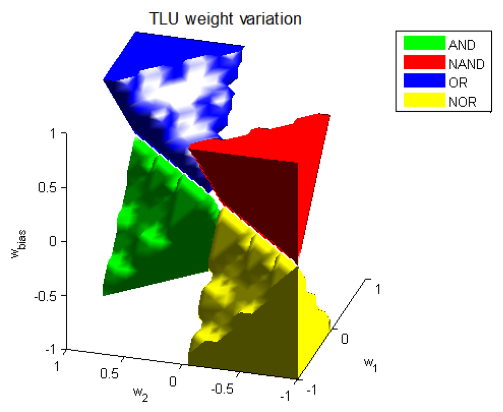
Figure 2.
Weight values necessary to realize the logic operations AND, OR, NAND and NOR.

Table 1.
Weight values chosen for linearly separable logic operations.
| Logic operation | |||
|---|---|---|---|
| NAND | −0.5 | −0.7 | 0.5 |
| NOR | −0.5 | −0.7 | −0.5 |
| AND | 0.3 | 0.6 | −0.5 |
| OR | 0.3 | 0.6 | 0.5 |
3. Memristive Devices
The Ag–Ch memristive device acts as a programmable two-terminal resistor, which can be programmed to assume a range of continuous resistance states. The resistance of the memristive device is decreased (“program" operation) and increased (“erase" operation) by applying positive and negative voltage pulses, greater than the device threshold voltage, respectively. The memristive device acts as a linear resistor when it receives an input below the threshold voltage. This behavior makes memristive devices suitable for use in reconfigurable hardware.
In our early design exploration using memristive devices, we are implementing neuromorphic circuits using discrete hardware. However, the true potential of these devices will be realized in the second-phase of our research where a fully-integrated platform with memristive devices fabricated in the back-end-of-the-line (BEOL) of a CMOS process will form compact reconfigurable circuit blocks.
A Verilog-A model for the memristive device has been developed and used with CMOS circuits for simulation in Spectre [27]. A memristive device model, similar to [28], is used to emulate the characteristics of the Boise State memristive device reported in [4,5,6,7,8,9,10], with appropriate device parameters. The Boise State memristors have been widely referenced by other researchers in their work [28,29,30,31,32,33]. This memristive model has a threshold voltage of 150 mV, while the read pulse voltage for the actual memristive devices fabricated and packaged at Boise State University should not exceed 20 mV for repeatable operation. This threshold voltage will be increased to the desired range using a modified material stack in the device. In our simulations, the initial state of the devices can be set to the desired resistance value. However, the algorithms assume random initial states, and all subsequent resistance changes are made through the application of voltage pulses.
4. Circuit Realization
The TLG defined in Equation (1) can be realized in discrete hardware using a summing op-amp circuit with memristive devices implementing the weights (). The target logic function is then realized by re-programming the weights (i.e., resistance) of the memristive devices.
To achieve the needed negative weights, the resistors (or memristive devices) are supplemented so the current coming out of the op-amp has the opposite direction of the input, and its combination with the variable current from the memristive device can take on both positive and negative values, Figure 3. The two resistors, and , determine the gain of the circuit that sets the range of weights possible in the circuit realization. Adjusting the resistance of the memristive device between 1 kΩ and 100 kΩ moves the weights in this range. Table 2 shows a set of target resistances for the memristors if kΩ and kΩ.
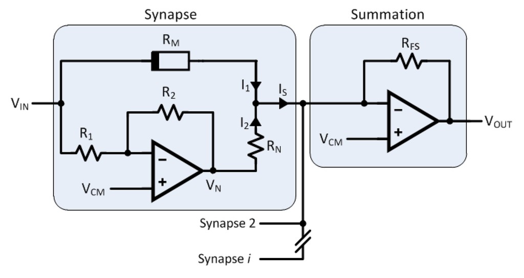
Figure 3.
Circuit implementation with memristive devices with circuitry for negative weights. In our circuit implementation the common mode voltage V.

Table 2.
Resistance values corresponding to theoretical weights in Table 1.
| Logic operation | |||
|---|---|---|---|
| NAND | 1.33 kΩ | 1.17 kΩ | 3.88 kΩ |
| NOR | 1.33 kΩ | 1.17 kΩ | 1.33 kΩ |
| AND | 2.81 kΩ | 4.81 kΩ | 1.33 kΩ |
| OR | 2.81 kΩ | 4.81 kΩ | 3.88 kΩ |
5. Memristive Device Characteristics
The memristive devices have been modeled in Cadence-Spectre and fabricated as physical devices. Programming the devices in both forms has the same basic approach. This approach and the necessary changes to that approach and observations about the physical devices are described next.
5.1. Simulations
The memristor model used in this paper is based on “A memristor device model" by C. Yakopcic [28] and is written in Verilog-A. The “state input" pin “” is used to sneak into the memristor state, but all memristor programming is done through the application of voltage pulses. The state input value is inversely proportional to the memristor resistance. A characterization of how the memristor state in the memristor model responds to the writing and erasing processes is shown in Figure 4. A series of positive and negative pulses with an amplitude of 200 mV were applied across the memristor. A pulse width of 1 μs was chosen so that the device is not under a constant stress. Applying a positive pulse causes the memristor to write, which decreases the memristor resistance, meaning that the “state" will be increasing. In contrast, applying a negative pulse causes the memristor to erase, which increases the memristor resistance, meaning that the “state" will be decreasing. Figure 5 shows the schematic of the programming circuit [34].
To read the current value of the memristor, the same circuit will be used, however, with a pulse amplitude that is much smaller than the threshold voltage. For the memristor model used in this paper, a (100 mV, 1 μs) pulse is chosen to be sufficiently small in order to avoid disturbing the current state of the device while reading it. The memristor resistance is then determined by measuring the output voltage of the circuit and applying Ohm’s law
The programming circuit in Figure 5 was built in Cadence first and then it was connected to Simulink using the Cadence coupler block. A MATLAB script was written to provide the voltage inputs to automatically drive the memristor to a desired resistance. The script generates programming pulses with amplitudes proportional to the difference between the current resistance of the memristor and the desired value . If the difference is large, it will send a bigger amplitude pulse and vice-versa. This amplitude gets smaller and smaller as the memristor approaches the desired resistance. The erasing process is more sensitive than the writing process; therefore, the gain in the erasing process is a factor of 1/3 smaller than the gain in the writing process. The programming pulse is limited below so that it will not destroy the device or cause clipping in the output voltage of this programming circuit.
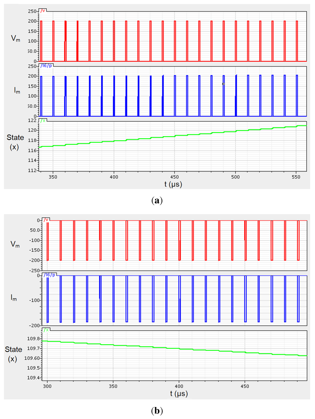
Figure 4.
Movement of the memristor state in response to the (a) writing and (b) erasing processes. Writing decreases the device resistance, while erasing increases the device resistance. The input pulses are shown in red (top window) and the current through the device is shown in blue (middle window). The third window shows the movement of the device state “x” ().
After each programming step, the MATLAB script will generate a reading pulse to read the current resistance of the device. In short, the programming circuit will keep sending pulses with an adapted amplitude to program, then read the memristor until its resistance is within a certain tolerance of the desired value. This behaves like a state machine in hardware. The operating range of the memristor in this paper is between 10 kΩ and 100 kΩ. The device was initialized at 40 kΩ, the desired value for the writing mode was 10 kΩ, and for the erasing mode was 100 kΩ. Figure 6 shows the amplitudes of the applied programming pulses and the measured memristor resistance after each programming cycle. The target resistance is highlighted in red. The script was able to drive the device to the desired resistance within a tolerance of 4 kΩ within an average of 10 programming cycles.
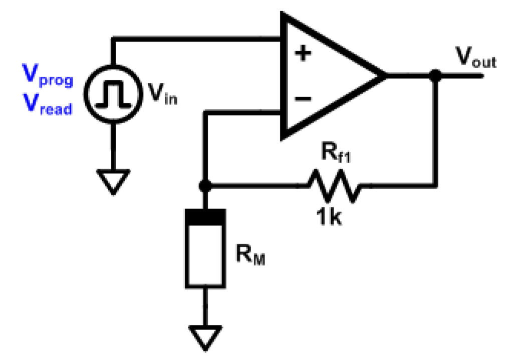
Figure 5.
Memristor programming circuit.
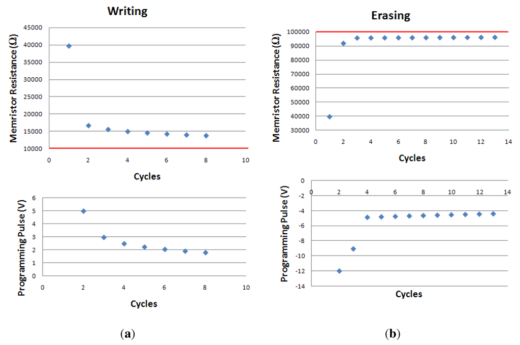
Figure 6.
Programming a single memristor. (a) Programming from 40 kΩ to 10 kΩ; (b) Programming from 40 kΩ to 100 kΩ.
5.2. Hardware
While our simulations used a non-idealized Verilog-A memristor model, when working with physical memristors the behavior of the devices is not fully predicted by the modeling equations. Experience with the characterization of these devices is employed to make circuits robust in the presence of these deviations from the simplistic understanding of memristive devices. The memristor model was designed as a curve fit to the data obtained from our physical memristors [28], but the full characteristics of the physical memristors are still being studied. Most studies are with a semiconductor parameter analyzer (SPA). Some experiments with physical memristors are shown here to understand how the memristors function in a circuit environment.
At this point there is no accurate model that foresees how much the memristor’s state will move if a voltage pulse of duration x and voltage y is applied. The writing and erasing voltages have to exceed a certain threshold for the memristor to change its state. The device has both a writing and an erasing threshold, which are not necessarily at the same absolute voltage level. Furthermore, these thresholds can change as the device’s resistance is altered, and the threshold of a device can change during its lifetime and was found to exhibit significant fluctuations between devices, making it even more difficult to make an accurate prediction of where the state is going to end up. It is therefore important to read the device’s state after each writing/erasing pulse so that programming error can be detected and compensated for by applying subsequent pulses. After programming the memristance can relax or drift, but certain programming pulses are less susceptible to the post-programming drift. For our application the amount of decay will not affect the final application response. For other applications that require finer memristance granularity, there would usually be a sequence of programming pulses and the subsequent pulses would “correct" any resulting drift. A typical writing/erasing algorithm will therefore need to send multiple pulses interspersed with reading pulses to the memristor.
Table 3 shows the threshold voltages that were found to work best for the devices under study. Note that these values are only valid for DC operation (slow pulses) and are not representative of the AC behavior of these devices. The following general rules have been developed to reach the desired state without damaging the memristor:
- -
- The reading voltage should be as low as possible to prevent unintentional ion movement. For the Ag–Ch devices used for this work, the reading voltage should not exceed 40 mV.
- -
- If a large reduction in resistance has been observed after applying a writing pulse, the device should be fully erased before applying another writing pulse. A large ΔR indicates hard device switching, meaning that most of the silver from the top electrode is embedded in the amorphous insulation layer. Applying another writing pulse might irreversibly damage the device.
- -
- Erasing pulses of very short duration and high enough amplitude can cause the device to go into negative differential resistance (NDR) mode or even damage the device. Repeated mild erase pulses will not cause long-term damage.

Table 3.
DC threshold levels for Ag–Ch memristors.
| Programming operation | Threshold (volts) |
|---|---|
| Writing | 0.23 V |
| Erasing | −0.58 V |
Figure 7 shows erasing and writing pulses applied to a silver-based device. The device is initially in low resistance state. Applying a low erasing pulse does not change its state, unless the erasing threshold is reached. At 15 ms, the device switches to a higher resistance because the erasing threshold listed in Table 3 is exceeded. The same is true for programming the device back to a lower resistance at 25 ms. The three programming pulses between 30 and 40 ms are bad examples as they violate one of the programming rules. If a larger ΔR is observed when writing, no more subsequent writing pulses should be applied as it could potentially harm the device. Note that the resistance in Figure 7 was only slightly reduced by the first pulse at 25 ms, indicating that the device has been sufficiently written. At 50 ms, the amplitude needed to erase the device is significantly higher than previously reported. This shows how the threshold levels can change while programming the device. The programming algorithm in this work was designed to accommodate these non-ideal characteristics.
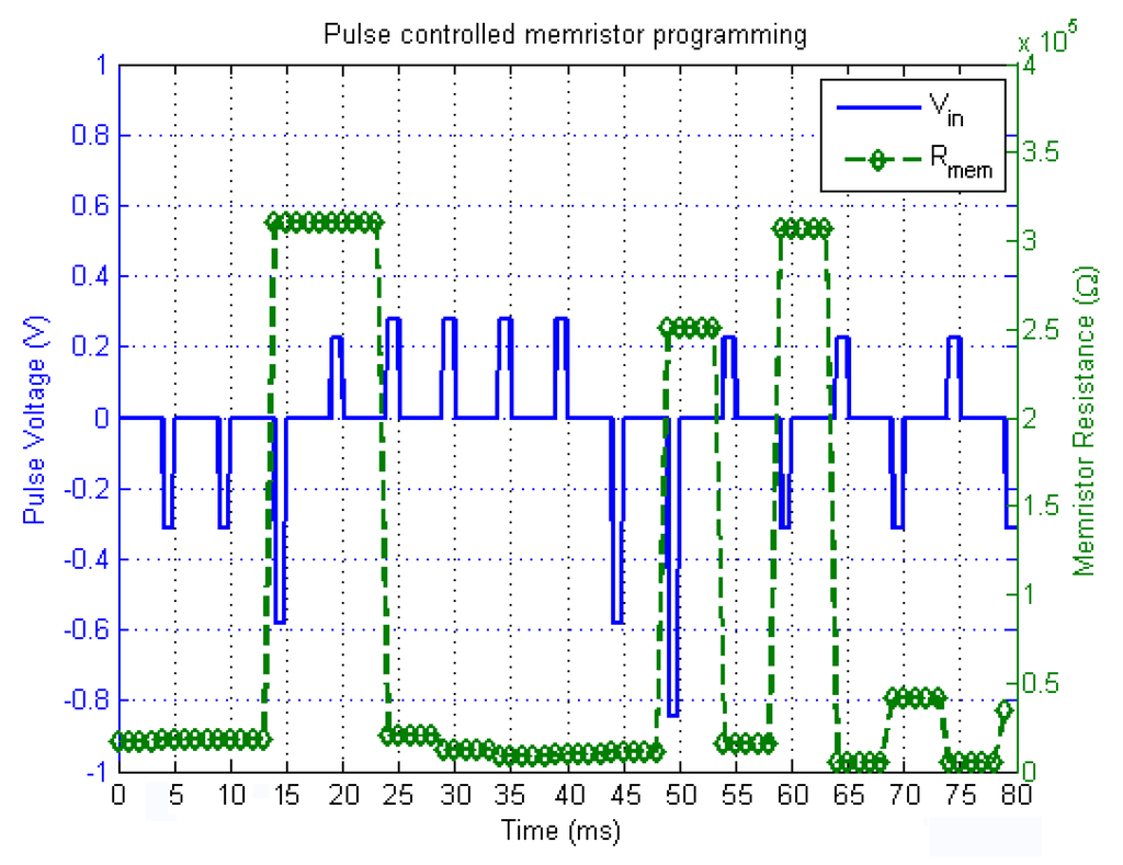
Figure 7.
Experimental response of the device to program and erase pulses. The program and erase threshold can be seen to move between pulses. The moving threshold can be observed by the change in memristance relative to the program and erase pulse heights.
The device used for this experiment performed well for several cycles, indicating that its integrity was not decreased. In fact, the “moving threshold” phenomenon was observed in all devices under study. The threshold levels listed in Table 3 were found to generally be accurate, but exhibited a deviation of up to 50% over a memristor’s lifetime. The moving threshold was observed because as every instance a voltage pulse is applied to change the resistance, there is an activation energy involved. At every step to move the Ag atoms to change the state, a higher pulse is required to affect the change. This gives the appearance of a moving threshold voltage. This variable threshold phenomenon has also been observed in other memristive devices [35].
In the Cadence memristor model a pulse train of writing pulses continues to decrease a memristor’s resistance, while an erasing pulse train continually increased its resistance, Figure 4. This is based on a simulation model, which does not have to follow the memristor programming rules as outlined above. The physical devices look moderately different compared with a simulated environment. Experiments on the devices confirmed this indication and it was found that continuously increasing or decreasing the resistance with fine control can be challenging to achieve in practice. This is especially true for continuous writing, as the programming rules prohibit us from continually sending writing pulses. It is therefore better to write the device and gradually erase it. In most cases, the devices would perform hard switching (i.e., jump from a low resistance to a high resistance and vice-versa). We chose a programming pulse that was suited to our application to enable us to jump in a single programming pulse between a high and low resistance value. Figure 8 shows the result of applying a pulse train of writing and erasing pulses with pulse amplitudes that are only slightly above the silver threshold levels (see Table 3) to a silver device. As can be seen, the resistance jumps up and down by at least two orders of magnitude in response to applied programming and erase pulses. The standard deviation was found to be around 45% for both high and low states. While this is a pretty significant variation, it enables the memristors to be used as a digital memory when toggling between the two states (high and low). The average high state resistance was found to be at 392 kΩ and the average low state resistance at 7.3 kΩ.
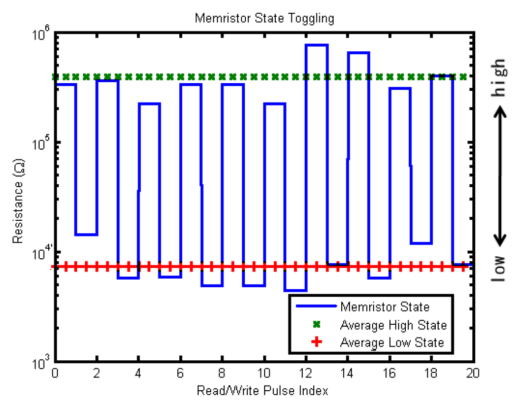
Figure 8.
Memristor characterization plot showing toggling between high and low memristance states.
Due to their intrinsic device structure and material characteristics, silver-based devices are expected to exhibit a certain hard-switching behavior, making them suitable to reprogrammable TLG use as the weights are polarized. It has been proposed that memristors would be suitable for use in ANNs, but these need finely variable resistances. Further device development and alternate circuitry and control methodologies may be necessary for these applications. The programmer used for this work is purely voltage controlled. While the presence of a threshold voltage suggests that the programmer should be voltage controlled, it is possible that the device should be programmed in current mode once the threshold voltage is reached. In fact, literature suggests that memristors are both a voltage and current controlled device [1,4], but no solutions are presented as to how a memristor is best controlled in a practical application such as an TLG or ANN programming circuit. The work in this paper starts to develop this.
Figure 8 shows the device has clear high and low states, but they vary significantly. It may seem as though the deviation of the values representing these high and low states is random and does not suggest that a relationship between previous state (resistance) and the change in resistance exists. However, when the change in resistance is analyzed numerically, a relationship between the change in resistance and the previous resistance is found to exist, but only when writing. Figure 9 shows data points from selected datasets that exhibited nice hard-switching behavior of the silver-based devices. When writing the devices to a lower resistance, the change in resistance is dependent on the previous state, but is independent of the pulse amplitude (the pulse amplitudes used here were all the same).
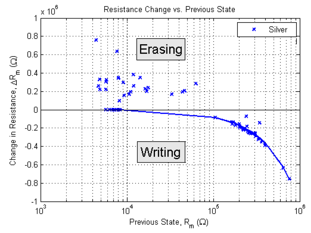
Figure 9.
Relationship between resistance change and previous state.
The resistance change can be said to be proportional to −1/R, where R is the resistance of the current state (before applying the pulse). This is consistent with literature investigating spike-timing-dependent-plasticity (STDP), which governs how synapses learn in biology [36]. This relationship between resistance change and previous state only holds for programming (i.e., reducing the resistance). When erasing, there seems to be no apparent pattern between the change and previous state. Given that the relationship is proportional to −1/R, it makes sense that this only applies when writing a memristor to a lower state, as the change in resistance will always be a negative number, indicating a reduction in resistance. Further, in Figure 8 it can be observed that with the selected program/erase voltage pulses, we could achieve a binary switch functionality desired for our 2-input Boolean logic application. For TLGs with a larger fan-in (), a more continuous range of weight values will be needed. A different scheme of adaptive program/erase voltage pulses would be applied to achieve the desired functionality.
6. Experiments and Results
The circuit described in Section 4 was created in a Cadence Simulation and also built as a physical circuit with discrete devices. In both cases the memristors were programmed to change the functionality of the TLG circuit alternately to AND, OR, NAND and NOR. Descriptions of these experiments and their results are described next.
6.1. Simulations
A feedback-based adaptive programming circuit was developed to program the individual memristive devices to predetermined resistance values to create each logic operation. The programming circuit in Figure 10 was built in Cadence and connected to Simulink using the Cadence coupler block. The memristor has to alternately be isolated for the circuit to apply the programming via the circuit in Figure 5 and be connected with the other memristors to the negative weight and summing circuitry in Figure 3. This is accomplished from switches shown in Figure 10.
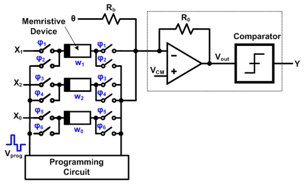
Figure 10.
Circuit implementation for programming memristive devices. In our circuit implementation the common mode voltage V.
A MATLAB-Simulink/Cadence co-simulation was run to realize four threshold logic gates: AND, OR, NAND, and NOR. The memristive devices were programmed by providing the voltage inputs through a charge-scaling DAC (digital to analog converter) with an iterative search process, using the device programming method described in Section 3 to automatically drive the memristor to reach the resistance values in Table 2 within a tolerance of 100 Ω. The program-and-erase operation is performed by applying positive and negative pulses (1 μs pulse width). After the memristive devices were programmed to match all the target resistances, a set of feed forward voltages was applied to the network to confirm the logic outputs for all four AND, OR, NAND, and NOR operations.
The results are shown in Figure 11. The waveform in the top frame of the plots shows the clock signal of the circuit, and the second and third frames show the two binary input signals. The amplitudes of these inputs are set within a range of 100 mV to not disturb the current state of the memristive device. The fourth waveform shows the output voltage superimposed on the 2.5 V virtual ground. The logic output of the comparator is displayed in the fifth window. The results show that the circuit built with memristive devices can be programmed and re-programmed to create the four desired logic operators. It is confirmed that the circuit design and programming procedure work correctly.
Simulations are often based on ideal behavior of devices. The MATLAB-Simulink/Cadence co-simulation tried to account for hardware-related phenomena as much as possible, and used the most realistic memristor model available, but there are still a lot of things that a simulation cannot account for. Dynamic range, noise and signal integrity are only a few examples. In order to build the simulated TLG entirely in hardware, a new programming circuit was developed to program and read the memristor devices.
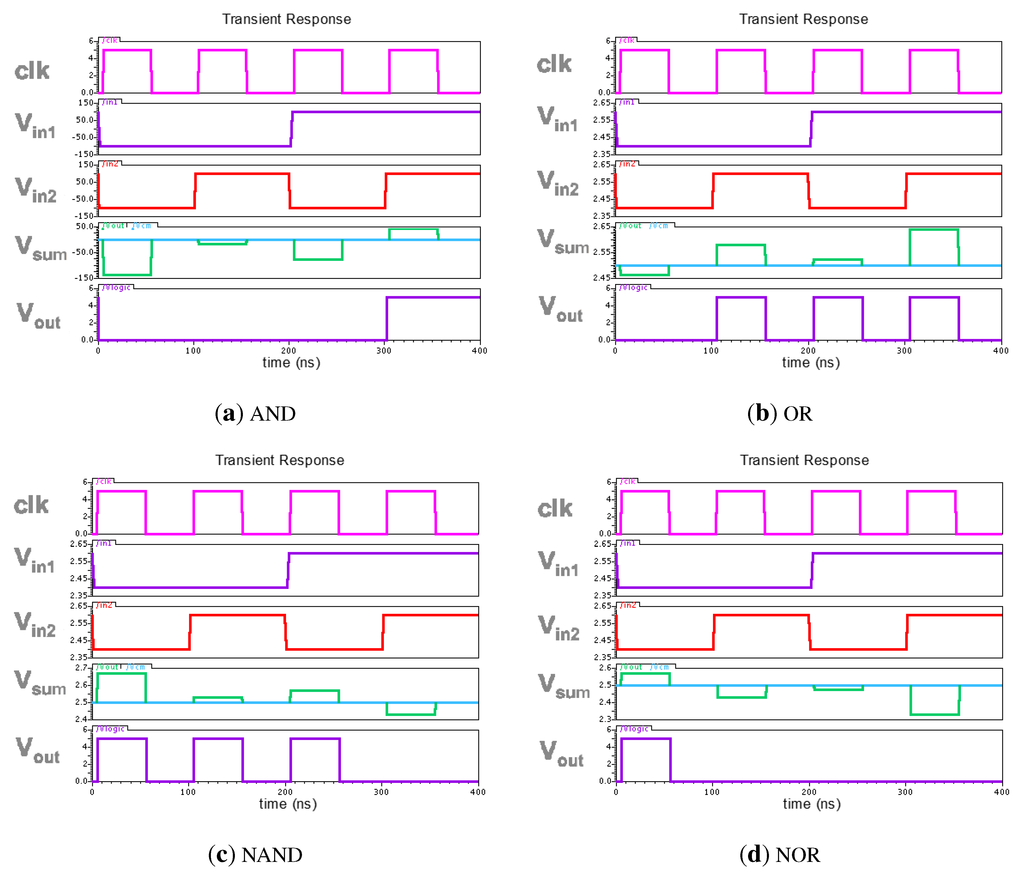
Figure 11.
Results of TLG circuit when programmed to each of the four logic operations. (a) AND; (b) OR; (c) NAND; (d) NOR. The output is valid only when the clock is high.
The programming setup used in the simulation is based on an op-amp in non-inverting configuration. The MATLAB-Simulink programming algorithm sends a pulse width and a pulse amplitude value to the Cadence simulation, which applies the programming pulse to the op-amp. The basic programming circuit used is shown in Figure 5. While this works fine in simulation, to build this circuit in hardware an op-amp supporting high speeds, high gains, and a wide dynamic range is needed and is hard to find. Given a fixed feedback resistor , the resistance value of the memristor can easily be determined by applying a pulse with a known pulse height to the positive input of the op-amp. The output is then a function of . However, depending on the value of , the gain of the op-amp can range from very small values to very large values. This dynamic range issue is not a big deal for simulations, but it is for hardware-based applications. In order to improve the dynamic range, the op-amp in Figure 5 is turned into a programmable gain amplifier (PGA) by adding different feedback resistors in parallel to the existing feedback resistor . These additional resistors can be connected with switches to change the effective feedback resistance and therefore the gain of the PGA, Figure 12.
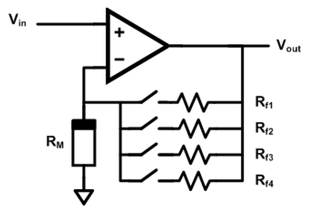
Figure 12.
Programmable gain amplifier used to program memristors.
The output of the PGA for different memristor resistance values is shown in Figure 13. Note that there are four feedback resistors in Figure 12, but Figure 13 only shows three curves. This is because the first of the four resistors () is only used for programming and not reading on the memristor device. We limited our circuit to a range from 1 kΩ to 200 kΩ such that when programming, the gain of the PGA is set sufficiently small. With a 1 kΩ feedback resistance, the programming current is also sufficiently limited such that the device will not be destroyed when its resistance is drastically reduced.
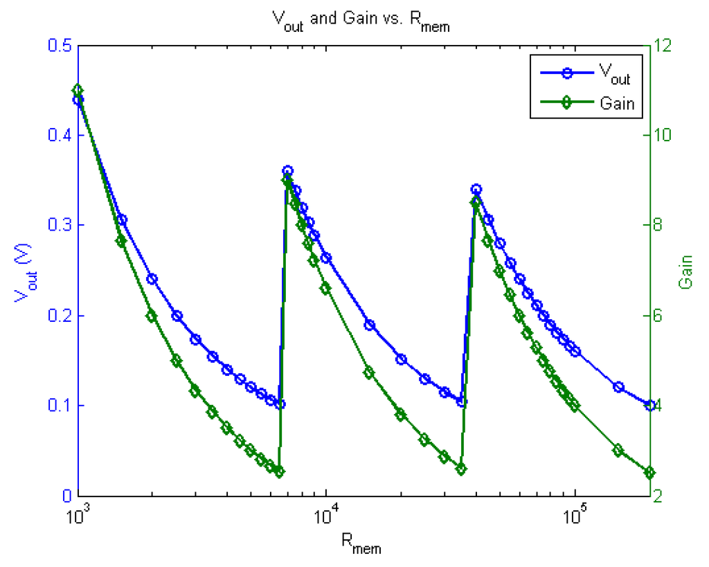
Figure 13.
Output of programming/reading circuit with programmable gain.
An FPGA (field programmable gate array) and a high-speed DSP (digital signal processing) board are used to generate the programming pulses and to read the response () of the programming circuit. A host computer communicates with a Nios-II soft-core processor implemented on the FPGA, controlling the pulse generation module also implemented on the FPGA. The pulse generation module generates both programming and reading pulses through a high-speed DAC, controls the switches for the PGA and reads the response of the memristor using an ADC (analog to digital converter). When reading a memristive device, a small reading pulse (20–40 mV) is applied and the response of the PGA is read back by the DSP board’s DAC and is further processed by the FPGA. For the Ag–Ch devices, a pulse with fixed pulse width of 10 μs and variable amplitude was used.
For the simulation where greater control of the memristor is possible, exact target resistances were calculated in Table 1. Since the zones of acceptable weight values are large, binary toggling of the device was utilized for the hardware implementation. The weight values in Table 1 are therefore quantized to produce the binary states in Table 4. These correspond to the four corners of the weight cube in Figure 2 where a logic operation of interest is located.

Table 4.
Binary memristor states for each logic function.
| Logic operation | |||
|---|---|---|---|
| AND | high kΩ | high kΩ | low kΩ |
| OR | high kΩ | high kΩ | high kΩ |
| NAND | low kΩ | low kΩ | high kΩ |
| NOR | low kΩ | low kΩ | low kΩ |
Figure 10 shows the fully connected TLG with quantizer (activation function of the neuron) and programming circuit attached. The switches are needed to disconnect each memristor individually and connect it to the programmer for reconfiguration. This circuit was built from discrete components. Memristors were packaged and connected. The circuit board is shown in Figure 14.
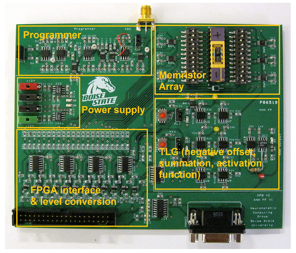
Figure 14.
TLG programming circuit.
The performance of the TLG was measured by the four basic logic operations (AND, OR, NAND, NOR), but there are a total of 16 two-input logic operations possible, 14 of which could be achieved by this circuit. The remaining 12 cases for the purposes of this paper are described as invalid or “other" logic operations. In Figure 15 the output of the TLG through several cycles of programming to take on different logic operations is shown. The top two frames show the input signals cycling through 4 input options, then resting while voltages are applied to change the memristor’s state. The resulting output signals after each reprogramming cycle are shown in frame 3. Frames 4 and 5 show additional results that were generated after the first set of results. They use the same functional inputs as frames 1 and 2. This clearly shows that the TLG can be reconfigured to many more possible functions. Since we used memristors, it is non-volatile and retains the settings even when we remove the power source.
The programming intervals in Figure 15 indicate where a single memristor was programmed according to Table 4. As Table 4 shows, going from an AND to a NOR configuration requires two memristors to change (memristor 1 and 2 need to change from high to low; memristor 3 stays low). Therefore, it required two programming cycles—one for each memristor—to reconfigure the TLG. In order to reconfigure the TLG from an AND to an OR or a NAND to a NOR configuration, only one programming cycle is required, as the bias weight (memristor 3) is the only one that needs to be changed.
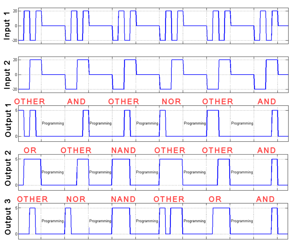
Figure 15.
TLG inputs and outputs.
Figure 16a shows the weight space with a possible programming path for reconfiguring the TLG from NOR to OR. In this case it will take a total of three programming cycles as all three memristors need to be changed. As Figure 16a shows, the path from NAND to OR leads through a corner that is not one of the four functions used for this work. Figure 16b shows the programming paths required to obtain all the results in Figure 15 in the order presented. As can be seen, the TLG is reconfigured to operate only in the corner regions. Four of the eight corners are valid configurations (AND, OR, NAND, NOR), while the rest are unused configurations and are simply used as way-points to reconfigure the TLG from one function to another.
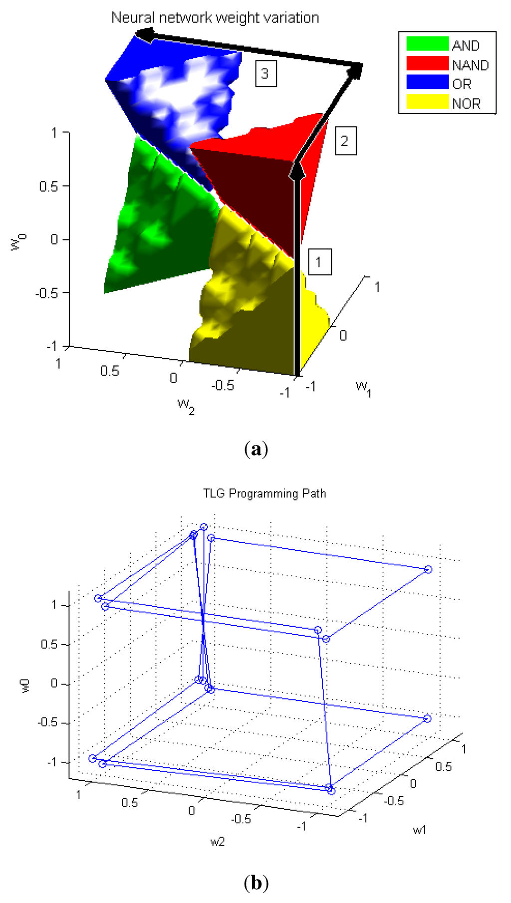
Figure 16.
(a) Weight cube indicating the programming path required to go from NOR to OR and (b) all programming paths required to obtain the results seen in Figure 15.
7. Conclusions
We have developed a circuit design capable of realizing four different logic operations by changing the resistance of the memristive devices. The resistance is changed through an iterative procedure through the application of voltage pulses to reach resistances determined outside the circuit. This was implemented first in simulation, and this same circuit with only minor modifications was then physically realized on a printed circuit board (PCB). The memristors in this circuit were reprogrammed based on voltage pulses determined by an FPGA so the circuit could take on the four logic operations of interest.
We believe that this is the first reported experimental demonstration of a reprogrammable TLG circuit with physical memristors. This work developed a greater understanding of the constraints involved when using memristors in complete circuits, instead of in signal analyzers. Techniques necessary to work with these memristors were also developed.
This programming procedure can be replaced by a learning algorithm, such as back propagation, to determine the resistance values based on input-output pairs. Memristors and a control circuitry that can attain finer granularity in resistances will be needed. The switching circuitry introduced a high level of overhead. Future work should look at alternate approaches to do both programming and use of the memristors without this.
The prototype TLG circuit, presented in this paper, used discrete circuit components to demonstrate the hybrid memristor and circuit application. Due to the limitations set by the available discrete op-amps, a 5 V supply was used. Eventually, the memristive devices will be fabricated in the back-end-of-the-line (BEOL) on a CMOS chip, with a compact TLG circuit implementation and comprised of the peripheral circuits for program and read operations. A lower supply voltage and smaller device geometries in nanometer CMOS processes would result in significant power savings. Further, the integrated version of the threshold logic gate would use a compact transistor level implementation instead of a power hungry op-amp. Our work thus far has explored feasibility of two-input TLGs with Ag–Ch memristive devices. In the future, hybrid CMOS-memristor integrated TLGs are expected to have fan-in of >10, switching speed >1 GHz and dissipate lower static power than a corresponding pure-CMOS logic implementation. Such high density of integration will allow development of several new applications.
Acknowledgments
The authors gratefully acknowledge Kolton Drake and Stephen Stauts for invaluable support with testing and packaging of memristors and Jeanette Brooks for assistance with PCB assembly.
References
- Strukov, D.B.; Snider, G.S.; Stewart, D.R.; Williams, R.S. The missing memristor found. Nature 2008, 453, 80–83. [Google Scholar] [PubMed]
- Strukov, D.B.; Likharev, K.K. A Reconfigurable Architecture for Hybrid CMOS/Nanodevice Circuits. In Proceedings of the 14th ACM/SIGDA International Symposium on Field Programmable Gate Arrays, Monterey, CA, USA, 22–24 February 2006; pp. 131–140.
- Beiu, V.; Quintana, J.M.; Avedillo, M.J. VLSI implementations of threshold logic—A comprehensive survey. IEEE Trans. Neural Netw. 2003, 14, 1217–1243. [Google Scholar] [CrossRef] [PubMed]
- Oblea, A.S.; Timilsina, A.; Moore, D.; Campbell, K.A. Silver Chalcogenide Based Memristor Devices. In Proceedings of the International Joint Conference on Neural Networks (IJCNN), Barcelona, Spain, 18–23 July 2010; pp. 1–3.
- Campbell, K.A. Variable integrated analog resistor. U.S. Patent No. 8238146, August 2012. [Google Scholar]
- Campbell, K.A. SnSe-based limited reprogrammable cell. U.S. Patent No. 8101936, January 2012. [Google Scholar]
- Campbell, K.A.; Moore, J.T. Silver-selenide/chalcogenide glass stack for resistance variable memory. U.S. Patent No. 8080816, December 2011. [Google Scholar]
- Campbell, K.A. Resistance variable memory device and method of fabrication. U.S. Patent No. 7868310, January 2011. [Google Scholar]
- Campbell, K.A. Differential negative resistance memory. U.S. Patent No. 7745808, June 2010. [Google Scholar]
- Campbell, K.A.; Moore, J.T. Silver-selenide/chalcogenide glass stack for resistance variable memory. U.S. Patent No. 7646007, January 2010. [Google Scholar]
- Tran, T.; Rothenbuhler, A.; Barney Smith, E.H.; Saxena, V.; Campbell, K.A. Reconfigurable Threshold Logic Gates Using Memristive Devices. In Proceedings of the IEEE Subthreshold Microelectronics Conference, Waltham, MA, USA, 9–10 October 2012.
- Merrikh-Bayat, F.; Shouraki, S.B. Memristor-based circuits for performing basic arithmetic operations. Procedia Comput. Sci. 2011, 3, 128–132. [Google Scholar] [CrossRef]
- Di Ventra, M.; Pershin, Y.V.; Chua, L.O. Circuit elements with memory: Memristors, memcapacitors, and meminductors. Proc. IEEE 2009, 97, 1717–1724. [Google Scholar] [CrossRef]
- Yuriy, P.V.; Di Ventra, M. Practical approach to programmable analog circuits with memristors. IEEE Trans. Circuits Syst. Regul. Pap. 2010, 57, 1857–1864. [Google Scholar]
- Talukdar, A.; Radwan, A.G.; Salama, K.N. Generalized model for Memristor-based Wien family oscillators. Microelectron. J. 2011, 42, 1032–1038. [Google Scholar] [CrossRef]
- Muthuswamy, B. Implementing memristor based chaotic circuits. Int. J. Bifurc. Chaos 2010, 20, 1335–1350. [Google Scholar] [CrossRef]
- Rose, G.S.; Rajendran, J.; Manem, H.; Karri, R.; Pino, R.E. Leveraging memristive systems in the construction of digital logic circuits. Proc. IEEE 2012, 100, 2033–2049. [Google Scholar] [CrossRef]
- Victor, E.; Howard, G.D.; Adamatzky, A. Organic memristor devices for logic elements with memory international. J. Bifurc. Chaos 2012, 22, 1250283. [Google Scholar] [CrossRef]
- Qiangfei, X.; Robinett, W.; Cumbie, M.W.; Banerjee, N.; Cardinali, T.J.; Yang, J.J.; Wu, W.; Li, X.; Tong, W.M.; Strukov, D.B.; Snider, G.S.; Medeiros-Ribeiro, G.; Williams, R.S. Memristor? CMOS hybrid integrated circuits for reconfigurable logic. Nano Lett. 2009, 9, 3640–3645. [Google Scholar]
- Robinett, W.; Pickett, M.; Borghetti, J.; Qiangfei, X.; Snider, G.S.; Medeiros-Ribeiro, G.; Williams, R.S. A memristor-based nonvolatile latch circuit. Nanotechnology 2010, 21. [Google Scholar] [CrossRef] [PubMed]
- Snider, G.S. Self-organized computation with unreliable, memristive nanodevices. Nanotechnology 2007, 18, 1–13. [Google Scholar] [CrossRef]
- Adhikari, S.P.; Yang, C.; Kim, H.; Chua, L.O. Memristor bridge synapse-based neural network and its learning. IEEE Trans. Neural Netw. Learn. Syst. 2012, 23, 1426–1435. [Google Scholar] [CrossRef] [PubMed]
- Ziegler, M.; Soni, R.; Patelczyk, T.; Ignatov, M.; Bartsch, T.; Meuffels, P.; Kohlstedt, H. An electronic version of Pavlov’s dog. Adv. Funct. Mater. 2012, 22, 2744–2749. [Google Scholar] [CrossRef]
- Bichler, O.; Zhao, W.; Alibart, F.; Pleutin, S.; Lenfant, S.; Vuillaume, D.; Gamrat, C. Pavlov’s dog associative learning demonstrated on synaptic-like organic transistors. Neural Comput. 2013, 25, 549–566. [Google Scholar] [CrossRef] [PubMed]
- Yu, S.; Wu, Y.; Jeyasingh, R.; Kuzum, D.; Wong, H.-S.P. An electronic synapse device based on metal oxide resistive switching memory for neuromorphic computation. IEEE Trans. Electron Devices 2011, 58, 2729–2737. [Google Scholar] [CrossRef]
- Jo, S.H.; Chang, T.; Ebong, I.; Bhadviya, B.B.; Mazumder, P.; Lu, W. Nanoscale memristor device as synapse in neuromorphic systems. Nano Lett. 2010, 10, 1297–1301. [Google Scholar] [CrossRef] [PubMed]
- Pino, R.; Bohl, J.W.; McDonald, N.; Wysocki, B.; Rozwood, P.; Campbell, K.A.; Oblea, A.; Timilsina, A. Compact Method for Modeling and Simulation of Memristor Devices: Ion Conductor Chalcogenide Based Memristor Devices. In Proceedings of the 2010 IEEE/ACM International Symposium on Nanoscale Architectures (NANOARCH), Anaheim, CA, USA, 17–18 June 2010; pp. 1–4.
- Yakopcic, C.; Taha, T.M.; Subramanyam, G.; Pino, R.E.; Rogers, S. A memristor device model. IEEE Electron Device 2011, 32, 1436–1438. [Google Scholar] [CrossRef]
- Yakopcic, C.; Taha, T.M.; Subramanyam, G.; Shin, E.; Murray, P.T.; Rogers, S. Memristor-basedPattern Recognition for Image Processing: An Adaptive Coded Aperture Imaging and Sensing Opportunity. In Proceedings of the Adaptive Coded Aperture Imaging, Non-Imaging, and Unconventional Imaging Sensor Systems II, San Diego, CA, USA, 1 August 2010; Volume 7818, p. 78180E.
- Yakopcic, C.; Sarangan, A.; Gao, J.; Taha, T.M.; Subramanyam, G.; Rogers, S. TiO2 Memristor Devices. In Proceedings of the 2011 IEEE National Aerospace and Electronics Conference (NAECON), Dayton, OH, USA, 20–22 July 2011; pp. 101–104.
- Yakopcic, C.; Taha, T.M.; Subramanyam, G.; Pino, R.E.; Rogers, S. Analysis of a Memristor Based 1T1M Crossbar Architecture. In Proceedings of the 2011 International Joint Conference on Neural Networks (IJCNN), San Jose, CA, USA, 31 July–5 August 2011; pp. 3243–3247.
- Yakopcic, C.; Taha, T.M.; Subramanyam, G.; Rogers, S. Memristor-based unit cell for a detector readout circuit. SPIE Optical Eng. Appl. 2011, 8165, 81651F. [Google Scholar]
- Yakopcic, C.; Taha, T.M.; Subramanyam, G.; Pino, R.E. Memristor SPICE modeling. In Advances in Neuromorphic Memristor Science and Applications; Springer: Berlin, Germany, 2012; pp. 212–244. [Google Scholar]
- Drake, K.; Campbell, K.A. Chalcogenide-Based Memristive Device Control of a Lego Mindstorms NXT Servo Motor. In Proceedings of the AIAA Infotech at Aerospace Conference and Exhibit, St. Louis, MO, USA, 29–31 March 2011.
- Jo, S.H.; Kim, K.-H.; Lu, W. Programmable resistance switching in nanoscale two-terminal devices. Nano Lett. 2008, 9, 496–500. [Google Scholar] [CrossRef] [PubMed]
- Zamarreño-Ramos, C.; Camuñas-Mesa, L.A.; Pérez-Carrasco, J.A.; Masquelier, T.; Serrano-Gotarredona, T.; Linares-Barranco, B. On spike-timing-dependent-plasticity, memristive devices, and building a self-learning visual cortex. Front. Neurosci. 2011, 5(26). [Google Scholar] [CrossRef] [PubMed]
© 2013 by the authors; licensee MDPI, Basel, Switzerland. This article is an open access article distributed under the terms and conditions of the Creative Commons Attribution license (http://creativecommons.org/licenses/by/3.0/).