1. Introduction
Since the 1990s, various families of fully-depleted SOI MOSFET have been proposed and extensively studied [
1,
2] due to their various merits in terms of device scaling (high drivability, steep swing, less short-channel effects, smaller foot print,
etc.). One of the authors (Omura) proposed the cross-current tetrode SOI MOSFET (XCT-SOI MOSFET) for analog applications (see
Figure 1), in 1986, on the basis of partially-depleted SOI MOSFET technology [
3], and conducted experiments to evaluate the fundamental aspects of the device. While the scaling feasibility of XCT-like devices has been studied recently [
4,
5], we expect that XCT-SOI devices will yield new applications, such as medical implants, which demand low-energy operation with high noise margin. In order to discuss those applications in detail, device models have already been proposed to perform circuit simulations [
6,
7]. However, modeling an XCT-SOI device is not so easy due to the three-dimensionality of its operations [
3,
5]. Recently, our laboratory group examined the device model proposed in [
6], and its usefulness was comprehensively revealed [
8]. In addition, a mechanism analysis demonstrated the potential of scaled XCT CMOS devices for extremely-low-energy operation [
9].
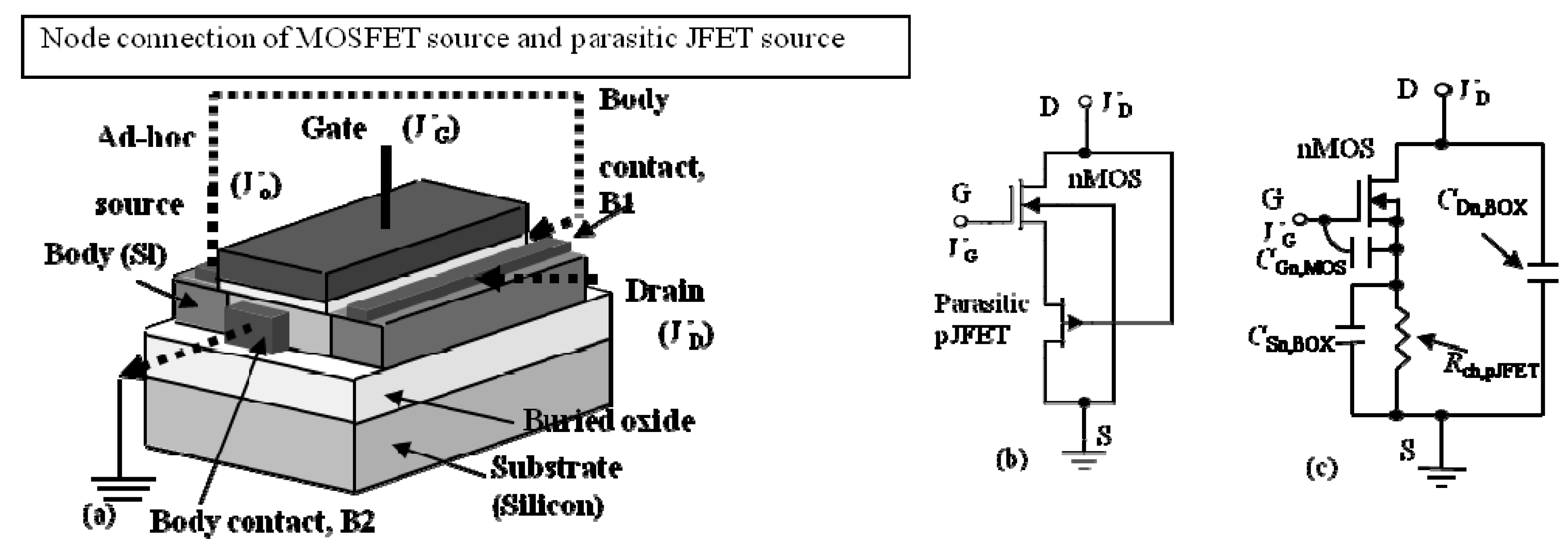
Figure 1.
XCT-SOI MOSFET (bird’s eye view and equivalent circuit models): (
a) Bird’s eye view of XCT-SOI device with parameter definitions and current flow. Broken arrows reveal the current flow; (
b) Basic equivalent circuit model of n-XCT-SOI MOSFET [
3]; and (
c) AC circuit model of n-XCT-SOI MOSFET [
9].
This paper considers the dynamic and standby power dissipation characteristics of the sub-30-nm-long gate XCT-SOI MOSFET. We start by analyzing the low-energy operation of XCT-SOI CMOS circuits; the model proposed here strongly suggests that the “source potential floating effect (SPFE)” substantially reduces the operation power consumption. The great advantages of the design methodology are also elucidated. In addition, this study addresses the reality of sub-20-nm-long gate XCT-SOI devices and a scaling scheme to suppress the standby power consumption for future low-energy applications.
3. Circuit Simulation Results of SOI CMOS and XCT-SOI CMOS
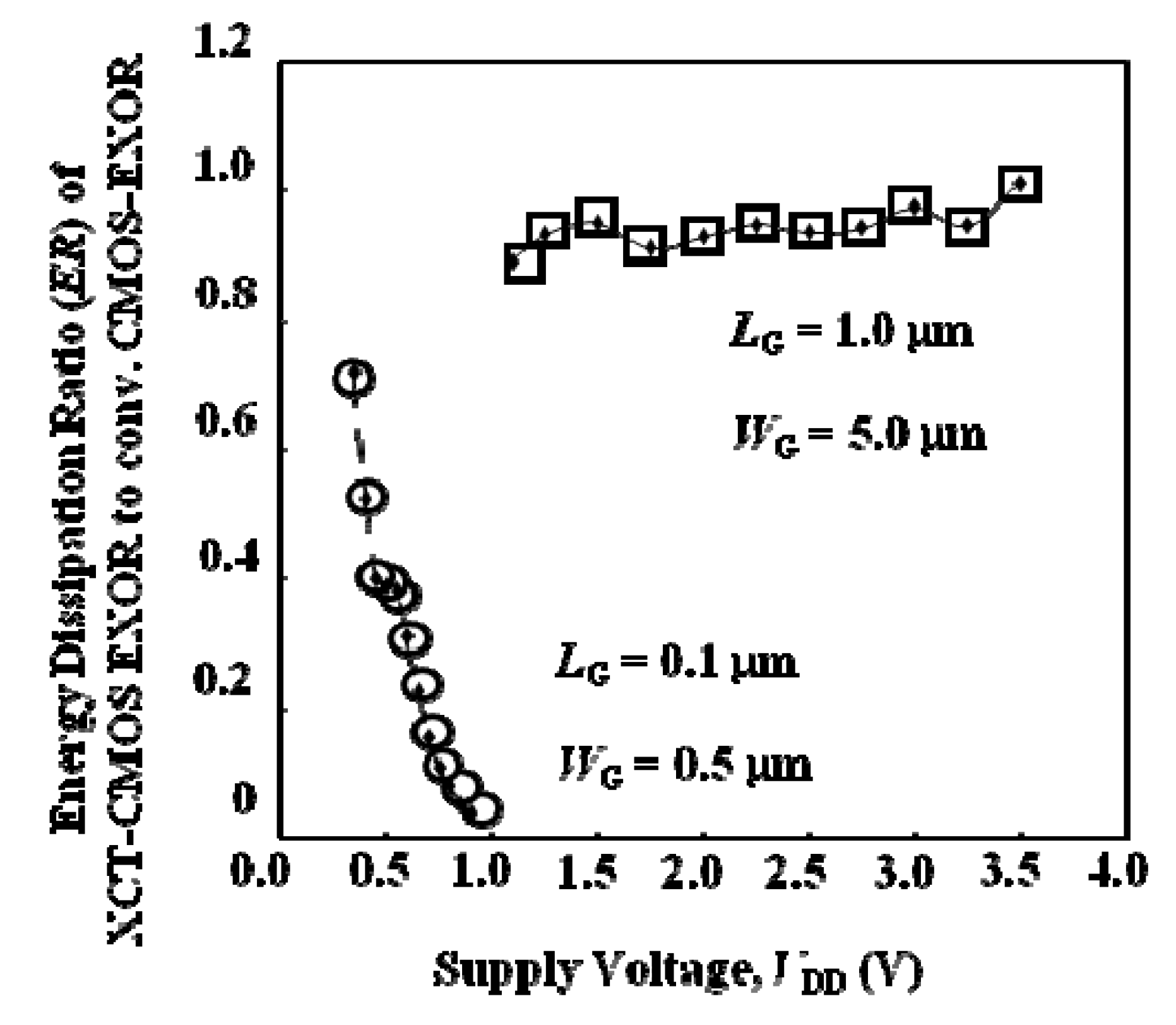
Here, we advance the discussion to better understand XCT-CMOS EXOR circuit features. We assume the OR-NAND type EXOR circuit that consists of four CMOS inverters (standard layout). We concentrate the discussion on the energy ratio of CMOS-EXOR circuits, where energy ratio (
ER) is defined as the energy dissipated by the XCT-CMOS EXOR over that of the comparable conventional SOI-CMOS EXOR. Calculation results, based on HSPICE [
11] simulation results, are shown in
Figure 3.
Figure 3.
Simulation results of energy ratio (ER) of the energy dissipation of 1.0-μm-long gate CMOS EXOR and 100-nm-long gate CMOS EXOR. The energy ratio is defined by the energy dissipated by the XCT-EXOR divided by that of the conventional CMOS EXOR.
Figure 3.
Simulation results of energy ratio (ER) of the energy dissipation of 1.0-μm-long gate CMOS EXOR and 100-nm-long gate CMOS EXOR. The energy ratio is defined by the energy dissipated by the XCT-EXOR divided by that of the conventional CMOS EXOR.
First, it is seen that the ER value of 1-μm-long gate devices is almost unity regardless of the VDD value. This behavior is reasonable for the following reasons. The energy dissipation of conventional devices, evaluated by the Pd-td product, is not a function of VDD due to the simple recognition of the MOS gate capacitor’s charging and discharging operations. It is anticipated that the XCT-CMOS, with a 1-μm-long gate, follows this principle. In the case of 0.1-μm-long gate devices, on the other hand, it is seen that the ER value rapidly falls as VDD rises. As this is a very interesting result and somewhat mysterious, we discuss below a possible mechanism based on physics.
Frequency-dependent energy ratio (
ER) is defined by [
9]:
where
CGn,XCT and
CGp,XCT denote the effective gate capacitance of
n-XCT-SOI MOSFET and
p-XCT-SOI MOSFET, respectively. Here, for simplicity, we do not take account of the depletion layer beneath the buried oxide layer. These capacitances are calculated using the equivalent circuit model shown in
Figure 1c as:
At the low-frequency limit (ω→0),
CGn,XCT and
CGp,XCT are reduced to
CGn,MOS and
CGp,MOS, respectively, as expected. At the high-frequency limit, however, we have:
Generally speaking, reducing the gate length (
LG) raises the operation frequency at the same supply voltage. The
ER rises when the scaling is enhanced; the scaling scheme assumed here [
5,
8] slightly reduces
CSn,BOXRch,pJFET and
CSp,BOXRch,nJFET as the scaling is advanced. For
f < 1/(
CSn,BOXRch,pJFET) and
f < 1/(
CSp,BOXRch,nJFET), the roles of
CSn,BOX and
CSp,BOX are lost;
i.e., we have
CGn,XCT~ CGn,MOS and
CGp,XCT~ CGp,MOS. This is equivalent to the low-frequency limit. As a result, the
ER value approaches unity; the intrinsic advantage of the XCT-SOI CMOS is lost. For
f > 1/(
CSn,BOXRch,pJFET) and
f > 1/(
CSp,BOXRch,nJFET), on the other hand, we have
CGn,XCT < CGn,MOS and
CGp,XCT < CGp,MOS. Device operation approaches the high-frequency limit. In this case, the
ER value decreases as the frequency rises. The
ER value approaches zero as the supply voltage rises, shown in
Figure 3. It is anticipated that the depletion layer beneath the buried oxide layer reduces the parasitic capacitance of source diffusion. In order to achieve a small
ER value, therefore, we have to increase the effective channel resistance of the parasitic JFET when scaling is advanced.
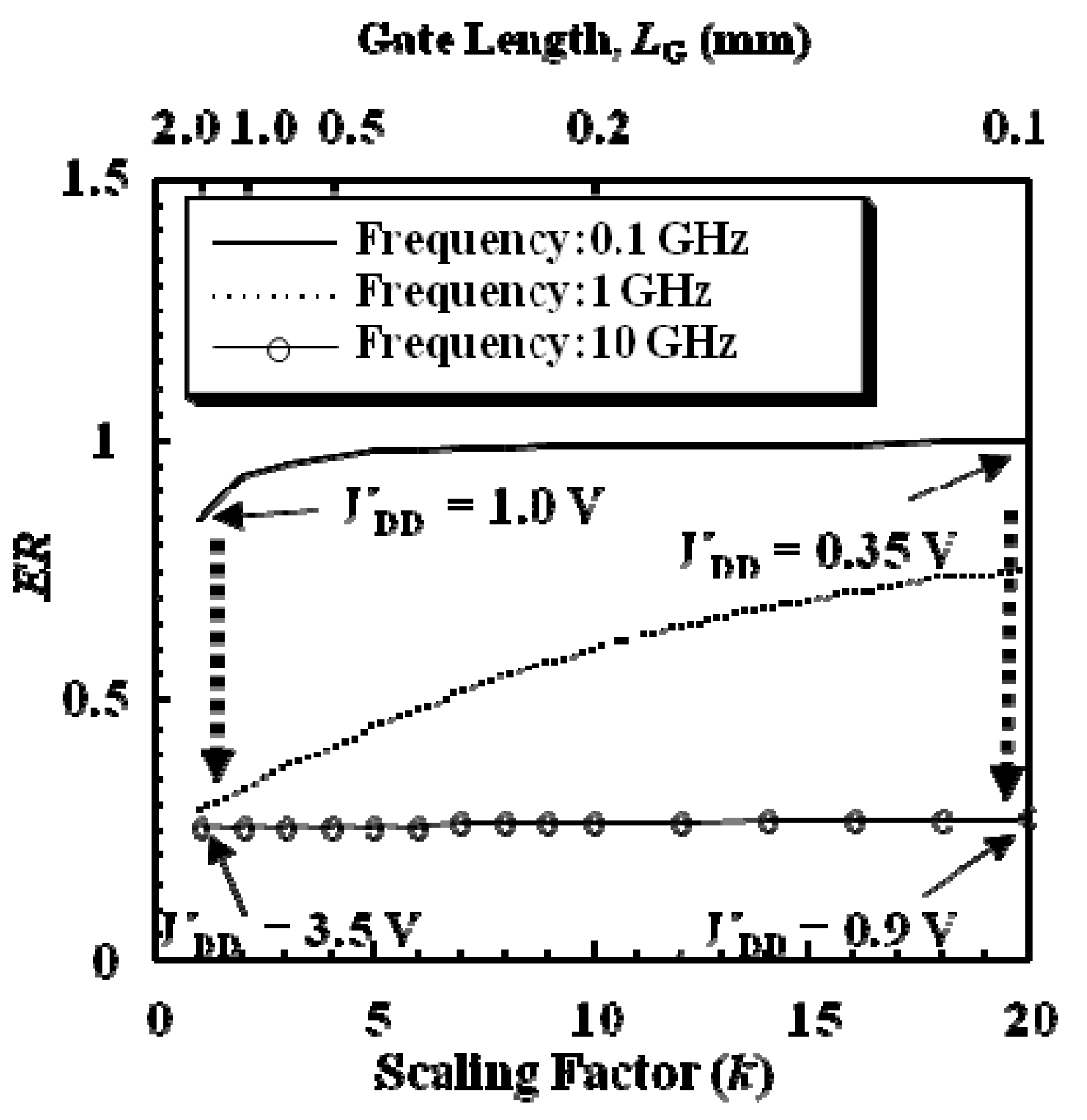
Calculation results of the energy ratio (
ER), defined by Equations (1) and (2), are shown in
Figure 4. The model clearly predicts that high-frequency drive will drastically reduce XCT-SOI CMOS power consumption. This stems from the “
source potential floating effect (SPFE)” obtained by the model shown in
Figure 1c. Consequently, we can conclude that the SPFE of the source diffusion of the SOI MOSFET plays an important role in reducing the energy dissipated by XCT-SOI CMOS devices.
Figure 4.
Dissipated energy ratio as a function of the scaling factor. It is assumed that the energy dissipation consists only of the charging and discharging processes of the gate capacitor. Scaling scheme is described in [
5]. The dotted arrows reveal the lowest-to-highest range of supply voltage applicable to 1-μm-long gate CMOS (for
k = 1) and 0.1-μm-long gate CMOS (
k = 20).
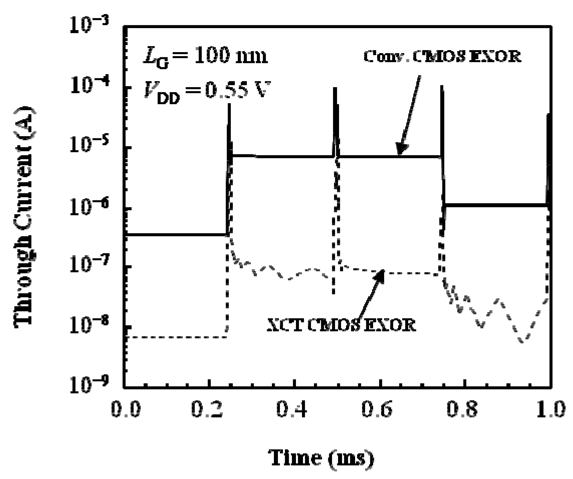
Figure 5 shows simulation results of the time-dependent through-current of the conventional SOI CMOS EXOR chain circuit and the XCT-SOI CMOS EXOR chain circuit, both under dynamic operation. It is seen that the standby power of the XCT-SOI CMOS EXOR chain circuit is about two orders lower than that of the conventional SOI CMOS EXOR chain circuit. This suggests that logic circuits composed of XCT-SOI CMOS can offer drastically lower standby-energy dissipation as well as lower switching-energy dissipation.
Figure 5.
Simulation results of through-current of CMOS EXOR for LG = 100 nm. Arrows show standby power reduction.
Figure 5.
Simulation results of through-current of CMOS EXOR for LG = 100 nm. Arrows show standby power reduction.
4. Further Scaling Potential of XCT-SOI MOSFET
We now investigate the scaling potential of the XCT-SOI CMOS. The fundamental scaling scheme of the XCT-SOI MOSFET has been already studied in [
5,
8] and a 100-nm-long gate XCT-SOI CMOS has been realized. However, body doping is apt to rise to 10
19 cm
−3 as the XCT-SOI MOSFET is inherently a partially-depleted SOI device. We investigated how well the XCT-SOI MOSFET can be scaled down to realize a 15-nm-long gate. Using 3D device simulations [
10], we simulated the performance of 20-nm-long gate and 15-nm-long gate XCT-SOI MOSFETs under the scaled bias condition, where we assumed abrupt source and drain junctions, for simplicity, in the scaling scheme proposed recently [
12]. As the previous scheme [
5,
8] cannot be applied to the sub-100-nm regime, we restructured the scheme (see
Table 1) so that devices work well [
12].
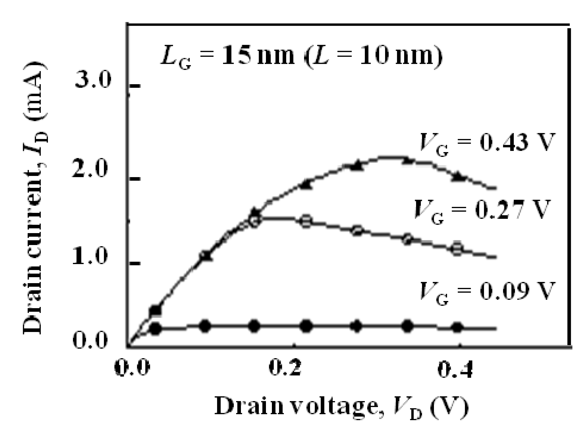
Here, simulated
ID-VD characteristics of the 15-nm-long gate XCT-SOI MOSFET, with device parameters, shown in
Table 1, shown in
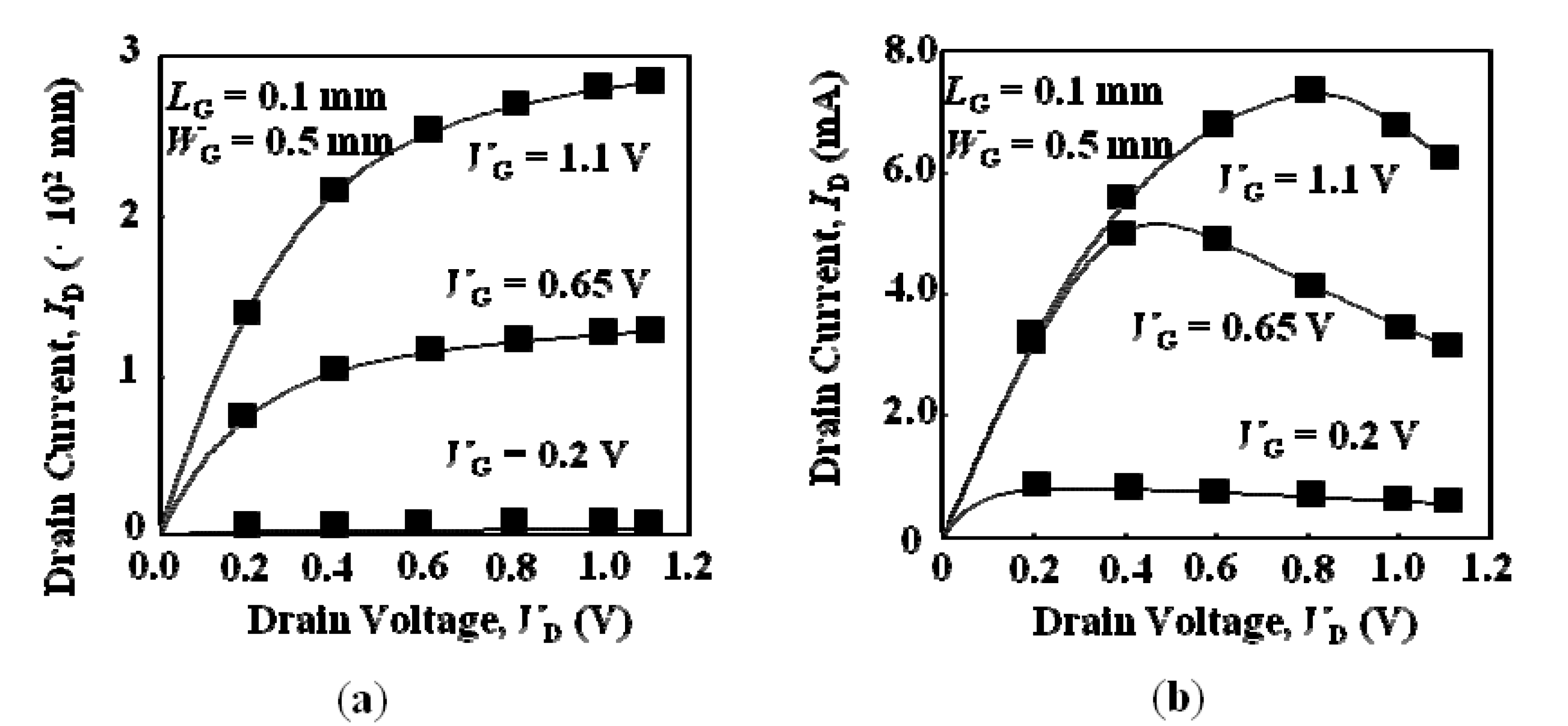
Figure 6; the device has the abrupt source and drain junctions. The device shows the negative differential conductance in the saturation region, as is expected.
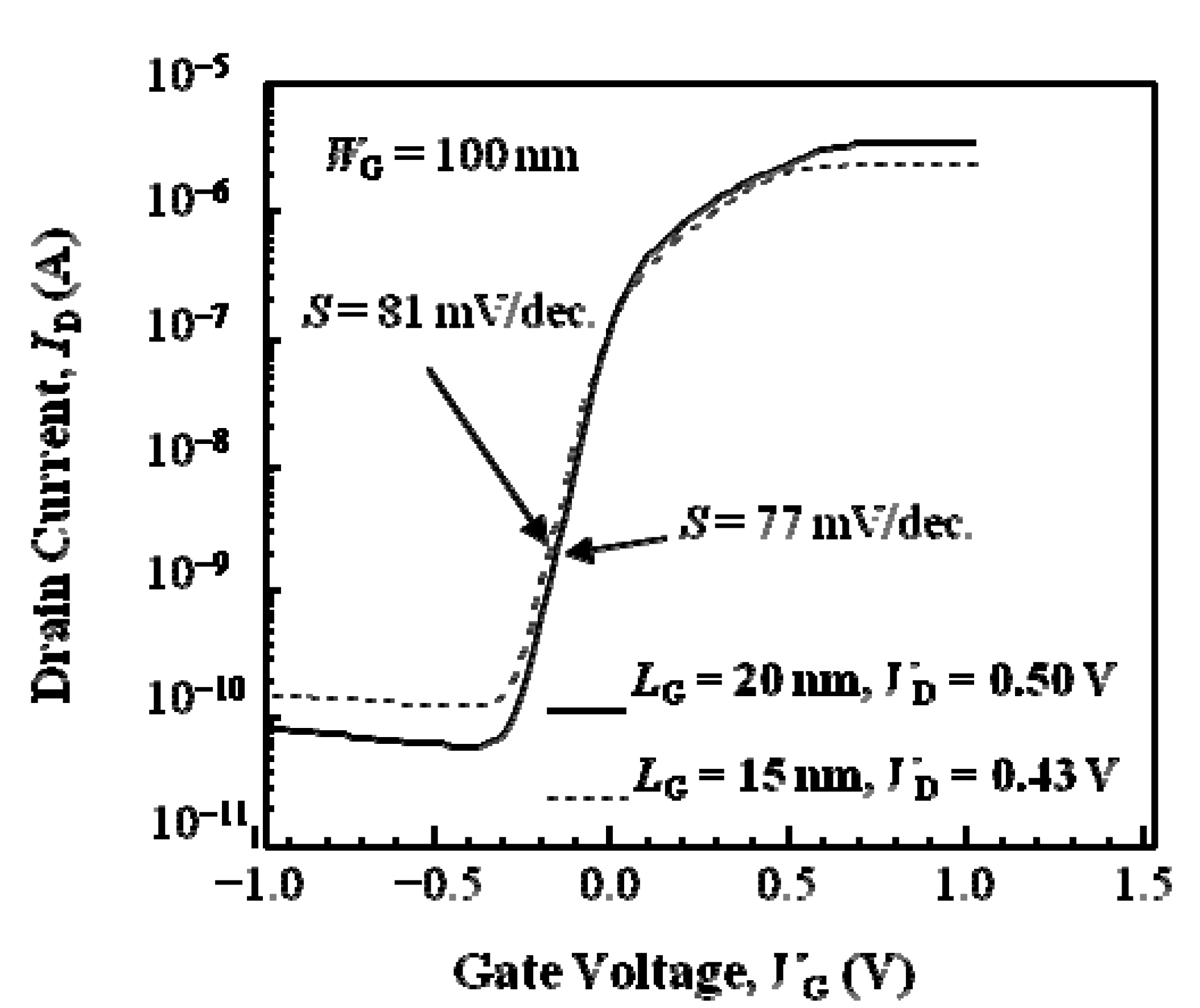
Simulated subthreshold characteristics of the 15-nm-long gate XCT-SOI MOSFET and the 20-nm-long gate XCT-SOIMOSFET are compared in
Figure 7; both devices have the abrupt junctions. It is seen in
Figure 7 that the subthreshold swing (
S) is 77 mV/dec, for the 20-nm-long gate device, and 81 mV/dec, for the 15-nm-long gate device. Short-channel effects are well suppressed. However, the gate-induced drain-leakage (GIDL) current level of the 15-nm-long gate XCT-SOI device is somewhat high (~10
−9 A/μm) as the device simulation assumes the abrupt junction for simplicity.
Figure 6.
Simulation results of ID-VD characteristics of 15-nm-long gate XCT-SOI MOSFET. L denotes the effective channel length.
Figure 6.
Simulation results of ID-VD characteristics of 15-nm-long gate XCT-SOI MOSFET. L denotes the effective channel length.
Figure 7.
Simulation results of ID-VG characteristics of 20-nm-long and 15-nm-long gate XCT-SOI MOSFET. It is assumed that the devices have abrupt source and drain junctions.
Figure 7.
Simulation results of ID-VG characteristics of 20-nm-long and 15-nm-long gate XCT-SOI MOSFET. It is assumed that the devices have abrupt source and drain junctions.
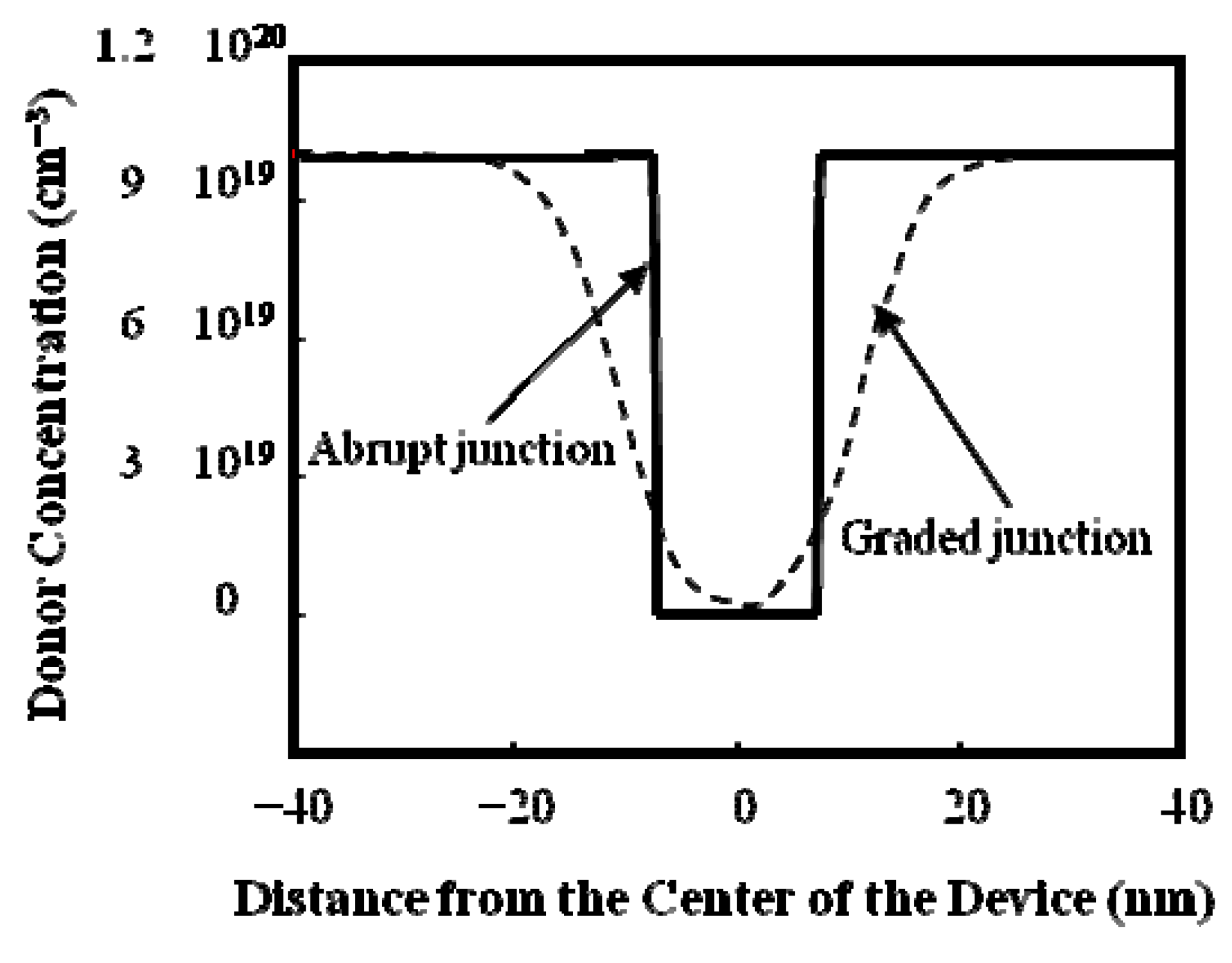
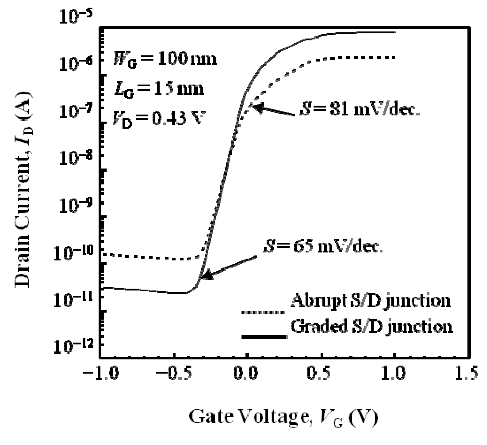
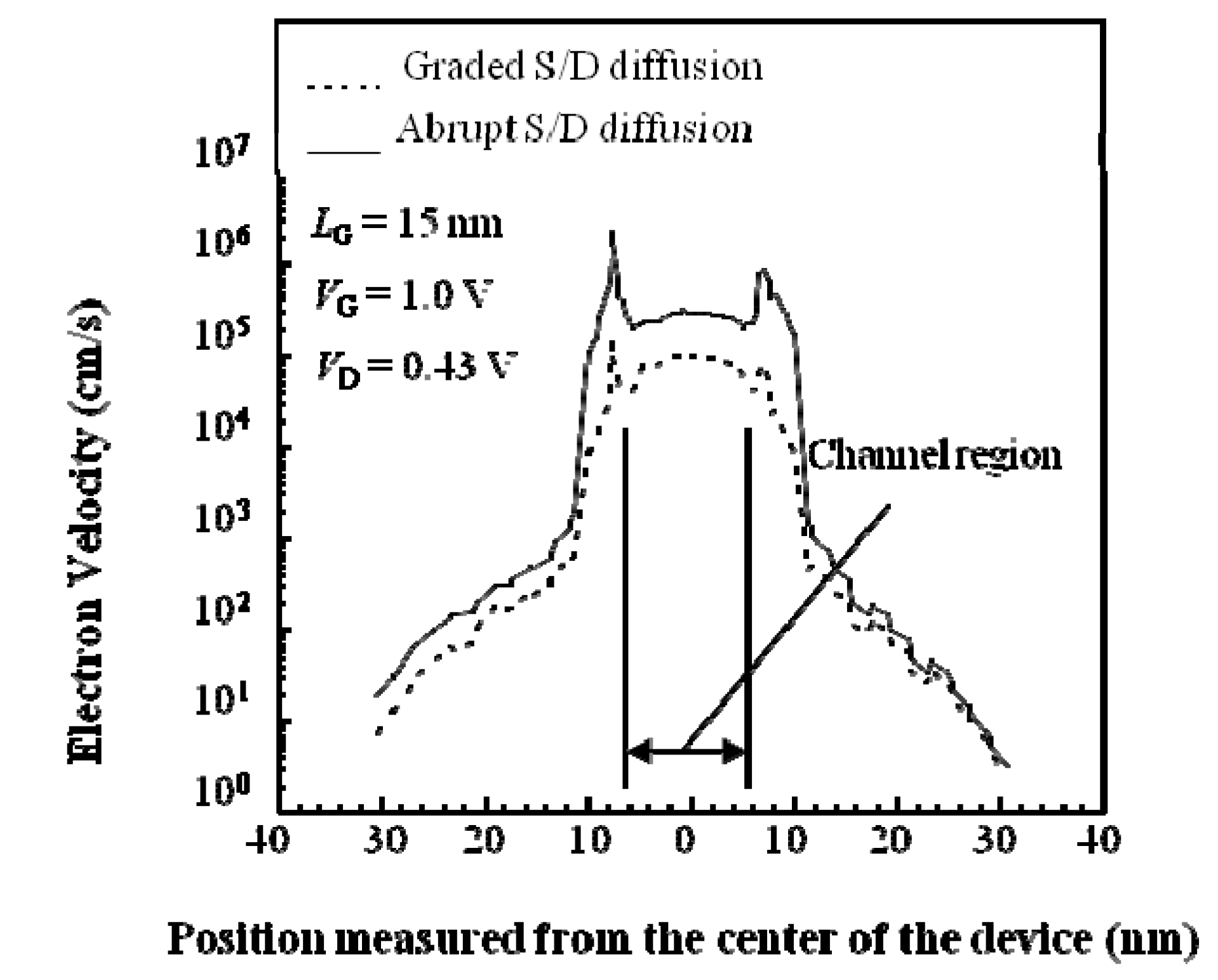
In response, we introduced a 10-nm-long graded doping region for source and drain junctions as a “new” scaling scheme, as shown in
Figure 8. Simulated
ID-VG characteristics of the 15-nm-long gate XCT-SOI MOSFET are shown in
Figure 9. Drain current characteristics of 15-nm-long gate XCT-SOI devices with the abrupt and the graded junctions are compared. It should be noted that the subthreshold swing is 65 mV/dec for the 15-nm-long gate device with the graded junction. Short-channel effects are well suppressed in the 15-nm-long gate XCT-SOI MOSFET. The GIDL current level is lowered to 200 pA/μm. The most noticeable result is the improved drivability of the device with the graded junction; this is due to the remarkable improvement in carrier velocity over the whole device region, as shown in
Figure 10 [
13], and the reduction of the channel resistance of the parasitic pJFET [
12].
Figure 8.
Doping profiles from the source to drain. The doping profile with a graded junction is compared to that with an abrupt junction.
Figure 8.
Doping profiles from the source to drain. The doping profile with a graded junction is compared to that with an abrupt junction.
Figure 9.
Simulation results of ID-VG characteristics of 15-nm-long gate XCT-SOI MOSFET. Impact of doping profile on ID-VG characteristics is compared.
Figure 9.
Simulation results of ID-VG characteristics of 15-nm-long gate XCT-SOI MOSFET. Impact of doping profile on ID-VG characteristics is compared.
Figure 10.
Simulation results of carrier velocity along the channel for the 15-nm-long gate XCT-SOI MOSFET. Impact of doping profile on velocity profile is compared.
Figure 10.
Simulation results of carrier velocity along the channel for the 15-nm-long gate XCT-SOI MOSFET. Impact of doping profile on velocity profile is compared.
6. Conclusions
We demonstrated the low-energy operation of XCT-SOI CMOS devices scaled down to 15 nm and analyzed the key underlying mechanism. It was shown that the source-follower like operation of the XCT-SOI MOSFET dynamically reduces the effective input capacitance, and, thus, the energy dissipated by XCT-SOI devices. This operation should be called the “source potential floating effect (SPFE)”. It is predicted, based on a physics-based model, that realizing SPFE in XCT-CMOS circuits will significantly suppress standby power dissipation.
It was also suggested that such aspects are still available in the sub-30-nm-long gate regime. Therefore, we can state that XCT-SOI CMOS devices are very promising for future extremely-low-energy circuits that suit medical implant applications.


