1. Introduction
Many physical conditions and diseases of the heart can be non-invasively detected through feature extraction from ECG. Significant features of the ECG signal include the P-wave, Q, R, and S waves (QRS) complex and T-wave. The P-wave represents atrial depolarization, the QRS complex left ventricular depolarization and the T-wave left ventricular repolarization. Thus, analysis of the T-wave in the ECG is an essential clinical tool for diagnosis, monitoring and follow-up of patients with heart dysfunction [
1,
2].
In order to sense the T-wave, a low pass filter with a cutoff frequency of 2.4 Hz should be realized. According to [
3], a suitable choice is a sixth-order Bessel filter, and this originates from the fact that this type of filter offers an equal delay of all of the pass band frequencies without affecting the shape of the filtered signal. The topology in [
3] operates under a ±1.5-V supply voltage and has been implemented using operational transconductance amplifiers (OTAs) as active elements, where the small signal transconductance parameter (g
m) has been employed for realizing the required time constants. The scheme in [
4] has been realized using the concept of sinh-domain filtering, and therefore, the large signal characteristic of transistors has been used for the realization of time constants without the requirement of extra linearization stages. The employed supply voltage for this topology was ±1 V.
A sixth-order low pass filter topology is presented in this paper, realized using the concept of sinh-domain filtering. The reason is that sinh-domain filters have inherent class-AB operation, which allows biasing at current levels significantly lower than that of the maximum signal that can be handled by the system. In addition, the employment of MOS transistors in the subthreshold region offers the advantage of reduced power consumption [
5,
6,
7]. The topology operates in a 0.5-V supply voltage environment. A value of dynamic range (DR) equal to 51.1 dB has been achieved under this ultra-low voltage environment, and according to the provided comparison results, the proposed topology offers the most power-efficient realization among the filters under consideration. The paper is organized as follows: the basic building blocks are presented in
Section 2, while the performance of the filter topology is evaluated in
Section 3 through a comparison with the corresponding already published counterparts. Simulations have been performed using the Cadence Virtuoso Analog Design Environment and MOS transistor models provided by the AMS C35 0.35-µm CMOS process.
2. Building Blocks for Sinh-Domain Filtering
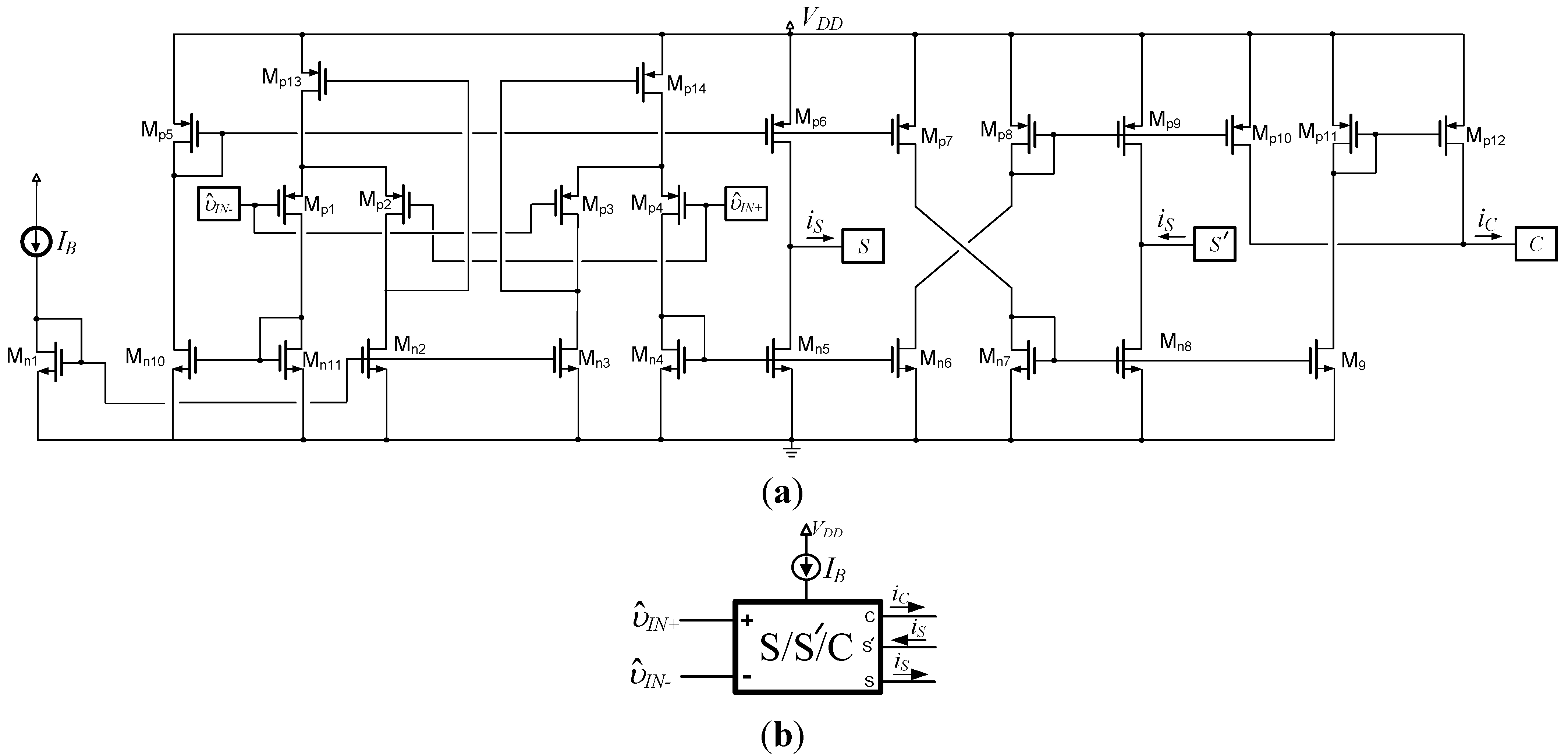
Non-linear transconductors are the basic building block for realizing sinh-domain circuits. A typical multiple-output non-linear transconductor cell is depicted in
Figure 1a, while the corresponding symbol is given in
Figure 1b. Assuming that the MOS transistors operate in the subthreshold region, the expressions of output currents of the transconductor are given by Equations (1) and (2)
where
IB is the bias current of the transconductor,
n is the subthreshold slope factor (1 <
n < 2) of the MOS transistor,
VT is the thermal voltage (≈26 mV at 27 °C) and
,
are the voltages at the non-inverting and inverting inputs, respectively [
5,
6,
7].
Figure 1.
Multiple-output non-linear transconductor (S/S’/C cell) (a) circuitry; and (b) symbols.
Figure 1.
Multiple-output non-linear transconductor (S/S’/C cell) (a) circuitry; and (b) symbols.
Due to the employment of the current-mirror constructed from transistors, Mn7–Mn8 and Mp8–Mp9, the current at the S' terminal is an inverted replica of that at the S terminal. Consequently, the expression in Equation (1) is still valid for this current.
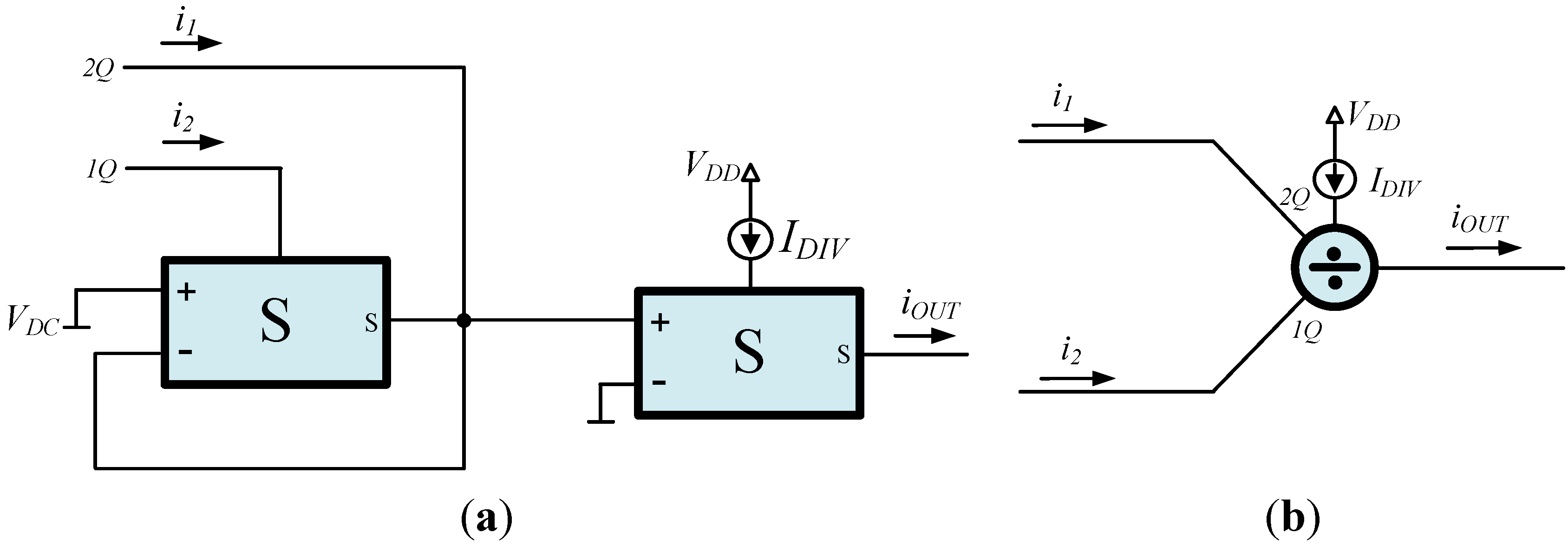
The realization of a two-quadrant divider, using single output non-linear transconductor cells, derived from the general topology in
Figure 1a by omitting the S' and C outputs, is depicted in
Figure 2. The expression for the output current is given by the formula
iOUT =
IDIV (
i1/
i2), where
IDIV is the bias current of the divider and
i1 and
i2 are two and one-quadrant input currents, respectively [
5,
6,
7].
Figure 2.
Two-quadrant divider (a) realization using S cells; and (b) symbols.
Figure 2.
Two-quadrant divider (a) realization using S cells; and (b) symbols.
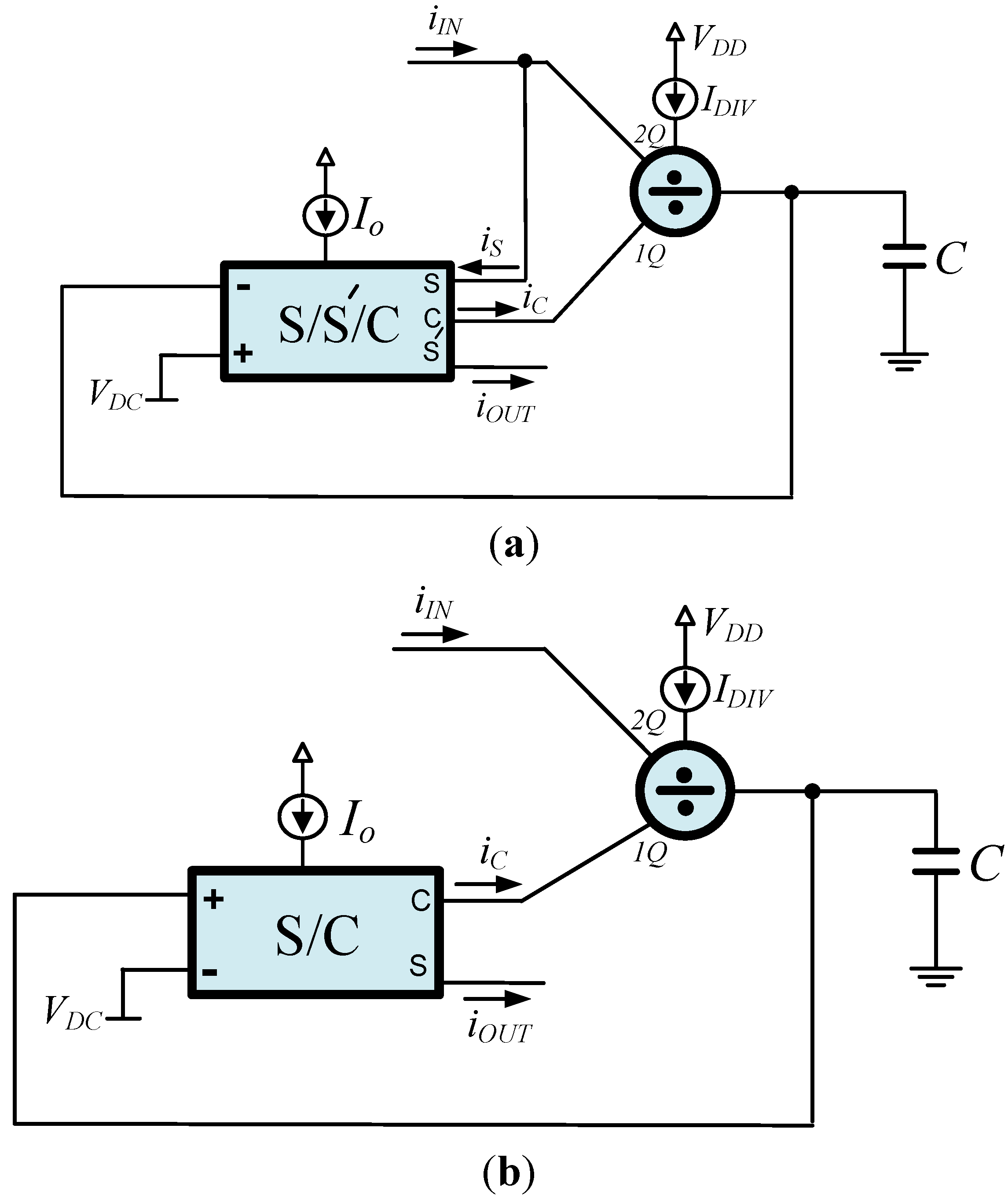
Using the building block in
Figure 1, the topology of a lossy (
i.e., first-order filter) sinh-domain integrator is demonstrated in
Figure 3a, while in
Figure 3b, the topology of a lossless integrator is given. The realized transfer functions are given by (3) and (4), respectively, as:
where the time-constant in both of them is:
An important benefit offered by the topologies in
Figure 3 is that the time constant can be electronically adjusted through the DC bias current
IDIV without disturbing the DC current
Io used for biasing the multiple-output transconductors. In other words, an orthogonal adjustment between
IDIV and
Io is possible, and as a result, relatively large time constants can be realized without affecting the level of currents that can be successfully handled by the system [
8,
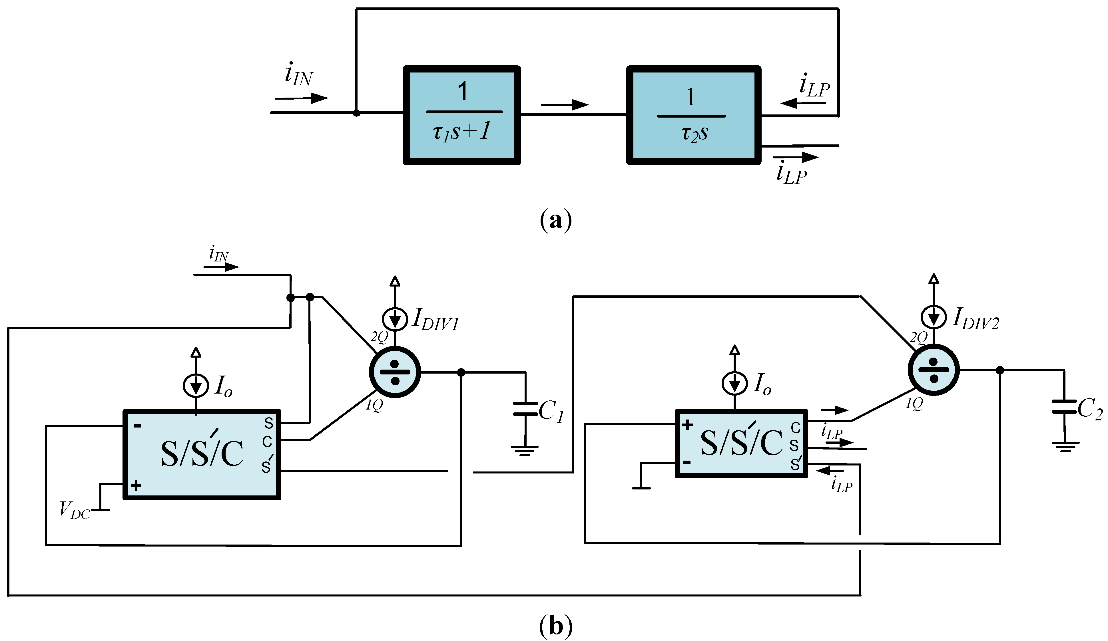
9].The functional block diagram (FBD) of a second-order low pass filter implemented through the utilization of a two-integrator loop is given in
Figure 4a, while the corresponding sinh-domain realization derived using the integrators in
Figure 3 is demonstrated in
Figure 4b.
Figure 3.
Sinh-domain integrators (a) lossy; and (b) lossless.
Figure 3.
Sinh-domain integrators (a) lossy; and (b) lossless.
Figure 4.
Second-order low pass filter (a) functional block diagram; and (b) realization using the concept of sinh-domain filtering.
Figure 4.
Second-order low pass filter (a) functional block diagram; and (b) realization using the concept of sinh-domain filtering.
The realized transfer function is:
According to Equation (6), the resonant frequency and the
Q factor of the filter are given by Equations (7) and (8), respectively, as:
Using Equation (5), the expressions in Equations (7) and (8) could be written as:
3. Comparison Results and Biomedical Application Example
The sixth-order low pass filter will be realized through a cascade connection of second-order blocks given in
Figure 4b. MOS transistor models provided by the AMS 0.35-μm C35 CMOS process, as well as the Cadence Virtuoso Analog Design Environment will be employed. The bias scheme was
VDD = 0.5 V,
VDC = 100 mV and
Io = 100 pA. Considering that the MOS transistors operate in the subthreshold region, the corresponding aspect ratios for the non-linear transconductor in
Figure 1a are summarized in
Table 1. The capacitor values, as well as the bias currents of dividers for all stages of the system are given in
Table 2.
Table 1.
MOS transistor aspect ratios for the non-linear transconductor in
Figure 1.
Table 1.
MOS transistor aspect ratios for the non-linear transconductor in Figure 1.
| Transistor | W/L (μm/μm) |
|---|
| MP1–ΜP12 | 60/1 |
| Mp13–Μp14 | 20/0.4 |
| Mn1–Μn11 | 8/1 |
Table 2.
Bias scheme and capacitor values for the stages of the sixth-order low pass filter.
Table 2.
Bias scheme and capacitor values for the stages of the sixth-order low pass filter.
| Stage | Values |
|---|
| Low Pass filter #1 | VDD = 0.5 V, VDC = 0.1 V, Io = 100 pA |
| IDIV1 = 15.9 pA, IDIV2 = 8.24 pA |
| C1 = 10 pF, C2 = 20 pF |
| Low Pass filter #2 | VDD = 0.5 V, VDC = 0.1 V, Io = 100 pA |
| IDIV1 = 13.9 pA, IDIV2 = 10.4 pA |
| C1 = 10 pF, C2 = 20 pF |
| Low Pass filter #3 | VDD = 0.5 V, VDC = 0.1 V, Io = 100 pA |
| IDIV1 = 9.3 pA, IDIV2 = 9.8 pA |
| C1 = 10 pF, C2 = 10 pF |
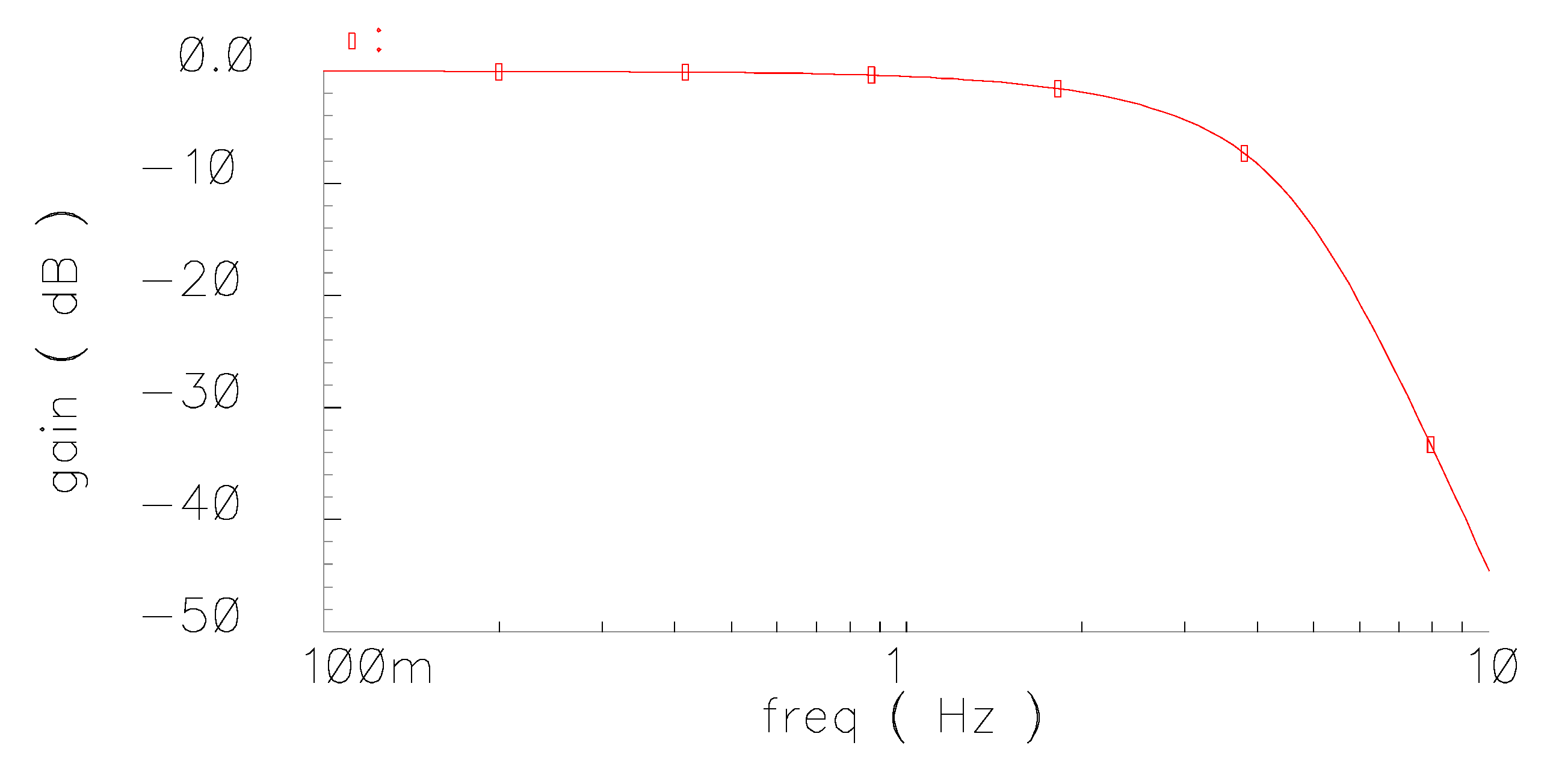
The DC power dissipation of the filter was 7.21 nW. The obtained frequency response is demonstrated in
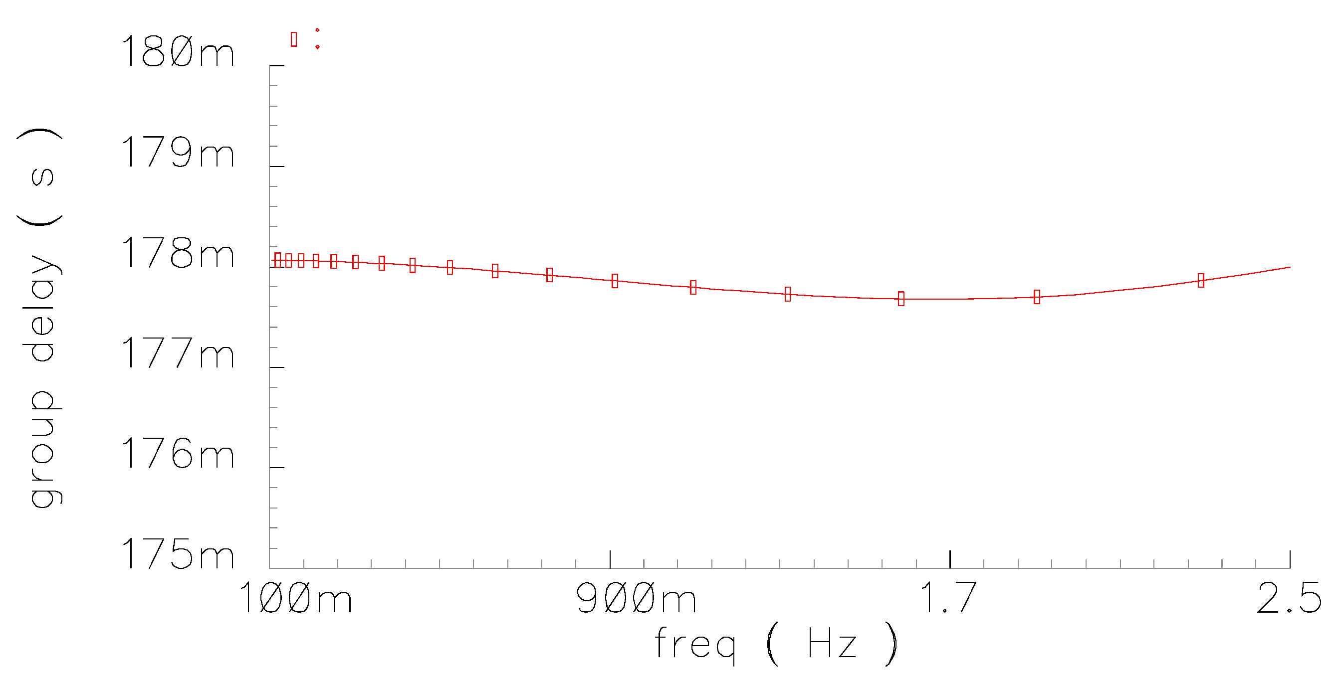
Figure 5, where the achieved cutoff frequency was 2.4 Hz. The group delay as a function of frequency is plotted in
Figure 6. The group delay error within the pass band was 0.2%.
Figure 5.
Gain vs. frequency (freq) of the sixth-order Bessel low pass filter.
Figure 5.
Gain vs. frequency (freq) of the sixth-order Bessel low pass filter.
Figure 6.
Group delay variation of the sixth-order Bessel low pass filter within the pass band.
Figure 6.
Group delay variation of the sixth-order Bessel low pass filter within the pass band.
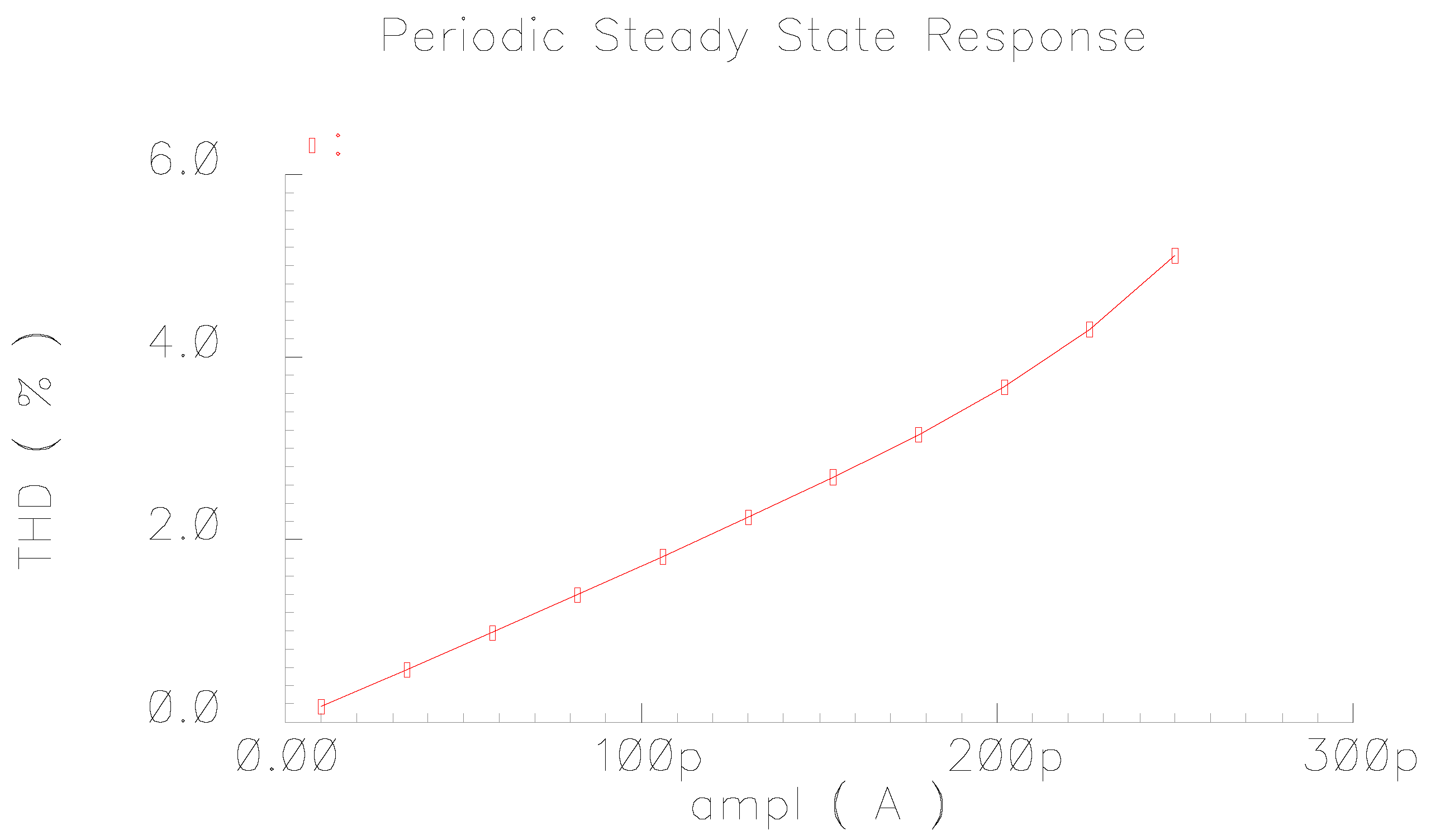
Figure 7.
Total harmonic distortion (THD) vs. amplitude (ampl) of the input signal.
Figure 7.
Total harmonic distortion (THD) vs. amplitude (ampl) of the input signal.
The linear performance of the filter has been evaluated by stimulating its input with a sinusoidal signal with frequency of 0.5 Hz and variable amplitude. The obtained total harmonic distortion (THD) plot is depicted in
Figure 7, where THD levels equal to 2% and 4% are achieved for amplitudes of 120 and 220 pA, respectively. The noise has been integrated within the pass band of the filter and the input referenced RMS value of noise was 0.43 pA. For comparison purposes, the input signal that corresponds to a THD level of 4% has been considered, and the predicted value of the DR of the filter is 51.1 dB.
The sensitivity of the filter with regards to the effect of MOS transistors mismatch, as well as process parameter variations has been evaluated using Monte-Carlo analysis offered by the Cadence Analog Design Environment. The derived statistical plots for 100 runs are given in
Figure 8. The standard deviation of the low frequency gain was 0.13, whereas that of the bandwidth was 0.4 Hz. Therefore, the proposed filter topology offers reasonable sensitivity characteristics.
Figure 8.
Monte-Carlo analysis results for (a) low-frequency gain; and (b) the bandwidth (bw) of the low pass filter.
Figure 8.
Monte-Carlo analysis results for (a) low-frequency gain; and (b) the bandwidth (bw) of the low pass filter.
A performance comparison has been done between the proposed filter and those already introduced in [
3,
4]. The obtained results are summarized in
Table 3, where the power efficiency of the topologies under consideration has been evaluated through the employment of the figure of merit (
FoM) defined by Equation (11) as:
where
P is the power dissipation of the filter,
n the number of poles,
fo the cutoff frequency and
DR the dynamic range. According to the results in
Table 3, the proposed filter simultaneously offers the benefits of ultra-low voltage operation and power efficiency.
The behavior of the system has been evaluated using the artificial ECG signal depicted in
Figure 9a, obtained from the Massachusetts Institute of Technology/Beth Israel Hospital (MIT/BIH) database [
10]. The resulting waveform of the filtered signal is demonstrated in
Figure 9b, where it is easily observed that it is very close to that theoretically predicted. In order to facilitate the comparison, both input and output waveforms are simultaneously given in the plot of
Figure 9c, where the effectiveness of the proposed system for sensing the T-wave of an ECG is readily verified.
Figure 9.
Waveforms of: (a) input ECG signal; (b) filtered output (red: ideal, blue: real); and (c) input-output.
Figure 9.
Waveforms of: (a) input ECG signal; (b) filtered output (red: ideal, blue: real); and (c) input-output.
Table 3.
MOS transistor aspect ratios for the non-linear transconductor in
Figure 1.
Table 3.
MOS transistor aspect ratios for the non-linear transconductor in Figure 1.
| Performance characteristics | LP filter in [3] | LP filter in [4] | LP filter in this work |
|---|
| Technology | 0.8 µm CMOS | 0.35 µm CMOS | 0.35 µm CMOS |
| Power supply voltage | ±1.5 V | ±1 V | 0.5 V |
| Order of filter | 6 | 6 | 6 |
| Power dissipation | 10 µW | 1.5 µW | 7.21 nW |
| Cutoff frequency | 2.4 Hz | 2.4 Hz | 2.4 Hz |
| Total capacitance | - | 120-300 pF | 80 pF |
| Dynamic range | 60 dB (0.5% THD) | 66 dB (4% THD) | 51.1 dB (4% THD) |
| Group delay error within pass band | - | 0.2% | 0.2% |
| Figure of merit | 694 pJ | 52.2 pJ | 1.4 pJ |
| Standard deviation of gain | - | - | 0.13 |
| Standard deviation of bandwidth | - | - | 0.4 Hz |
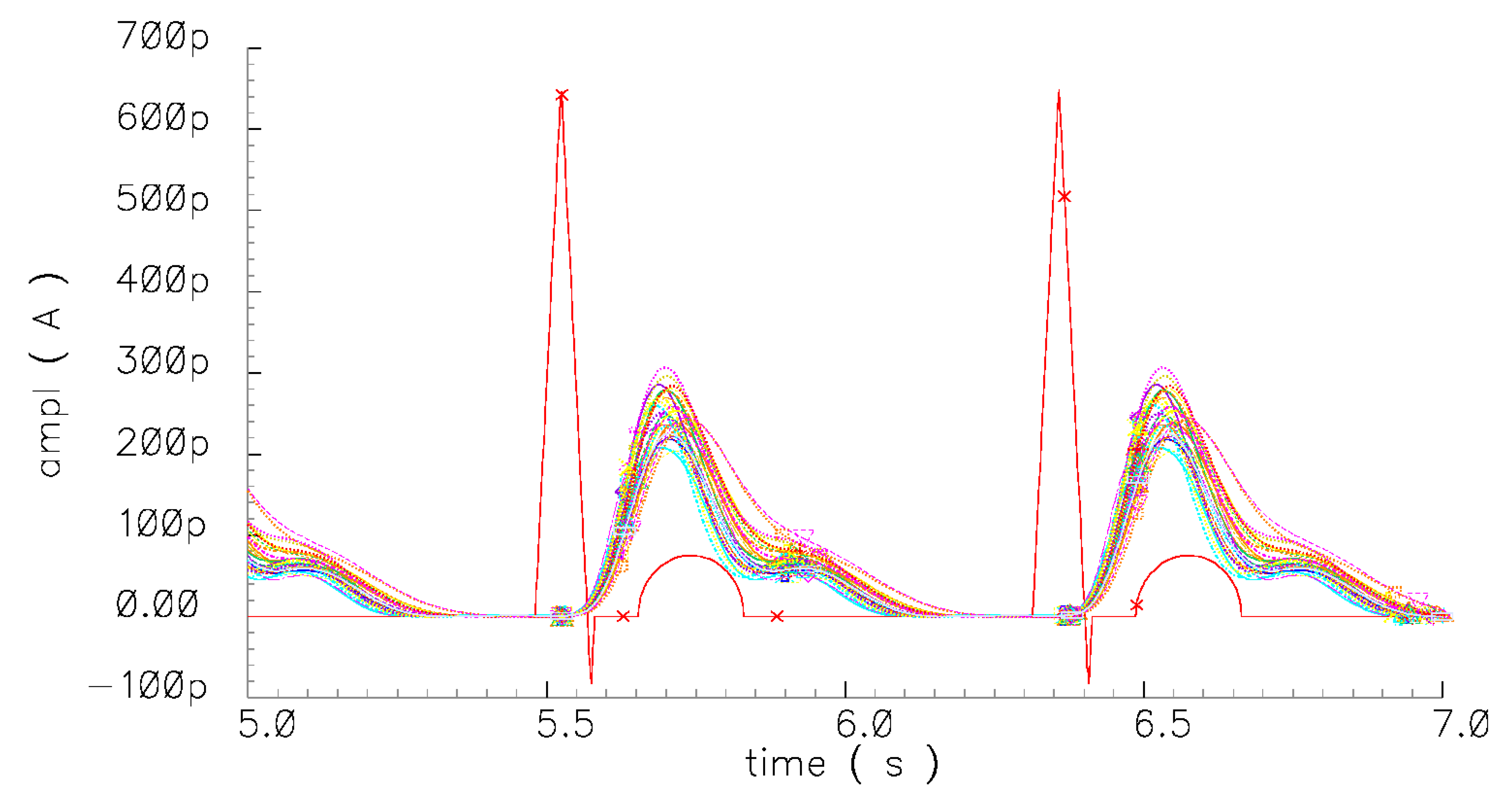
In order to verify the robustness of the design, the effect of process variations has been considered through the utilization of Monte-Carlo analysis. The derived output waveforms are demonstrated in
Figure 10, where it is evident that the proposed filter preserves its effectiveness for sensing the T-wave of an ECG.
Figure 10.
Output waveforms obtained through Monte-Carlo analysis.
Figure 10.
Output waveforms obtained through Monte-Carlo analysis.
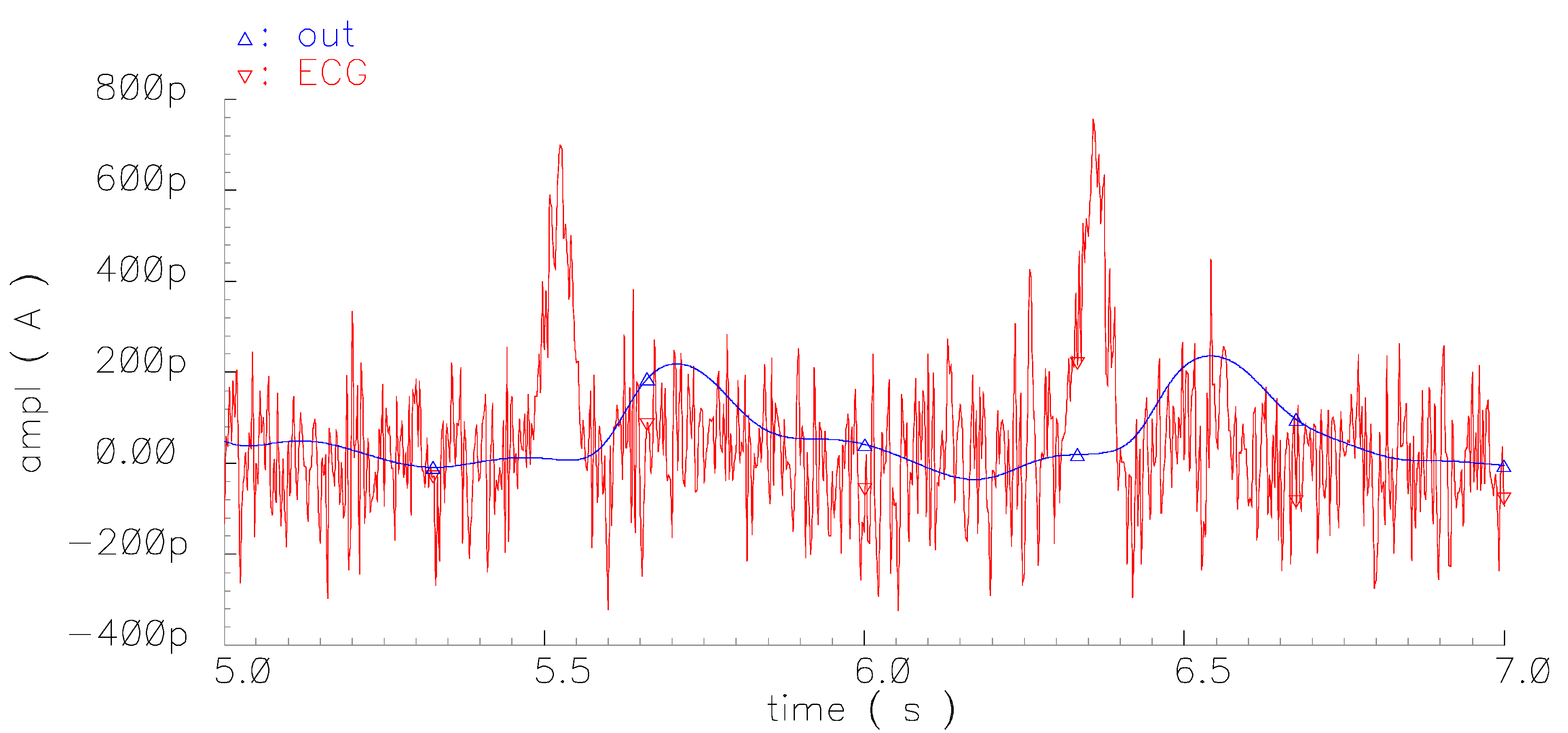
The performance of the proposed filter topology has been also evaluated with regards to the effect of noise. For this purpose, a noisy ECG has been obtained from that in
Figure 9a through the addition of Gaussian noise (bandwidth 180 Hz), with a signal-to-noise ratio (SNR) equal to 0 dB, and has been employed as a stimulus for the filter. The derived output waveform is depicted, simultaneously with the input noisy ECG signal, in
Figure 11, where it is evident that the filter is capable of detecting the T-wave of a noisy ECG.
Figure 11.
Output waveform of the filter stimulated by a noisy ECG.
Figure 11.
Output waveform of the filter stimulated by a noisy ECG.


