1. Introduction
The Internet-of-Things (IoT) demands ubiquitous devices that collect and process sensed data and transmit back to the central node through various network interfaces [
1]. Since radio devices usually dominate the power consumption of the system [
2], in biomedical or physiological monitoring, the sensor data at each node should be preprocessed before transmission [
3]. In particular, biomedical sensors in the IoT targets an important application of the “unmanned medical nursing system” [
1], which could alleviate increasing medical costs as the baby boomers enter retirement [
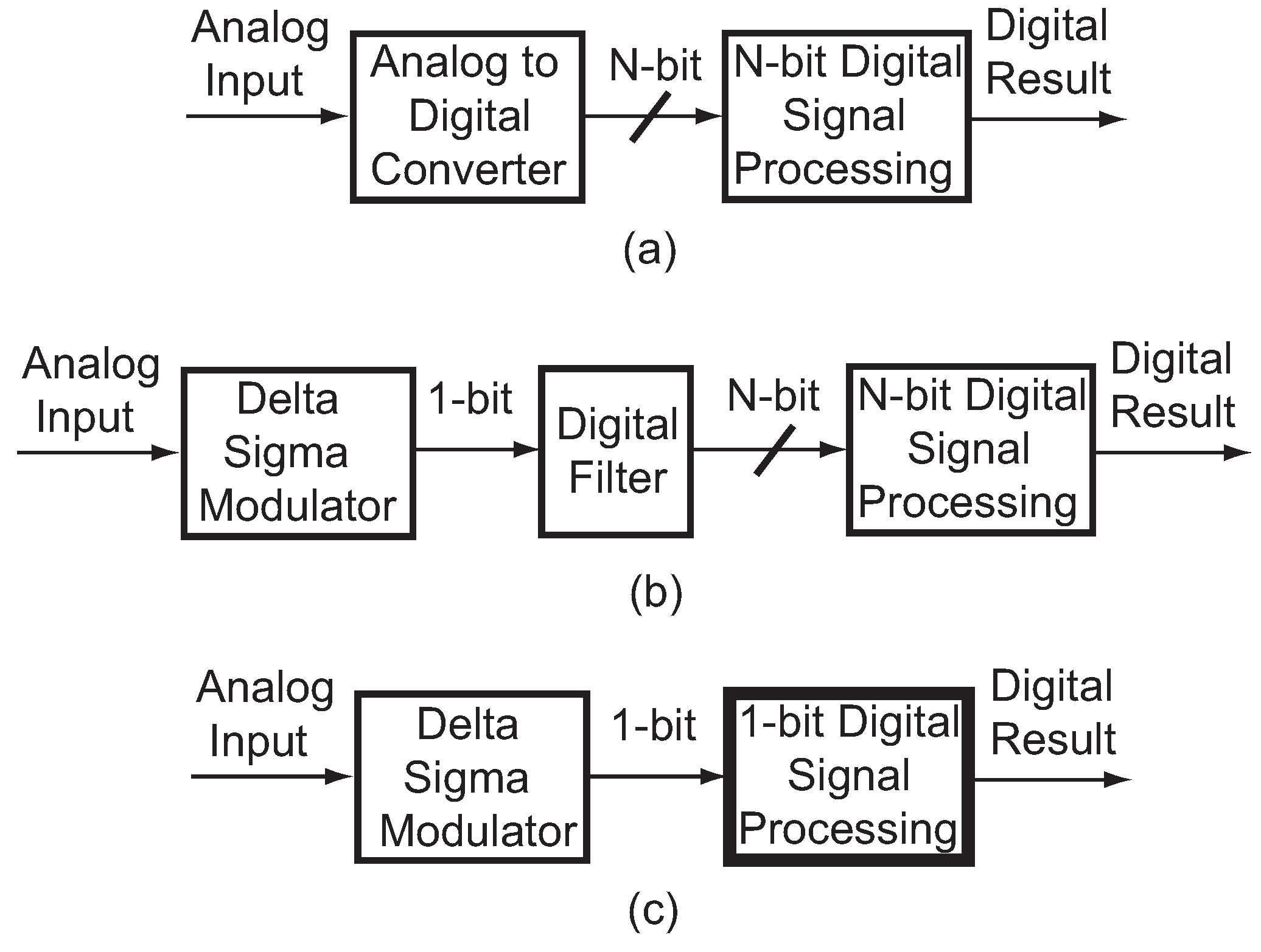
4]. Such wearable and implantable biomedical sensors demand low-complexity, low-power, high-resolution and high-reliability digital signal processing (DSP) circuits, which present the need to enhance the currently-applied solution. In a typical biomedical sensor, the recorded analog signal is first converted into digital format and then processed by an application-specific integrated circuit (ASIC) processor running a pre-implemented DSP algorithm, as shown in
Figure 1a. If the algorithm determines that the incoming signal is abnormal, then the ASIC sends an alert signal and calls for help through wireless portable devices via the IoT. In such a system, the major challenges are the relatively large circuit area and high power of the DSP circuits performing multiply-and-accumulate (MAC) operations [
5], which are adders and coefficient multipliers in digital filters. In order to miniaturize the physical size and extend the battery life of the circuits, low-complexity low-power designs are very important. As an example, in [
5], an eight-channel 10-bit resolution DSP seizure detector processor consumes more than 50% of the chip area and power in a 5 mm × 5 mm system-on-a-chip (SOC) implemented in a 65-nm process, even though a look-up table (LUT) method is applied, which saved more than 50% of the total gate count in the digital filters [
6]. Besides circuit complexity and power consumption, such circuits demand higher resolution and reliability, since higher resolution improves accuracy, and reliability is the key issue in biomedical applications. However, if a higher resolution circuit is implemented, then the power, chip area and cost of the DSP circuits also increase.
Figure 1.
(a) Traditional signal processing architecture; (b) traditional signal processing after a Delta Sigma ADC; (c) the proposed signal processing using a Delta Sigma digital signal processing (DSP).
Figure 1.
(a) Traditional signal processing architecture; (b) traditional signal processing after a Delta Sigma ADC; (c) the proposed signal processing using a Delta Sigma digital signal processing (DSP).
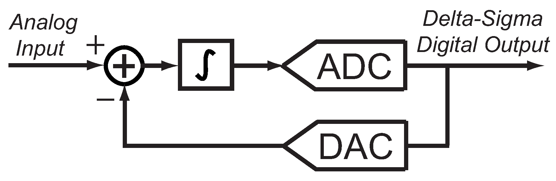
Delta Sigma technology can be an attractive solution for the aforementioned challenges and has been widely applied in biomedical circuits and systems [
7,
8,
9,
10,
11,
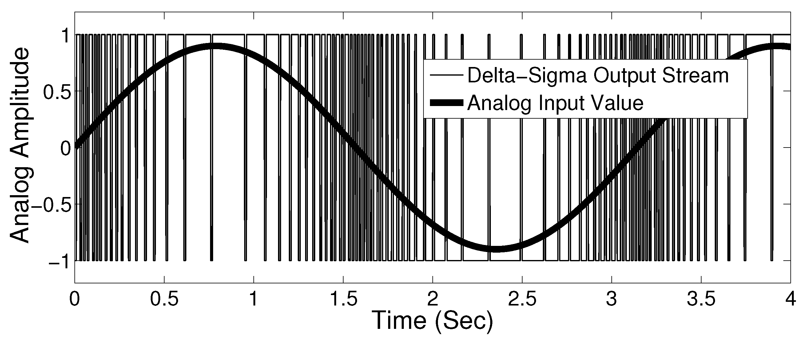
12] because of its unique properties. First, it is well known that a Delta Sigma analog-to-digital converter (ADC) has much less circuit complexity and lower power consumption than multi-bit ADCs. Second, in the Delta Sigma domain, the instantaneous analog value is represented by the moving average of the Delta Sigma bit-stream. Therefore, a few bit errors in the bit-stream do not disturb the signal level greatly [
13]. Therefore, Delta Sigma systems have a higher tolerance to bit errors than multi-bit binary systems, which means Delta Sigma systems have higher reliability. Third, an oversampling Delta Sigma ADC can achieve a higher resolution (up to 24 bits) compared to a Nyquist rate multi-bit ADC (usually less than 18-bits). The Delta Sigma ADCs also relax the requirements on the analog anti-aliasing filter. Moreover, the resolution of a Delta Sigma system can be flexibly changed by adjusting its clock rate, without modifying the hardware. On the other hand, concerns for using a Delta Sigma system usually arise from its higher sampling rate and larger data size. However, in biomedical applications, the input signal usually has a bandwidth less than 2 kHz. Furthermore, the storage of raw data is usually neither necessary nor easily implementable. Thus, in such applications, using Delta Sigma bit-streams to represent and process information is both applicable and desirable.
Although Delta Sigma technology has been widely used in converting analog signals to digital signals [
7,
9,
11], it has not been commonly applied in DSP, because of the lack of Delta Sigma-based DSP circuits. Currently, the modulated Delta Sigma bit-stream is demodulated into a multi-bit stream and then processed by conventional multi-bit DSP circuits, as shown in
Figure 1b [
14]. However, hardware complexity, power and reliability issues limit the performance of the multi-bit DSP system. Here, we study the alternative method using a one-bit DSP system to process Delta Sigma bit-streams directly, as shown in
Figure 1c.
Currently, Delta Sigma-based DSP circuits are not sufficiently studied. In DSP systems, the most important linear circuits are sum adders, average adders and coefficient multipliers. To build those circuits with low noise and complexity, pure digital implementations are preferable. However, some previous Delta Sigma processing methods focused on modifying the Delta Sigma modulators [
15,
16,
17] instead of processing the modulated bit-stream. Moreover, some solutions are hindered by involving analog operations [
18,
19,
20] or tri-state digital circuits [
21], which increase the complexity of the circuits. Other designs are impeded by their ability to process only first-order Delta Sigma bit-streams [
22,
23,
24,
25,
26,
27,
28,
29,
30,
31,
32,
33], which do not fit the widely-used higher-order Delta Sigma modulators. Furthermore, the adders in [
22] can only take two inputs. One method of processing higher order Delta Sigma bit-streams is the digital Delta Sigma modulator proposed. However, a digital Delta Sigma modulator designed with a complicated sorting network [
13] requires enormous circuit resources, which is not applicable for low-power devices.
In this paper, we propose novel methods and circuits for Delta Sigma-based DSP systems. Based on the digital Delta Sigma modulator method and the proposed
P-N (positive-negative) pair method with a signed binary counter, we design the Delta Sigma sum adder, average adder and coefficient multiplier. We also present simulation and measurement results of the proposed circuits and provide a comparison of the synthesis results between Delta Sigma adders and multi-bit binary adders. This paper is organized as follows:
Section 2 presents the properties of a first-order Delta Sigma modulated bit-stream and the basic processing techniques using the proposed
P-N pair method. In
Section 3, we describe the design of the Delta Sigma sum adder and the average adder.
Section 4 provides simulation and analysis of the Delta Sigma adders.
Section 5 describes a Delta Sigma compressor design.
Section 6 presents the implementation and measurement results of the Delta Sigma average adder.
Section 7 compares the proposed Delta Sigma adders to conventional multi-bit adders.
Section 8 concludes the paper.
3. Delta Sigma Adders
In this section, we introduce Delta Sigma adders using the proposed P-N pair method. Adding is a basic linear operation, which is indispensable in DSP. There are two types of adders in DSP: sum adders and average adders. In Delta Sigma processing, a sum adder generates a new Delta Sigma bit-stream based on the input bit-streams. The analog value of the output bit-stream is equal to the sum of the analog values of the addend bit-streams. On the other hand, an average adder generates a bit-stream whose analog value is equal to the average of all of the analog values of the addend bit-streams.
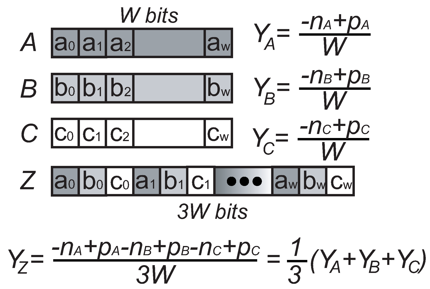
Here, we show a basic example of adding Delta Sigma bit-streams. An average bit-stream can be simply created by mixing all of the addend bit-streams bit by bit. As shown in
Figure 5, the output bit sequence
Z is generated by mixing input bit sequences
A,
B and
C. Here, the analog value of
Z is 1/3 of the sum (
y +
y +
y). However, its length is three-times that of one addend. Therefore,
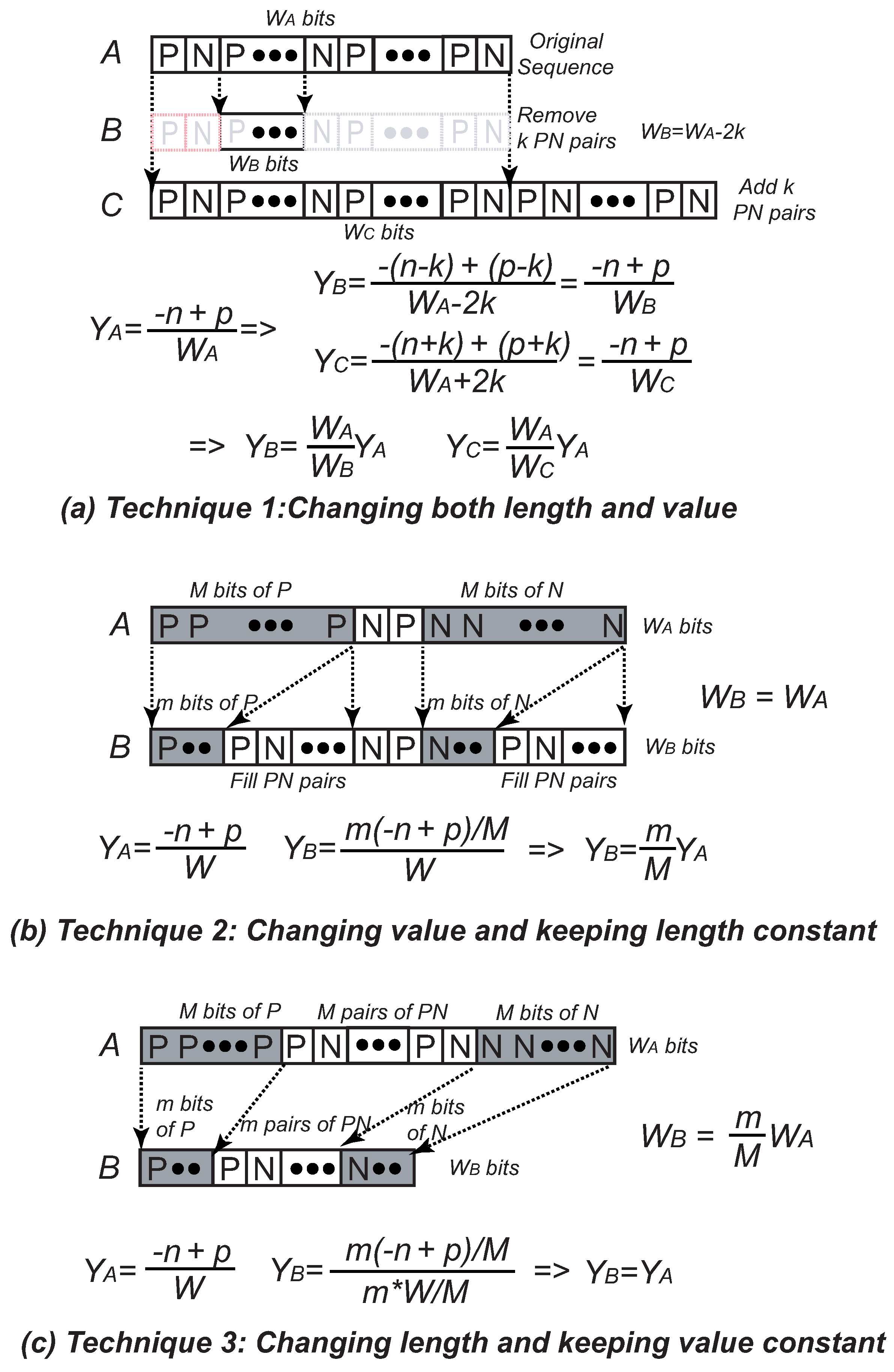
Z requires a three-times faster clock than the addend bit-streams. In order to obtain the output bit-stream with the same data rate of the input bit-streams, the length of the mixed bit-stream must be reduced. This can be done using Technique 3 in
Section 2 by deleting
P-N pairs and homogeneous bits from the mixed bit sequence until the output bit sequence has the same length of the addends. This keeps the analog value while reducing the length of the bit sequence. On the other hand, by applying Technique 1 in
Section 2, we can reduce the length of the bit sequence by three while increasing its analog value by three, thus removing the coefficient 1/3 and obtaining the sum bit sequence.
An on-the-fly processing circuit can be designed to perform the aforementioned processing of long combined bit-streams. The basic idea of an on-the-fly Delta Sigma adder is to remove
P-N pairs simultaneously from the addend Delta Sigma bit-streams in order to keep the data rate of the sum bit-stream the same as that of the addends. This requires counting the number of
P and
N bits from all addends in each clock cycle. A counter performs the on-the-fly operation based on:
In Equation (
2),
Y is the counting result.
X is the instantaneous bit of the
i-th input bit-stream, and
M is the number of addends. To make a
P bit cancel an
N bit,
X equals +1 if the input bit is
P, while
X equals −1 if the input bit is
N. This guarantees that
P-N pairs can be removed from the result.
Y represents the number of the surplus of either
P bits or
N bits. Thus, the result
Y is either a zero, a positive number or a negative number. We use a signed binary number, for example the two’s complement format, to represent the result
Y.
Nevertheless, since +1 and −1 are applied in Equation (
2), the system requires dual power supplies or a tri-state digital system similar to [
21], which is not compatible with current two-state digital systems. We need a counter that can work in a two-state digital system. To make
X compatible with the commonly-used binary system, we modify Equation (
2) to get:
In Equation (
3)
X equals one if the input bit is
P or equals zero if the input bit is
N. A binary counter for calculating Equation (
3) can be realized using an
M-input one-bit binary adder in a two-state digital system. Here, a positive value of the
Y’ means
Y’ P bits remain after removing
P-N pairs from all of the input bits, while a negative value of the
Y’ means −
Y’ N bits remain.
Figure 5.
Averaging of the Delta Sigma bit-streams by mixing bits.
Figure 5.
Averaging of the Delta Sigma bit-streams by mixing bits.
3.1. Delta Sigma Sum Adder
Based on Equation (
3), we design a Delta Sigma sum adder. A sum adder takes
M Delta Sigma bit-streams as inputs and generates a sum bit-stream.
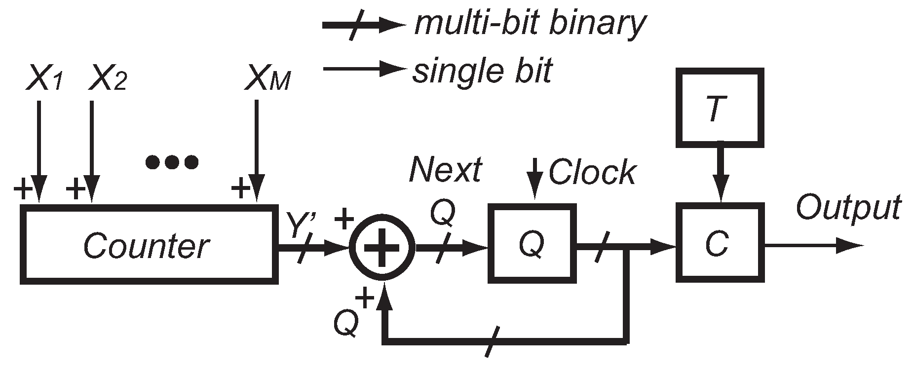
M is an arbitrary positive integer. In each clock cycle, the sum adder uses the counter in Equation (
3) to count all of the input bits and obtains the result in a signed binary format. Besides the current result in the counter, the adder also needs to consider the previous value of the counter. An adder adds the previous value, which is stored in memory, to the current counter value. If the added result is positive (negative), then the sum output is one bit
P (
N). If the added result is greater than +1 or less than −1, then the added result is updated and stored in memory for the next clock cycle. The value stored in memory has the same polarity of the added result, but its absolute value is reduced by one from the added result. This is because the output takes one bit from the value. If the added result is zero, then the stored value is zero, and the output takes one bit from a toggling signal. This is because a toggling bit-stream has an analog value of zero, so adding toggling bits does not affect the analog value of the sum bit-stream.
A simplified schematic of a Delta Sigma sum adder is shown in
Figure 6.
X to
X are Delta Sigma bit-streams as addends and inputs to a
Counter. The
Counter operates using Equation (
3) and generates a signed binary number
Y’.
Y’ is added to the value in
Q by a binary adder. Here,
Q is a register storing the previous results from the
Counter.
Q has the same number of bits as
Y’. The added result of
Y’ and
Q determines the output bit through
C. Here,
C is a digital comparator, whose output is one
P bit if the input binary number is above zero or
N if the input is less than zero. If the added result of
Y’ and
Q is zero, then the output takes the value from a toggling bit
T, and
T toggles for the next cycle,
i.e., T = NOT(T). If the added result of
Y’ and
Q is not zero, a new value of
Q is calculated and stored. The truth table of the circuit is summarized in
Table 2. To avoid overflow errors, when
Q reaches its maximum or minimum value, it should keep the value instead of rolling back to zero.
Figure 6.
Simplified schematic of the Delta Sigma sum adder.
Figure 6.
Simplified schematic of the Delta Sigma sum adder.
Table 2.
Truth table of the sum adder.
Table 2.
Truth table of the sum adder.
| Q + Y’ | ≥1 | ≤−1 | 0 |
|---|
| Next Q | Q + Y’ − 1 | Q + Y’ + 1 | 0 |
| Output | P | N | T |
| T | T | T | NOT(T) |
3.2. Delta Sigma Average Adder
Based on the Delta Sigma sum adder, we design the Delta Sigma average adder. The average adder generates an output Delta Sigma bit-stream, whose analog value is the average of all input Delta Sigma bit-streams. The average adder is essentially a digital Delta Sigma modulator, which can be realized in first-order or higher-order. The order number of the digital Delta Sigma modulator should be equal to or higher than the order number of the input bit-streams to maintain the signal-to-noise and distortion ratio (SNDR). For example, if the input bit-streams are generated by second-order Delta Sigma modulators, then the digital Delta Sigma modulator in the average adder should be at least second-order. Otherwise, the SNDR of the output bit-stream decreases from that of the input.
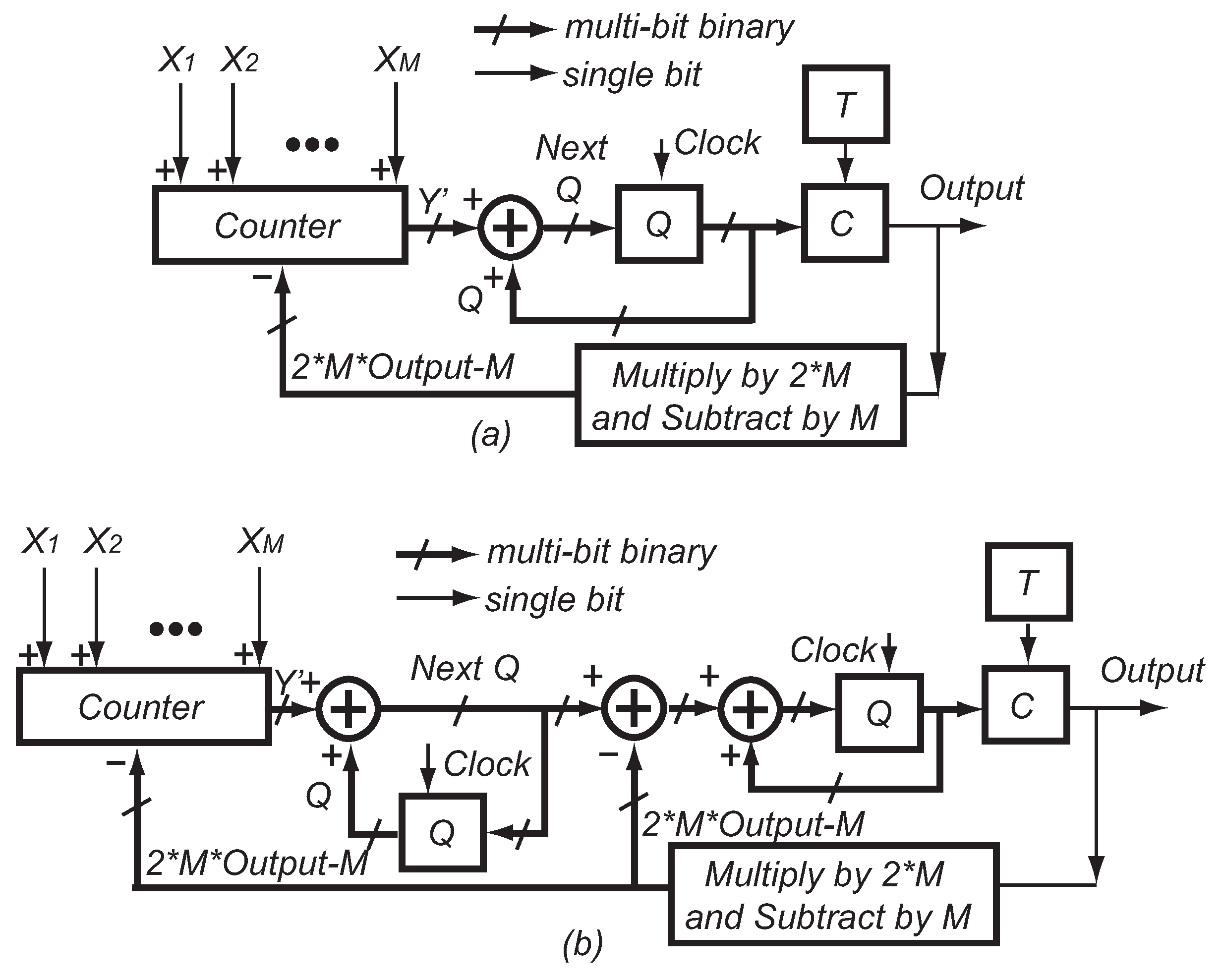
Simplified schematics of the Delta Sigma average adders are shown in
Figure 7.
Figure 7a shows a first-order average adder, which has a similar structure to the sum adder in
Figure 6. It also shares the same truth table with the sum adder. The difference is that the average adder has a feedback path from the output to the
Counter. The equation of the
Counter in an average adder is:
where
Output equals one (zero) if it is
P (
N). Thus, in each clock cycle, the input bits are added to the feedback bits from the output. The maximum value of feedback is the same as the sum of the maximum value of all input bits. The feedback bits are negated from the output bit,
i.e., every feedback bit is
P if the output bit is
N, or
vice versa. The added result of
Y’ and
Q determines the output bit and the next
Q according to
Table 2. We can also extend the first-order average adder to a second-order average adder, as shown in
Figure 7b.
Figure 7.
Simplified schematic of the Delta Sigma average adders. (a) First-order average adder; and (b) second-order average adder.
Figure 7.
Simplified schematic of the Delta Sigma average adders. (a) First-order average adder; and (b) second-order average adder.
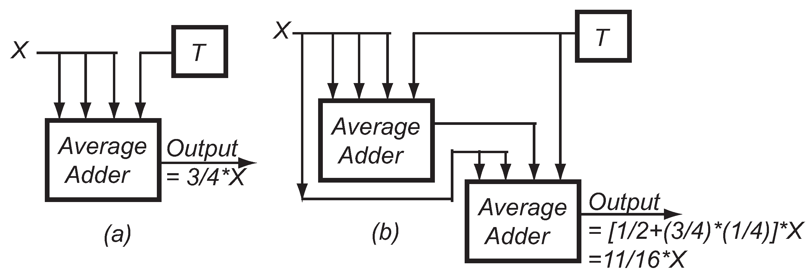
The average adder can also be used as a coefficient multiplier by a coefficient less than unity. The coefficient multiplier generates a new Delta Sigma bit-steam, whose analog value equals the analog value of the input bit-stream multiplied by a pre-defined coefficient. For example, the coefficient can be
m/
M, where both
m and
M are integers and
m is smaller than
M. This can be realized by using an
M-input average adder with
m of its inputs connected to the input bit-stream, while the other
M −
m inputs are connected to a toggling bit-stream, as shown in
Figure 8a, where
M = 4 and
m = 3. The toggling bit-stream, which has an analog value of zero, is running at the same bit rate of the input bit-stream. When a higher resolution of the coefficient is required, a cascade structure can be applied using more stages of average adders, as shown in
Figure 8b.
Figure 8.
Simplified schematic of the Delta Sigma coefficient multiplier based on the Delta Sigma average adder: (a) one stage; and (b) cascade structure.
Figure 8.
Simplified schematic of the Delta Sigma coefficient multiplier based on the Delta Sigma average adder: (a) one stage; and (b) cascade structure.
The proposed Delta Sigma adders have several advantages. First, they can take any number of input addend bit-streams compared to the two-input Delta Sigma adders in [
22]. Second, the circuit complexity and power consumption are lower than other Delta Sigma adders. This is because when adding more addends, it only requires a linear increase in the size of the counter and memory. Therefore, the complexity of the proposed Delta Sigma adder circuits of
N inputs is Θ(
N), which is better than Θ(
N) when circuits using sorting networks are applied [
13]. Furthermore, compared to multi-bit binary adders, the proposed Delta Sigma adder can take addends at different clock rates, as long as the adder clock is equal to or faster than the highest clock rate among all addends.
4. Simulation of Delta Sigma Adders
This section presents simulation results of the Delta Sigma sum adder and the average adder. We simulated the proposed sum adder and the average adder in MATLAB using the Delta Sigma Toolbox [
34].
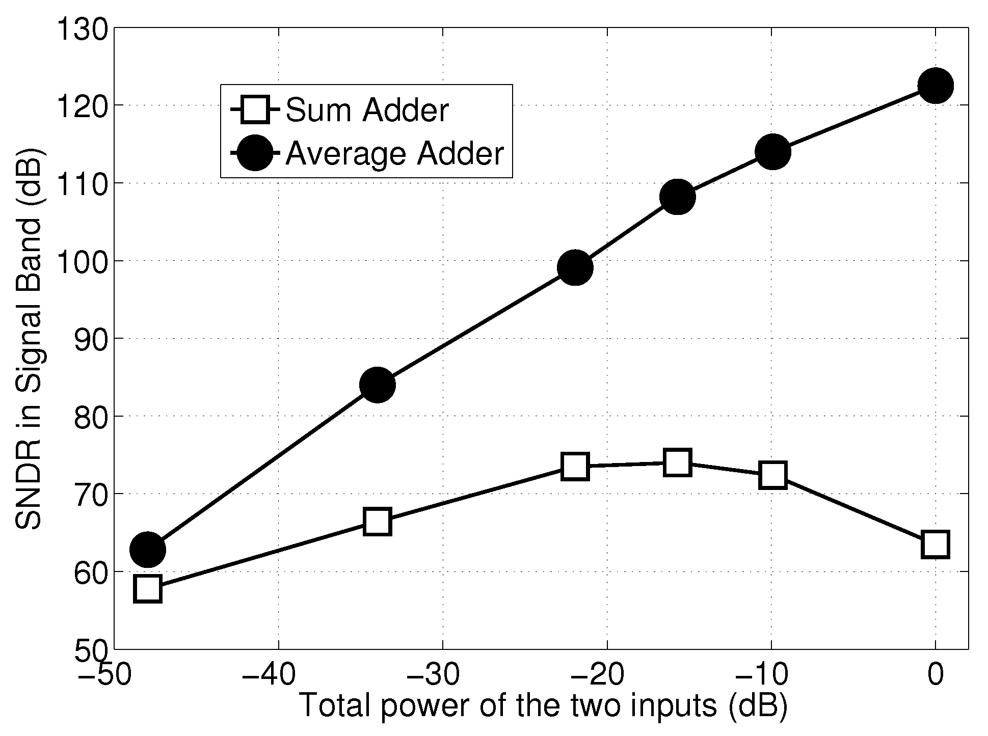
Figure 9 shows the simulated SNDR plotted against the input power of a two-input average adder and a two-input sum adder both at an oversampling ratio (OSR) = 1024, where the inputs are Delta Sigma-modulated sine waves. Because the sum adder does not have feedback, the previous value
Q representing the “temporal overflow” bits may not be able to be completely assimilated by the output bit-stream. The temporal overflow remains in the system until the input bit-stream changes the polarity of its analog value. Therefore, the temporal overflow can stay in the system for a long time and affects the output results. This process introduces extra noise in the output bit-stream. This noise increases when the input amplitude is high, because there are more “temporal overflow” bits at a higher amplitude. Furthermore, this noise increases with the number of addends. This is because when the number of addends is large, there are higher chances of having temporal overflow when input signals are in-phase.
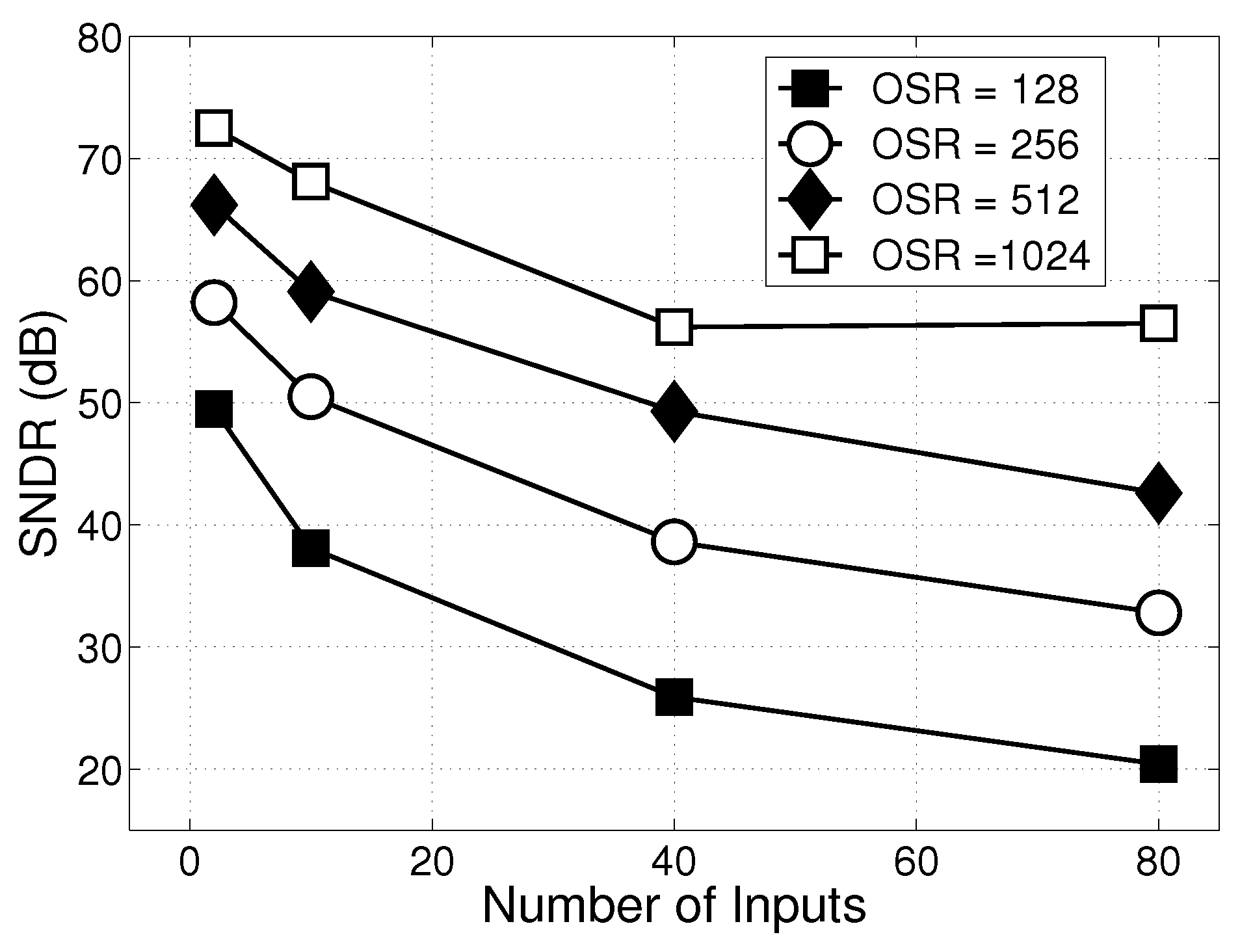
Figure 10 shows MATLAB-simulated SNDR as a function of OSR and the number of inputs in a Delta Sigma sum adder, where the input signals are sine waves modulated by second-order Delta Sigma modulators.
Figure 9.
Simulated output signal-to-noise and distortion ratio (SNDR) v.s. input power in a two-input sum adder and a two-input second-order average adder both with oversampling ratio (OSR) = 1024.
Figure 9.
Simulated output signal-to-noise and distortion ratio (SNDR) v.s. input power in a two-input sum adder and a two-input second-order average adder both with oversampling ratio (OSR) = 1024.
Figure 10.
Simulated output SNDR in a Delta Sigma sum adder at different numbers of inputs and OSR.
Figure 10.
Simulated output SNDR in a Delta Sigma sum adder at different numbers of inputs and OSR.
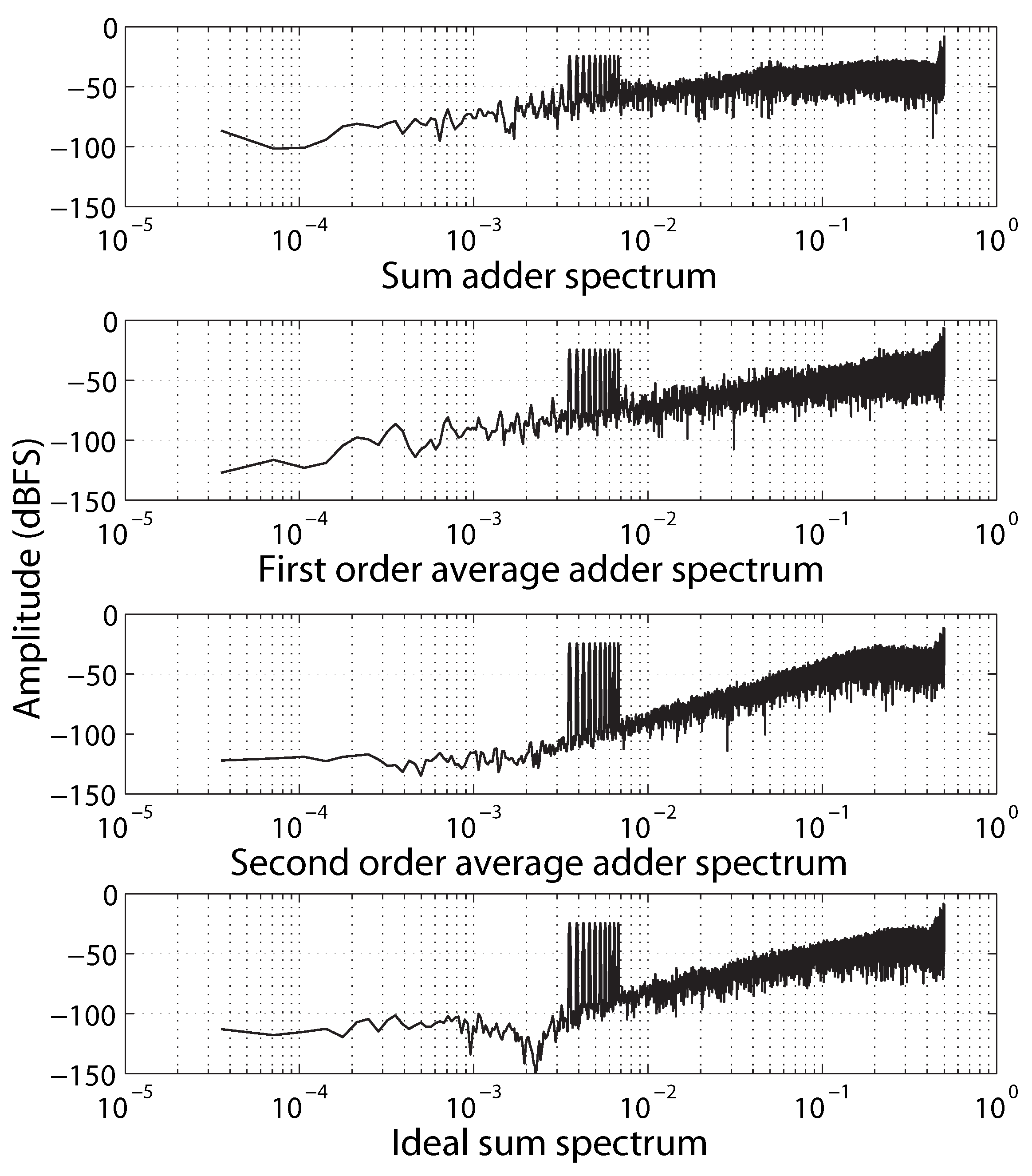
We simulated the output bit-stream spectrums of the sum and average adders, as shown in
Figure 11. Compared to the sum adder, the average adder has a feedback path that is able to completely merge its previous value with the current input bits within one clock cycle. Thus, there are no “temporal overflow” bits. Moreover, the feedback path enables the possibility of building higher-order digital Delta Sigma modulators that can further improve the noise shaping performance of the output bit-stream. In
Figure 11, we use ten sine waves with the same amplitude and different frequencies for the adders. The ten inputs are second-order bit-streams of sine waves with OSR = 1024. The frequencies are normalized to the sampling frequency of the Delta Sigma modulators.
Figure 11 shows that the noise floor of the sum adder is higher than the average adder by 50 dB. Furthermore, the noise shaping slopes in the sum adder and the first-order average adder are less than 30 dB/dec, while the output of the second-order average adder maintains a 40-dB/dec noise shaping slope, which is the same as the spectrum of the ideal second-order sum bit-stream.
Figure 11.
Simulated spectrums of Delta Sigma adders with ten addends.
Figure 11.
Simulated spectrums of Delta Sigma adders with ten addends.
In summary, while in a multi-bit binary DSP system, either a sum adder or an average adder can be used in digital filters, in a Delta Sigma DSP system, the average adder is preferred because of better noise performance.
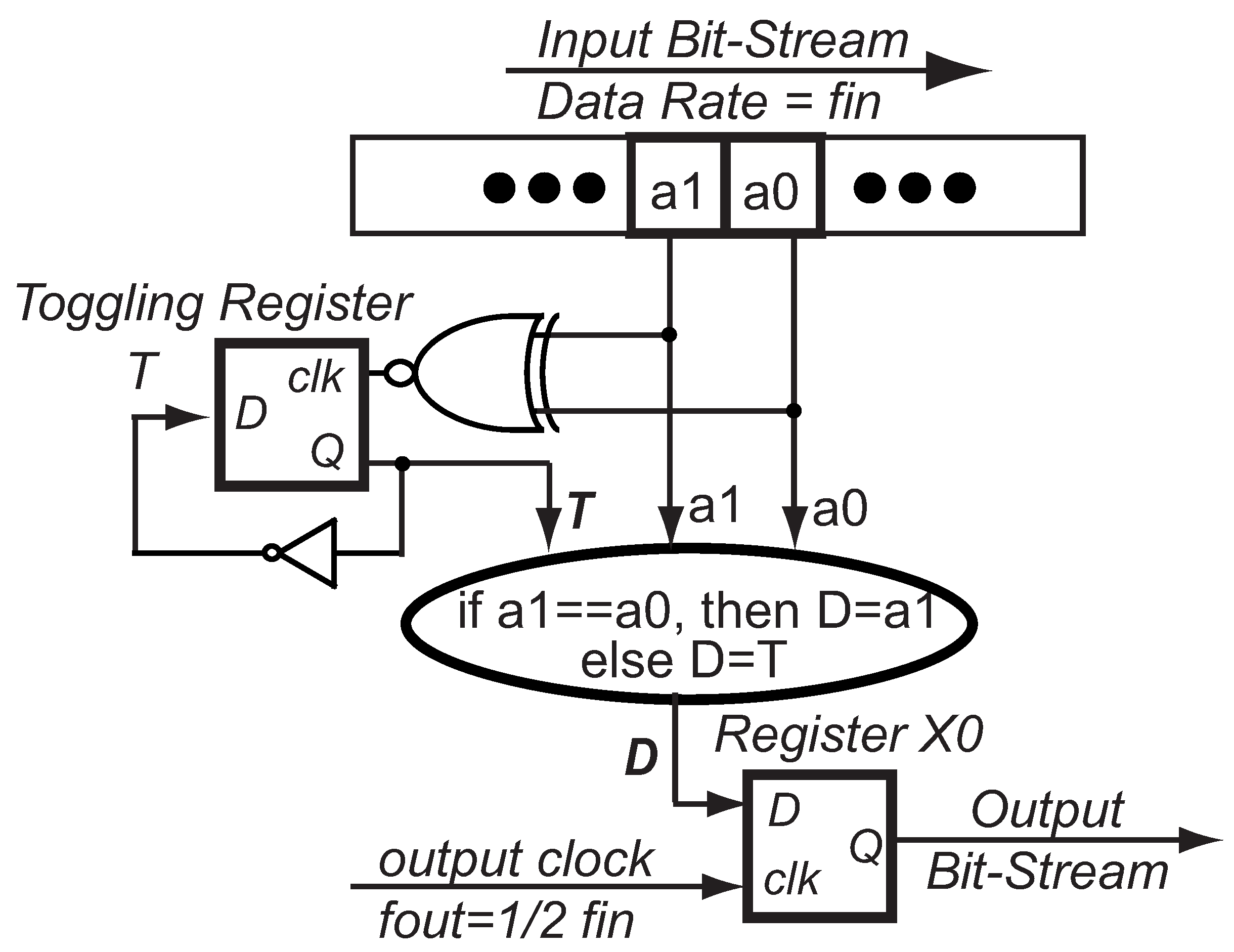
5. Downsampling and Delta Sigma Compressor
In this section, we discuss the techniques of changing the length of a Delta Sigma bit sequence while preserving its analog value. This is equivalent to adjusting the clock rate of a Delta Sigma bit-stream. We are particularly interested in downsampling a Delta Sigma bit-stream. However, we cannot simply use a lower speed clock to sample the Delta Sigma bit-stream and hope to preserve its analog value. Downsampling of a Delta Sigma bit-stream is equivalent to data compression. An algorithm is necessary to preserve the analog value while reducing the number of bits. Unlike complicated compressing algorithms in the multi-bit system, this work proposes a simple method based on Technique 3 in
Section 2. Essentially, we reduce the number of homogeneous bits and
P-N pairs with the same ratio, for instance
K. Then, the new bit sequence has the same analog value as the original bit sequence, and the length of the new bit sequence is 1/
K of the original bit sequence. This algorithm can be realized with simple circuitry using on-the-fly processing.
Here, we give an example of a Delta Sigma compressor circuit to reduce the data rate by 1/2. The circuit is shown in
Figure 12. Assume that a Delta Sigma bit-stream is coming into the compressor at a clock frequency
f. We use an
f/2 clock to sample two incoming bits at once. By doing so, any bit is only checked once in a two-bit window. We mark the two bits in the window as
a and
a, where
a is the preceding bit, while
a is the succeeding bit. If the two bits are homogenous, then the output bit
X should be the same polarity of the inputs. If the two incoming bits are heterogeneous, we take the value from a toggling bit
T as the output bit. The toggling bit
T toggles whenever the incoming two bits are heterogeneous. Thus, both the number of
P-N pairs and the number of homogeneous bits are reduced by 1/2 at the output. The value of
X at frequency
f/2 is the output Delta Sigma bit-stream. The Delta Sigma compressor can also be realized using the Delta Sigma average adder by adding sub-sequences from the original sequence, at the cost of increase of circuit complexity.
Figure 12.
Simplified circuit schematic of the Delta Sigma compressor.
Figure 12.
Simplified circuit schematic of the Delta Sigma compressor.
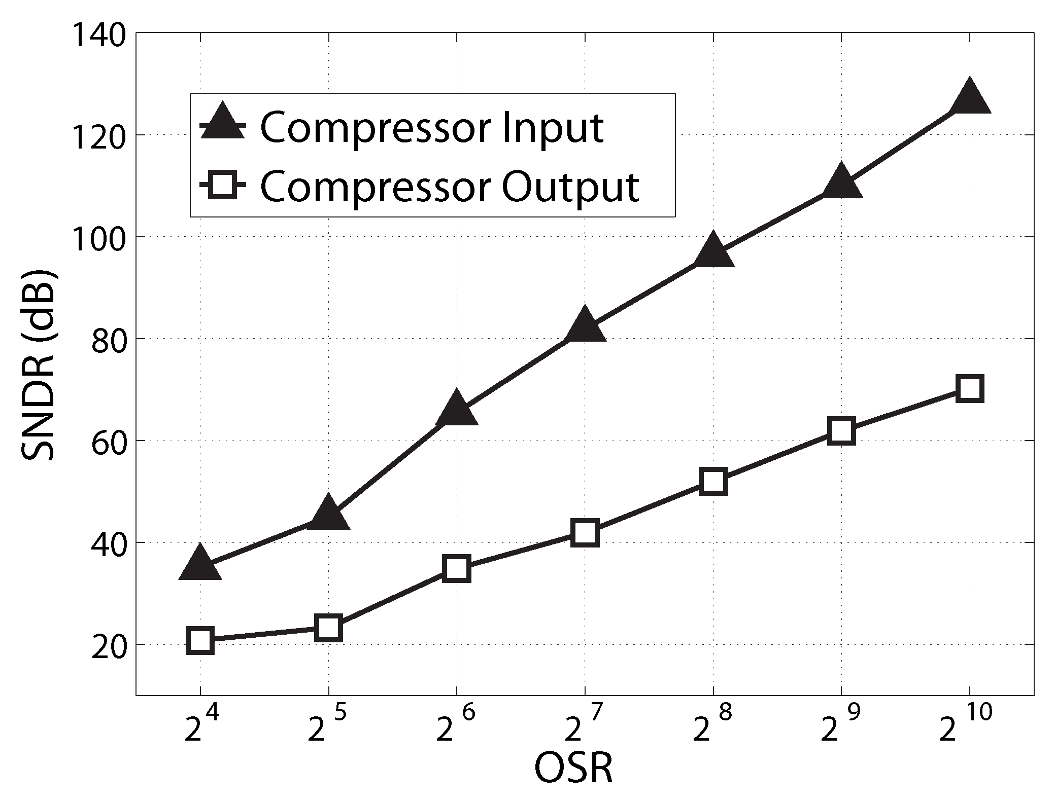
We simulated the SNDR of the compressor in MATLAB.
Figure 13 shows the SNDR of the input and output of the Delta Sigma compressor
versus OSR. The input is created by a second-order Delta Sigma modulator. Although the algorithm keeps the output analog value the same as the input analog value,
Figure 13 shows that the compressor reduces the SNDR because the OSR of the output bit-stream is half that of the input bit-stream.
Figure 14 shows the simulated input and output spectra of the Delta Sigma compressor with a second-order input bit-stream and OSR = 1024. The noise floor of the output spectrum increased by 50 dB compared to the input spectrum. Furthermore, the noise shaping slope of the output spectrum reduced to 20 dB/dec, which makes the output a first-order bit-stream. The compressor based on the first-order sum adder can only preserve the noise shaping of a first-order Delta Sigma bit-stream.
Figure 13.
Simulated signal-to-noise-ratio of the Delta Sigma compressor.
Figure 13.
Simulated signal-to-noise-ratio of the Delta Sigma compressor.
Figure 14.
Simulated input and output spectrum of the Delta Sigma compressor.
Figure 14.
Simulated input and output spectrum of the Delta Sigma compressor.
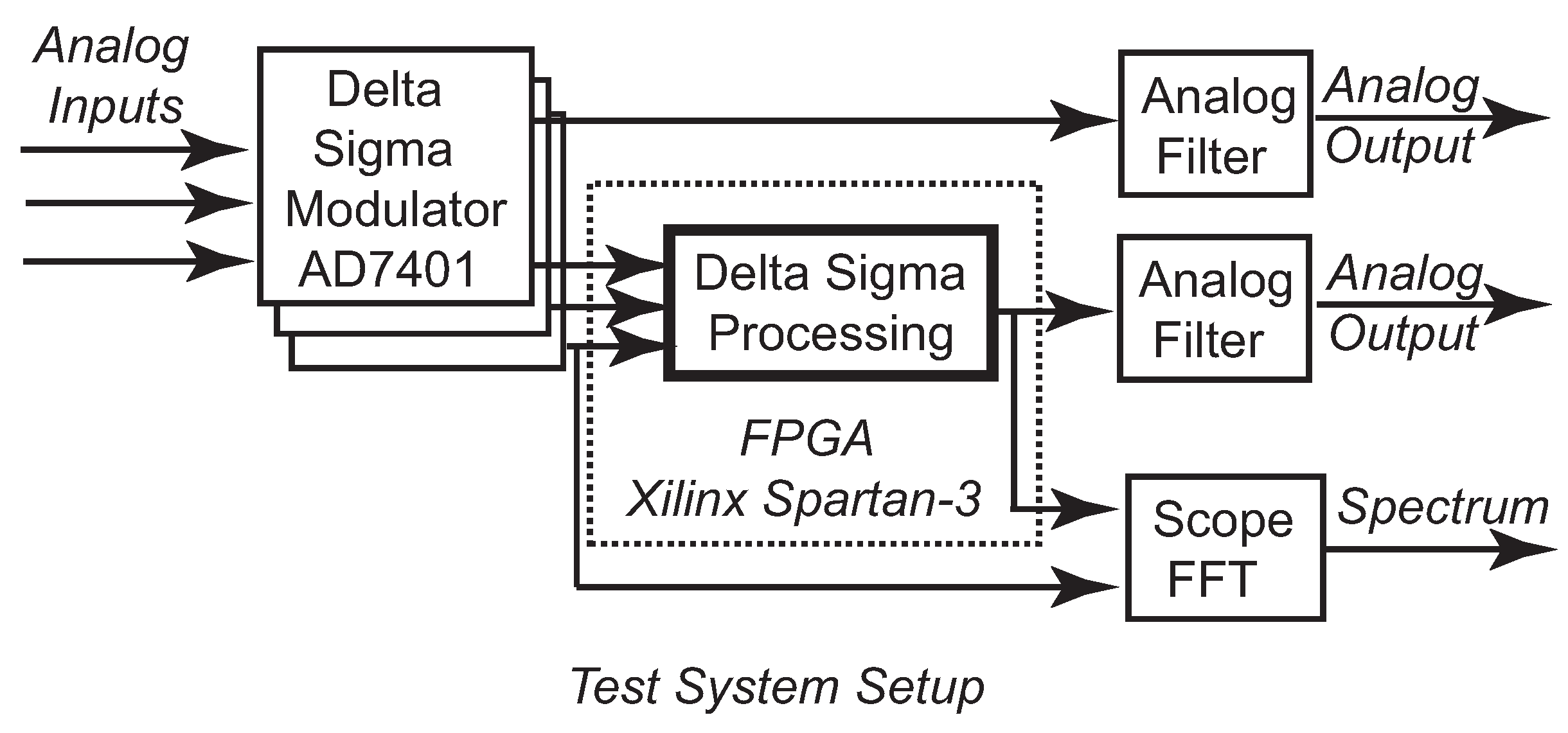
6. Measurement Results
We tested the proposed Delta Sigma signal processing circuits using a field programmable gate array (FPGA). The testbed is shown in
Figure 15. We used second-order Delta Sigma modulators AD7401 [
35] to generate the Delta Sigma bit-streams from analog signal generators. The Delta Sigma bit-streams are fed into the proposed Delta Sigma processing circuits, which include the sum adder and the average adder. The processing circuits are coded in Verilog and simulated by the Xilinx ISE isim simulator and then implemented on an Opal Kelly Spartan-3 FPGA board [
36]. In our experiment, an external function generator provided the clock signals to both the Delta Sigma modulator and the Delta Sigma processing circuit. Fourth-order analog filters recovered analog waveforms from both the Delta Sigma modulator and the Delta Sigma processing circuit. Oscilloscopes calculated the spectra of the digital signals using the FFT function. Both the AD7401’s output port and the Opal Kelly FPGA are powered by a 3.3-V power supply.
Figure 15.
Testbed setup for testing the Delta Sigma processing circuits.
Figure 15.
Testbed setup for testing the Delta Sigma processing circuits.
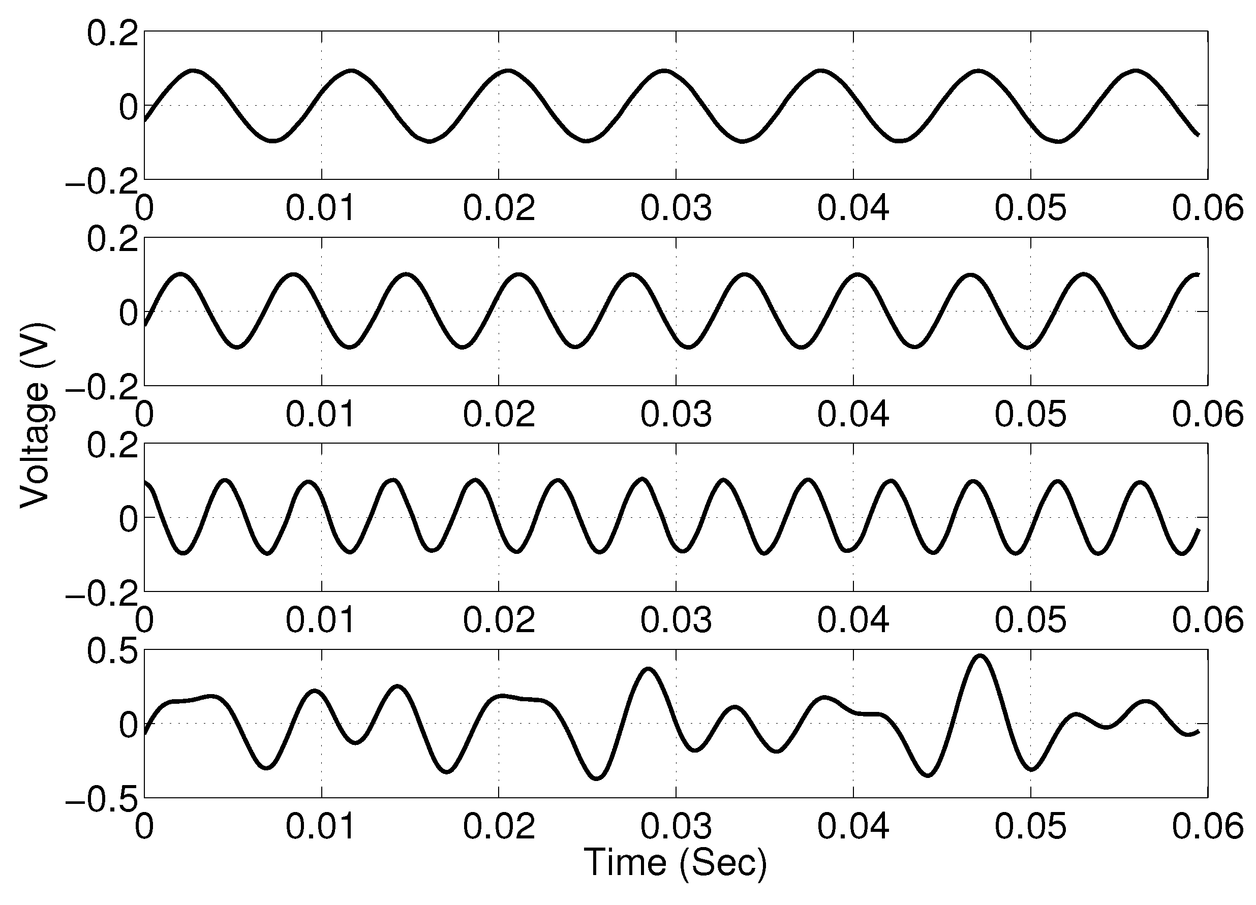
Figure 16 shows the input and output waveforms of a three-input second-order average adder. The three input signals are 113-Hz, 157-Hz and 213-Hz sine waves all with a 200-mVpp amplitude. The output waveform is recovered from a fourth-order analog filter. The output amplitude is higher than the amplitude of the inputs because of the internal gain of the AD7401.
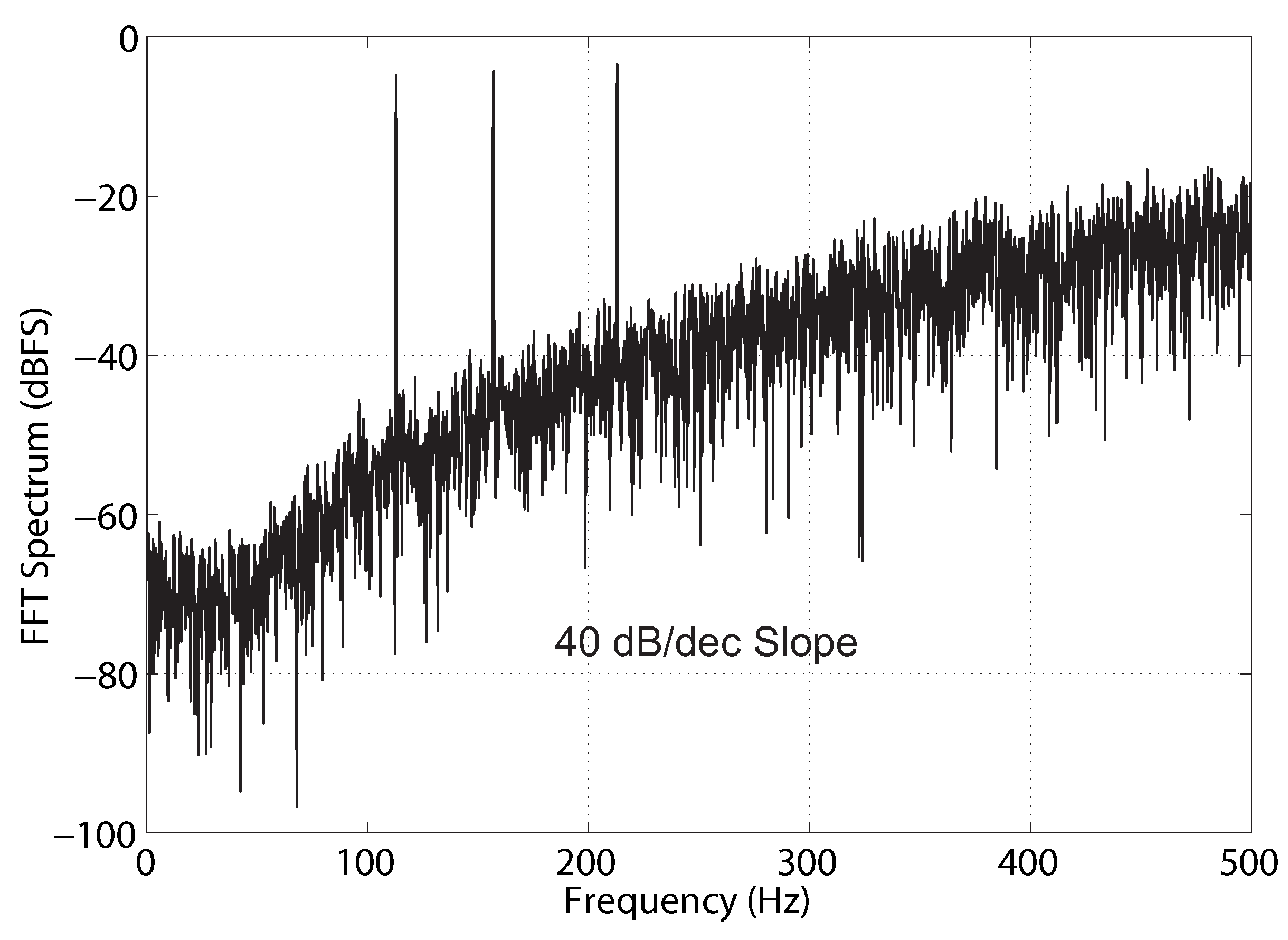
Figure 17 shows the FFT result of the second-order average adder output, which is calculated by the oscilloscope. In
Figure 16 and
Figure 17, the functionality of the three-input average adder is verified. Furthermore, the 40-dB/dec noise shaping slope in
Figure 17 shows that the processed signal is a second-order Delta Sigma bit-stream. In order to get a better view of the noise shaping slope, the OSR is set at approximately 100 for the three signals, which makes the sampling clock of the AD7401 and the clock of the Delta Sigma average adder both at 4 kHz.
Figure 16.
Measured time-domain waveforms of a three-input Delta Sigma second-order average adder recovered by analog filters. From top to bottom: Input 1, Input 2, Input 3 and output.
Figure 16.
Measured time-domain waveforms of a three-input Delta Sigma second-order average adder recovered by analog filters. From top to bottom: Input 1, Input 2, Input 3 and output.
Figure 17.
Measured FFT spectrum of the output of a three-input Delta Sigma second-order average adder. The noise shaping slope is 40 dB/dec.
Figure 17.
Measured FFT spectrum of the output of a three-input Delta Sigma second-order average adder. The noise shaping slope is 40 dB/dec.
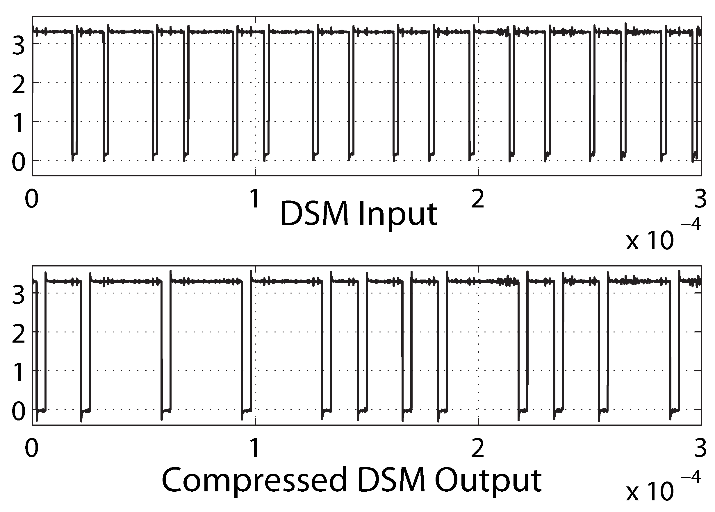
We also recorded the digital input and output waveforms of the Delta Sigma compressor, as shown in
Figure 18. In the test, we give a DC input of 500 mV and use a sampling rate of 500 kHz to obtain the input second-order Delta Sigma bit-stream. The output of the Delta Sigma compressor has half the data rate of the input Delta Sigma bit-stream. The input and output bit-streams have the same average duty cycle, which means the analog value of the input is preserved in the output.
Figure 18.
Measured time-domain input and output waveforms of the Delta Sigma compressor.
Figure 18.
Measured time-domain input and output waveforms of the Delta Sigma compressor.
7. Comparison between Delta Sigma Adders and Multi-Bit Adders
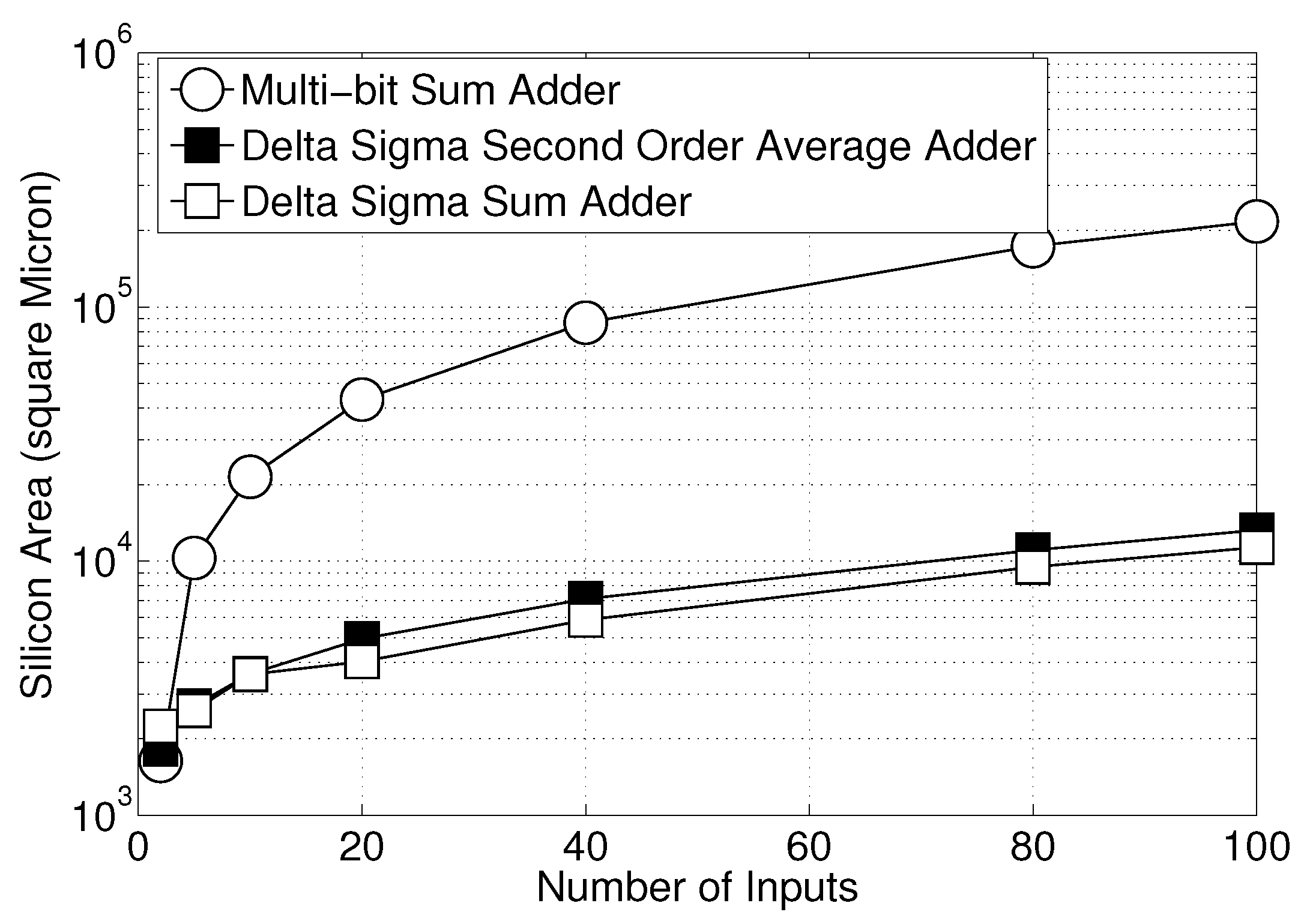
In linear DSP systems, higher-order FIR filters require adding many addends together at once. The proposed Delta Sigma processing circuits can significantly reduce circuit complexity compared to multi-bit processing circuits, especially when the number of inputs in an adder is large. In
Figure 19, we tested the integrated circuit area of the Delta Sigma sum adder, average adder and a multi-bit ripple-carry adder. The Delta Sigma sum adder has a simpler structure than the average adder. However, since the sum adder introduces extra noise, it is fair to compare the multi-bit binary adder and the Delta Sigma average adder, since neither circuit adds noise. We synthesized the Verilog code in the IBM 0.18-μm CMOS process using the Cadence RTL Compiler. The results show that if we replace the binary adder with the Delta Sigma average adder, the circuit area is reduced by 94% when the number of inputs is 100.
Figure 19.
Comparison of silicon area between the Delta Sigma adders and the binary adder.
Figure 19.
Comparison of silicon area between the Delta Sigma adders and the binary adder.
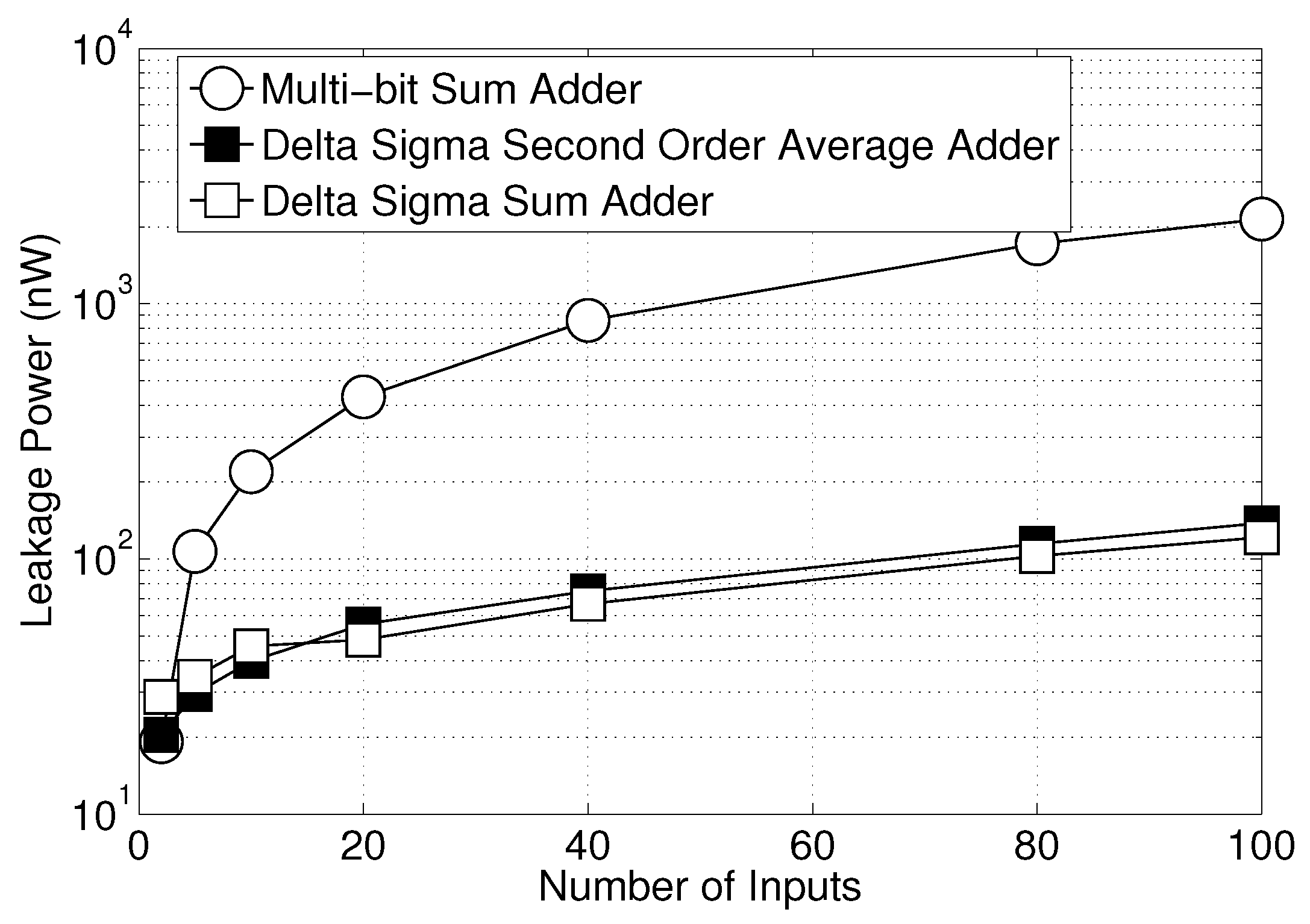
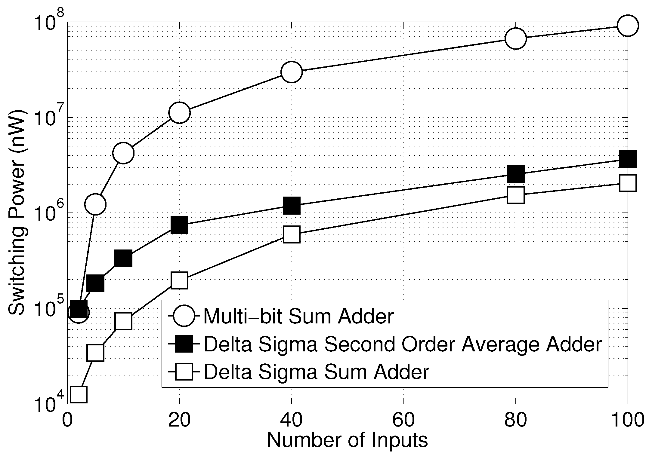
We also compared the power consumption between the proposed Delta Sigma adders and the multi-bit adder. In order to make a fair comparison, we refer to Texas Instruments ADS131E04 [
14]. It contains a Delta Sigma ADC made of a second-order Delta Sigma modulator, which operates at a fixed clock of 1024 kHz. The output sample rate of the ADC is 16 kSamples/s with 24-bit resolution. This means that, if we use the Delta Sigma modulator in the ADS131E04 as the ADC and make the Delta Sigma sampling rate 1024 kSamples/s, the result is equivalent to having a 24-bit binary ADC with a sampling rate of 16 kSamples/s. Thus, utilizing the same resolution and sampling rate of the ADC, when we design DSP circuits, it is fair to compare the power consumption of the proposed Delta Sigma average adder at a 1024-kHz clock rate to a 24-bit adder at a 16-kHz clock rate. We compared the power consumption for different numbers of inputs between the Delta Sigma adders and multi-bit binary adders. The comparison includes leakage power, net power and switching power, which are shown in
Figure 20,
Figure 21 and
Figure 22, respectively. For a 100-input adder, the proposed Delta Sigma average adder reduces the switching power by more than 96% compared to the multi-bit adder.
Figure 20.
Comparison of leakage power between the Delta Sigma adders and a binary adder.
Figure 20.
Comparison of leakage power between the Delta Sigma adders and a binary adder.
Figure 21.
Comparison of net power between the Delta Sigma adders and a binary adders.
Figure 21.
Comparison of net power between the Delta Sigma adders and a binary adders.
Figure 22.
Comparison of switching power between the Delta Sigma adders and a binary adder.
Figure 22.
Comparison of switching power between the Delta Sigma adders and a binary adder.


