Article

Architectural Techniques for Improving the Power Consumption of NoC-Based CMPs: A Case Study of Cache and Network Layer

by
Emmanuel Ofori-Attah
,
Washington Bhebhe
and
Michael Opoku Agyeman
*
Faculty of Arts, Science and Technology, University of Northampton, Northampton NN2 7AL, UK
*
Author to whom correspondence should be addressed.
J. Low Power Electron. Appl. 2017, 7(2), 14; https://doi.org/10.3390/jlpea7020014
Submission received: 31 January 2017 / Revised: 17 May 2017 / Accepted: 23 May 2017 / Published: 29 May 2017
(This article belongs to the Special Issue Emerging Network-on-Chip Architectures for Low Power Embedded Systems)

Abstract

:
The disparity between memory and CPU have been ameliorated by the introduction of Network-on-Chip-based Chip-Multiprocessors (NoC-based CMPS). However, power consumption continues to be an aggressive stumbling block halting the progress of technology. Miniaturized transistors invoke many-core integration at the cost of high power consumption caused by the components in NoC-based CMPs; particularly caches and routers. If NoC-based CMPs are to be standardised as the future of technology design, it is imperative that the power demands of its components are optimized. Much research effort has been put into finding techniques that can improve the power efficiency for both cache and router architectures. This work presents a survey of power-saving techniques for efficient NoC designs with a focus on the cache and router components, such as the buffer and crossbar. Nonetheless, the aim of this work is to compile a quick reference guide of power-saving techniques for engineers and researchers.

1. Introduction

Recent advances in multi-core and multi-threading technologies have seen a great growth in CPU processing power caused by the progression of smaller transistors in fabrication technologies [1]. This reduction in transistor size permits the integration of billions of transistors on a single chip to enhance the performance of System-on-Chip (SoC)-based applications. As this increase in core count continues to grow rapidly, communication between them becomes an essential requirement for future SoC design. The on-chip interconnect, which was primarily used to establish this communication, was the traditional bus-based system. However, bus-based architectures’ inability to cope and sustain this advancement in technology creates a performance bottleneck in the system. Therefore, the Network-on-Chip (NoC) paradigm has emerged as the integral backbone of emerging computer systems [2], thus shifting the focus of the development of technology to the enhancement of network performance. Unfortunately, this focus of improving network performance became such a predominant research area that very little emphasis was placed on the improvement of storage systems; which in effect caused a degradation in performance because of the storage systems incapability of handling this new growth in technology [3].
Nevertheless, over the last decade, the research community has made attempts to alleviate and bridge down the disparity between memory and performance by introducing Network-on-Chip-based Chip-Multiprocessors (NoC-based CMPs). Figure 1 depicts an image of a typical 2D NoC-based shared-memory chip multiprocessor comprised of 36 nodes. Each node consists of a core, private Level 1 instruction and data caches, a second level cache, which could either be shared or made private, a router and logic block. Connection is established between each node through the routers using links. Nonetheless, power consumption in NoC-based CMPs is proving to be a problem for SoC designers; particularly in the cache and the router. Furthermore, preliminary reports indicate that as this advent in technology and transistor size reduction continues, leakage power will be become a major contributor of NoC’s power consumption [4,5]. Routers consume a staggering amount of NoC power. Power-hungry components such as the input buffers and crossbars limit designers from maximising the capabilities of these systems. Continuous switching of activities results in high dynamic and leakage power consumption, thus causing a surge in the amount of power consumed on the chip.
Elsewhere, the recent advancements in video streaming, image processing and high speed wireless communication have immensely affected the design methodology for cache [6]. These advancements place demands for high performance and low power consumption in embedded systems. Objectives have shifted from achieving high peak performance to achieving power efficiency. Therefore, embedded systems present a challenge for designers because of their power and performance budgets.
NoC-based CMPs usually employ the two-level on-chip cache hierarchy: the private L1 cache and public L2 cache. The L2 cache is shared among resources because of its large capacity size and high association to provide fast access for resources [7,8]. However, due to the high utilization of these caches, they exhibit high switching power caused by the large amount of power consumed in the tag-comparison operation. In addition to this, more power is consumed because L2 caches require high associativity to reduce conflict misses, causing a large amount of power to be spent on tag-operations. Moreover, cache coherence for CMPs increases the power consumption in tag operations. Cache memory consumes a significant amount of the processor power, approximately 42% in swarm processor and 23% in Power PC [9].
Subsequently, it is not practically feasible to increase the cache size indefinitely. The increase in cache size can have a negative effect on the cache speed, hit rate, cache line size and the associativity for the applications. Hence, static and/or dynamic power consumption must be reduced without material performance degradation. Therefore, efficient techniques are required to balance network and power performance in both the caches and routers to minimise the surge in power. Particularly, to achieve this, we have investigated power-saving techniques for the cache and router in CMPs. The rest of the paper is organised as follows. Section 2 presents a literature review of the cache architecture, cache components and its distinctive designs to gain more understanding about the cache. Section 3 presents leakage power saving techniques for the cache, while Section 4 focuses of the dynamic power-saving techniques, as well as power-saving techniques that attempt to save both dynamic and leakage power in caches. Section 5 discusses efficient techniques for the buffers and crossbars regarding the NoC Layer, and finally, Section 6 concludes the paper.

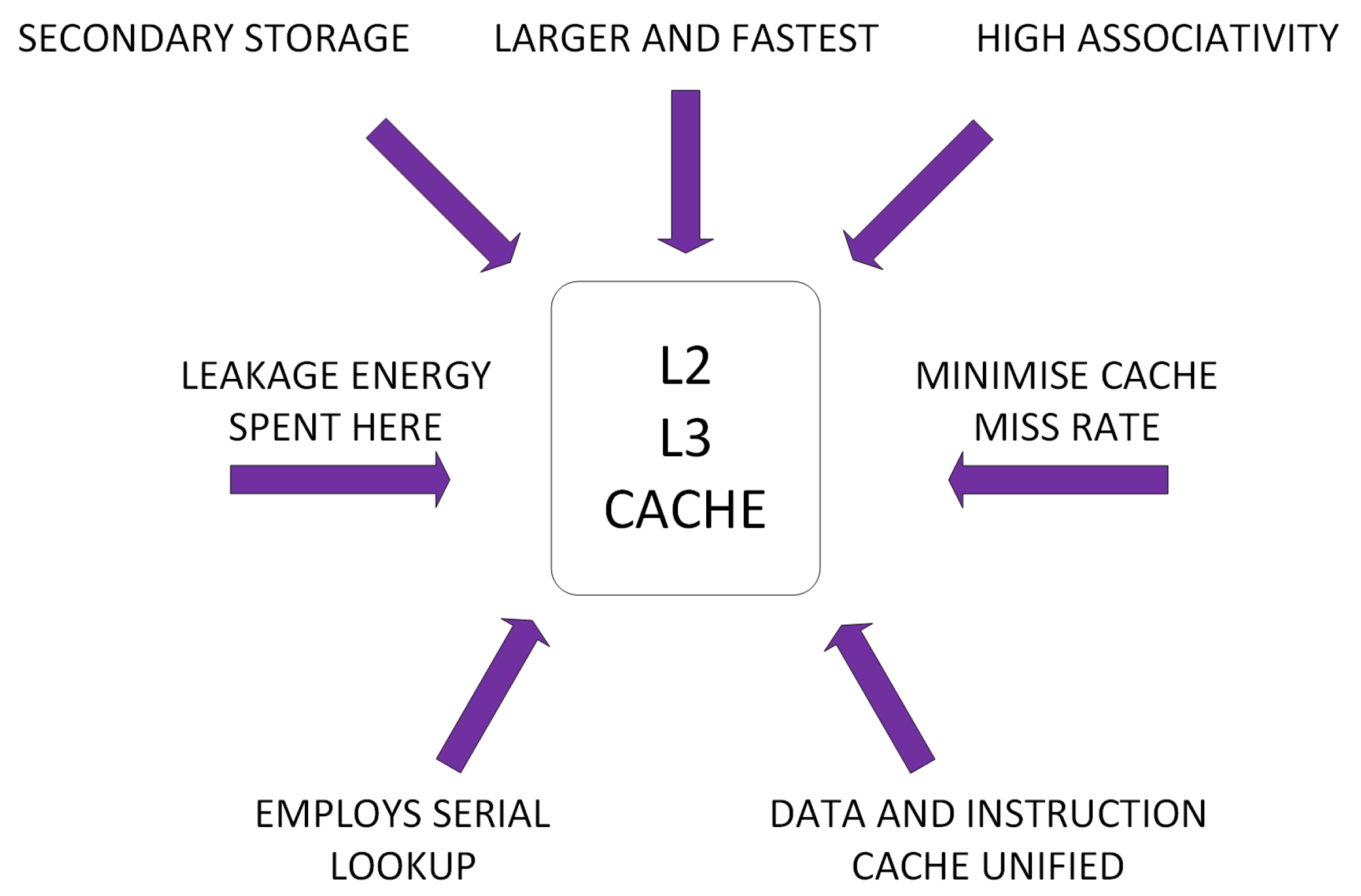
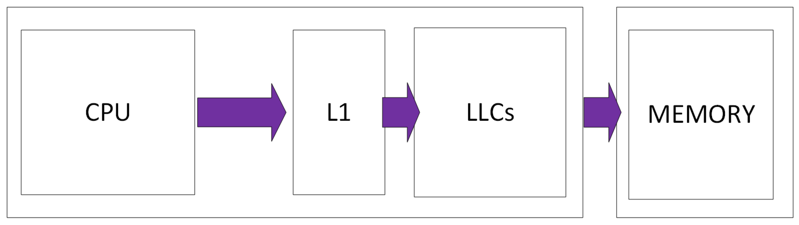
2. Cache: Power Concept, Architecture, Power Saving Chips (Engineering Approach to Power Saving)

This section of the paper presents the design methodology of the cache architecture with a view toward understanding how the cache is designed, the components of the cache and the several types of its organisation. The last section of the background focuses on how power is dissipated in the cache architecture, the different types of power consumption and in which parts in the cache they materialise.
The cache memory is a small, high speed memory, which is designed for Static RAM (SRAM) and consists of the most recently accessed data of the main memory. Due to their size, caches cannot store all of the code and data of an executing program. The cache memory is situated between the processor and the main memory Dynamic RAM (DRAM). Caches are known to perform 75% faster than their DRAM counterparts [10]. This is because it takes a shorter amount of time (15 ns) to retrieve information stored in the cache memory than the DRAM (60 ns). Moreover, the process of fetching an instruction from storage consumes time and power; therefore, to avoid the performance bottleneck at the input, the cache needs to be fast.
The memory design strictly centres on the principle of locality reference, meaning that at any given time, the processor accesses a small or localised region of memory. The cache loads this localised region. Internal 16 K byte cache of a Pentium processor contains over 90% of the addresses requested by the processor, making a hit rate of 90% [11]. It is not feasible to replace the main memory with SRAM to upgrade the performance because it is very expensive, less dense and consumes more power than DRAM. Therefore, increasing the amount of SRAM will have a negative effect on the performance since the processor will have more area to search, thus resulting in more time and dynamic power being spent on fetching. In addition, the cache needs to be of a size that the processor can quickly determine a hit or a miss to avoid performance degradation.
A cache architecture has two policies: read and write. The read architecture can either be a look aside or a look through; whereas the write policy architecture can be a write back or write through. A cache subsystem can be divided into three functional blocks: SRAM, Tag RAM (TRAM) and the cache controller. The SRAM is the memory block and contains the data. Relatively, the size of the SRAM memory block determines the size of the cache. The Tag RAM on the other hand is a small section of the SRAM, which stores the addresses of the data that are stored in the SRAM. The Cache Controller (CC) is identified as the main brain of the cache. It is responsible for the following actions: performance snoops and snarfs, implementing the write policy and updating the SRAM and TRAM. In addition to this, it is also responsible for determining if memory requests are cacheable and to also identify if a request has been a miss or hit.
Subsequently, caches consist of different organisations. These are Fully-Associative (FA), Direct Map (DM) and Set-Associative (SA). A cache is FA if a memory block can be mapped to any of its entries. FA permits any line in the main memory to be stored at any location in the cache. For this purpose, it is deemed to provide the best performance. In addition to this, it does not use the cache page, only the lines. The main disadvantage associated with FA is its high complexity during fetching. During this process, the current address is compared with all of the addresses in the TRAM. This process requires a very large number of comparators, thus increasing the complexity and cost of implementing large caches.
The DM, on the other hand, divides the main memory into cache pages. The size of each page is equal to the size of the cache. DM cache may only store a specific line of memory within the same line of cache. Although DM is the least complex and less expensive compared to the other organisations, it is far less flexible, making the performance much slower especially when moving between pages. Lastly, the SA cache scheme is a combination of FA and DM. Under SA, the SRAM is divided into equal sections called cache ways. The cache page is equal to the size of the cache way, which is treated like a small direct mapped cache.

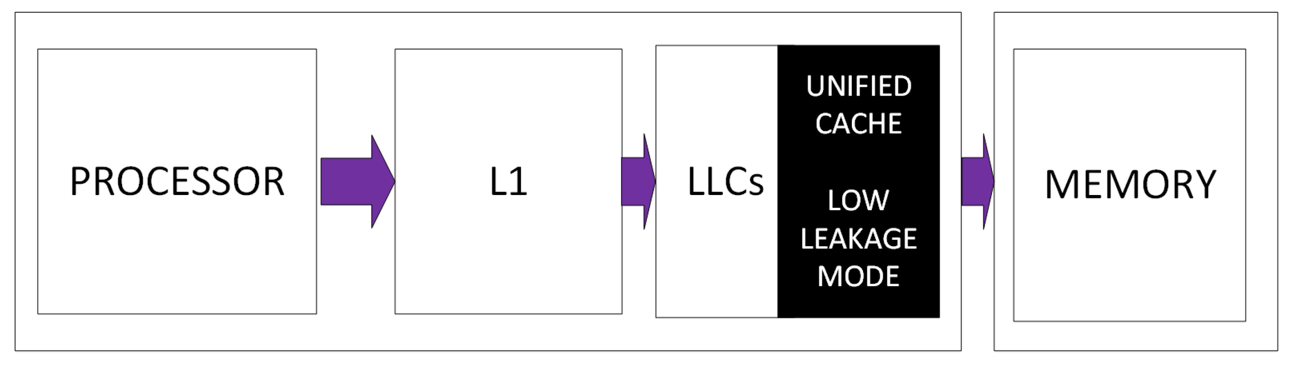
2.1. Cache Power Consumption

The power consumption of the Complementary Metal Oxide Semiconductor (CMOS) in CMPs is either dynamic power or leakage power (Figure 2). Dynamic power dissipation occurs in CMOS whenever transistors switch to change in a particular mode. This happens when the processor is either fetching for an instruction, reading or writing. Leakage power on the other hand occurs as a result of device inactivity or stand-by mode. The power consumption in the cache can be modelled by the dynamic and leakage:
P d y n a m i c = a × × C e f f × V D D
P l e a k a g e = V D D × I l e a k × N × k d e s i g n
where a is the activity factor, V D D is the supply voltage, C e f f is the effective capacitance, F refers to the operating frequency, N is the number of transistors, k d e s i g n is the design dependent parameter and I l e a k is the leakage current.
The architectural cache techniques designed to save power consumption seek to manipulate the two equations above [12]. The techniques with the objective of saving dynamic power do so by adjusting the voltage and frequency operation or by reducing the activity factor; whereas, the techniques aiming to reduce the leakage power consumption seek to re-design the circuit to use low power cells and also reduce the total number of transistors or by putting the unused parts of the cache into low or sleep leakage mode [13].

2.2. Cache Architecture

Figure 3 depicts the design methodology for a three-level cache architecture: L1, L2 and L3. The First-Level Cache (FLC) is the L1 cache. The L2 and L3 are called Lower Levels of Caches (LLCs). These caches contain unique properties. Over the years, several techniques have been proposed to effectively optimize these properties to reduce power consumption. The data and instruction caches are separated at the L1 cache, whereas L2 and L3 cache data and instructions are unified. By design, FLCs minimise access latency while LLCs minimise cache miss-rate and the number of off-chip accesses. FLCs are smaller by design and have smaller associativity and employ parallel lookup and tag arrays. LLCs, on the other hand, are much larger, have higher associativity and employ serial or phased lookup of data and tag arrays. As a result of their relatively smaller sizes and number of accesses, FLCs spend a larger fraction of their power in the form of dynamic power; while the LLCs spend a larger fraction of their power in the form of leakage power. Figure 4 and Figure 5 summarize the nature of FLCs and LLCs.
Mittal et al. [12] conducted a similar survey of architectural techniques on saving power in cache in 2012. However, this work differs from their work because in this fast-growing and evolving area, many techniques have been proposed since 2012. Hence, this work complements his work by focussing on the developments that have taken place between 2013 and 2017. In addition, we present low power design techniques in routers at the buffer and crossbar level.

2.3. Power-Saving Chips

This section presents a survey of the most recent commercial chips designed to save power in the cache architectures. Warnock et al. [14] present the circuit and physical design of the zEnterprise EC12 Microprocessor chip and multi-chip module. This is a Processor Chip (CP), Level-4 cache chip and the multi-chip module at the heart of the EC12 system. The chips were implemented in IBM’s high performance 32-nm high-k/metal-gate Silicon on insulator (SOI) technology. The chip is designed to contain six super-scalars, out-of-order processor cores, running at 5.5 GHz, while the aforementioned chip contains 192 MB of embedded DRAM (eDRAM) cache. Six CP chips and two Level-4 cache chips are mounted on a high-performance glass-ceramic substrate providing high-bandwidth and low latency interconnections. The experimental result in [14] show that the EC12 Microprocessor chip provides an unprecedented level of system performance improvement. The introduction of the eDRAM in the cache introduces density, resulting in low leakage consumption.
Shum et al. [15] presented an IBM zNext chip, which is a third generation high frequency microprocessor chip. The chip has six cores instead of four, dedicated-core processors and a 48-MB eDRAM on-chip shared L3. The IBM zNext chip maximizes the out-of-order window because of its improved dispatch grouping efficiencies, which are the reduced cracked instruction overhead, increased branches per group and added instruction queue for re-clumping. zNext also has the capability of accelerating specific functions because of its short-circuit executions, dedicated fixed-point divide engine resulting in 25 to 65% faster operations and millicode operations. Haupt et al. [16] presented a heat transfer modelling of a dual-side cooled microprocessor chip stack with embedded micro-channels. This cooling approach is also called dual-side liquid cooling where the heat removal from the chip stack is enhanced by placing a liquid cooled interposer and thus dissipates heat from the stacked dies. This design achieves hydraulic diameters as large a 200 μ m.
Warnock et al. [17] describes a technique called the 5.5-GHz System zMicroprocessor and multi-chip module. This chip features a high-frequency processor core for running at 5.5 GHz in a 32-nm high-k CMOS technology using 15 levels of metal. This chip is an upgrade of the 45-nm chip with significant improvements made to the core and nest in order to increase the performance and throughput of the design. The 32-nm chip is capable of achieving a higher operating frequency while running at lower operating voltages than the 45-nm one. Fischer et al. [9] discussed a performance enhancement for 14-nm high volume manufacturing microprocessor and system on-chip processes. This is a performance enhancement to Intel’s 14-nm high-performance logic technology interconnects. The enhancements are the improved RC performance and intrinsic capacitance for back end metal layers over a range of process versions and metal stacks offered for optimal cost and density targeted for various applications. These enhancements were implemented without any reduction in reliability performance. Choe at al. [18] presented a sub- μ w on-chip oscillator for fully-integrated SoC designs. This oscillator introduces a resistive frequency locked loop topology for accurate clock generation; a switched-capacitor from the topology. The oscillator is then matched to a temperature-compensated on-chip resistor using an ultra-low power amplifier. A test chip is fabricated in 0.18- μ m CMOS that exhibits a temperature sufficient of 34.3 ppm/degrees Celsius with long-term stability of less than 7 ppm.
Yen et al. [19] presented a low store energy and robust Resistive random-access memory (ReRAM)-based flip-flop for normally-off microprocessors. The technique of normally-off computing benefits microsystems with a long sleep time. The normally-off computing system can turn off power to achieve zero power consumption and can activate microsystems instantly. This work is a novel ReRAM-based Non-Volatile Flip-Flop (NVFF), fabricated using 90-nm CMOS technology and the ReRAM process of the Industrial Research Institute. This ReRAM-based NVFF is able to reduce store energy by 36.4%, restore time by 64.2% and circuit area by 42.8% compared with the state of the art complimentary design. The ReRAM-based NVFF is also superior in reducing restoration error by 9.44% under hardship condition compared to NVFF with a single NV device.
Andersen et al. [20] introduced a 10 W on-chip Switched Capacitor Voltage Regulator (SCUR) with feed-forward regulation capability for granular microprocessor power delivery. SCUR is designed and implemented in a 32-nm SOI CMOS technology. The semi-conductor technology features the high capacitance density and low loss deep trench capacitor resulting in high efficiency and high power density on-chip designs. The implemented on-chip switched capacitor voltage regulator provides a 0.7 V to 1.1 V output voltage from 1.8 V input. It achieves 85.1% maximum efficiency at 3.2 W/nmm power density. The overall power consumption of the microprocessor can be reduced by 7%.

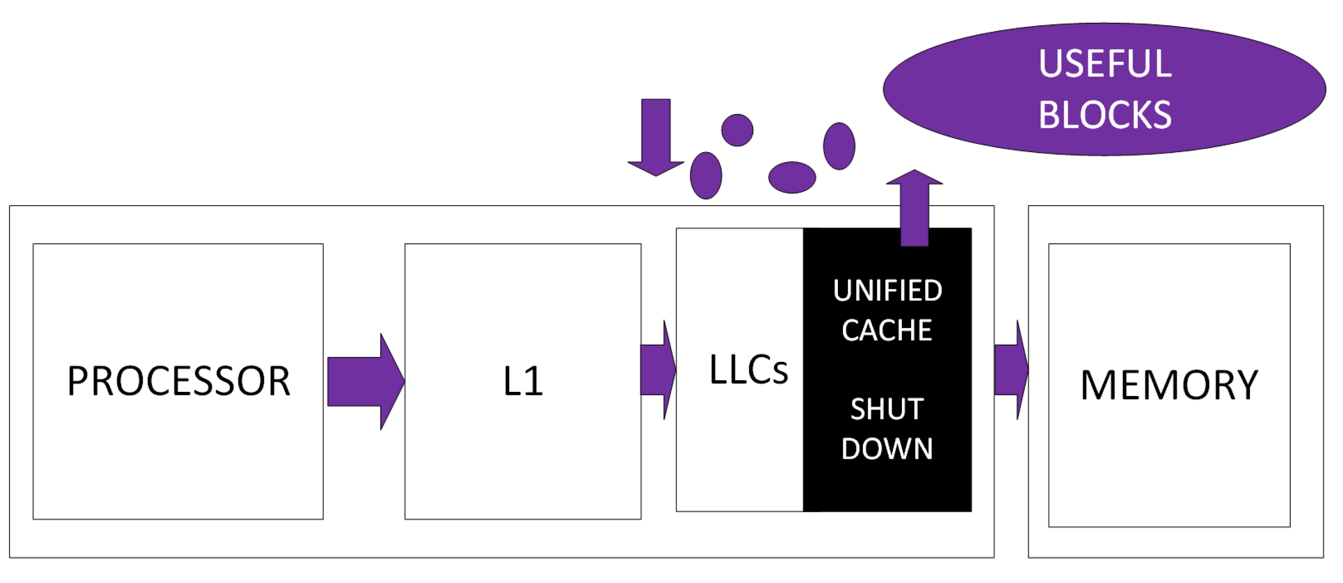
3. On the Leakage Power Saving Approaches in Cache Design

3.1. Concepts

Leakage power mostly materialises in the LLCs. Consequently, most existing work in the literature focus on disabling the idle parts of the cache or introducing DRAM, which is denser and does not suffer extensively from leakage power consumption. These techniques estimate the required size of the cache needed by a program before it runs and then turns off any unneeded cache space. Leakage power saving techniques are either state-destroying or state-preserving techniques. State-preserving techniques turn off the unneeded cache area and still preserve its state. When the cache space is re-activated, fetching the lower levels of memory is not needed. State-destroying techniques on the other hand do not preserve the state of the switched off cache space. If the destroyed cache space is required later, it has to be fetched in the lower levels of memory. The state-destroying techniques generally save more power than the state-preserving techniques for as long as the destroyed cache space is not needed. When the destroyed cache space is later needed, more power is spent in searching the lower level caches. Subsequently, various techniques that have been proposed to save leakage power share some of sort of similarities and are discussed below. Various researchers employ the Drowsy Cache Technique (DCT) to save the leakage power [21] as shown in Figure 6.
The DCT migrates a portion of unneeded cache into a low-leakage mode, thus saving power at the granularity level. Some researchers use the immediate sleep technique to turn off the unused cache [19,20,22]. Reconfigurable cache techniques are used to estimate the program miss-rate in an online manner [12,23,24,25,26].
Some techniques use power gating to migrate blocks deemed useful to a live partition before shutting down the unused cache [20,27] as shown in Figure 7. Some techniques focus on hybridisation of Phase-Change Random Access Memory (PCRAM) and DRAM to introduce a bit of density to the PCRAM and cause less leakage consumption [28].

3.2. Techniques

Many cache power saving techniques exist in the literature. These techniques can be divided into two groups: offline and online profiling. Offline profiling techniques execute workloads offline for application characteristics such as cache miss ratios in different cache configuration [29]. Consequently, offline techniques reduce the large overhead that occurs in online profiling systems. Online profiling on the other hand determines the best thread-to-core assignment during execution [29]. This section of the paper contains a classification of leakage power saving techniques for offline and online systems.

3.2.1. Offline Profiling

Cheng et al. [28] proposed an adaptive page allocation of DRAM/PCRAM hybrid memory architecture. This is a hybrid of DRAM and PCRAM, taking advantage of both components, reducing leakage energy. The technique uses DRAM as the last level of cache and PCRAM as the main memory. When the data stored in the DRAM block are not accessed for a period of time, it is ignored, and the refresh operation of the DRAM block is stopped. When the data accesses are found necessary after it has been ignored, the data are reloaded from the PCRAM. The technique uses a small DRAM as the cache of PCRAM memory to reduce leakage power consumption together with an adaptive page allocation scheme that is used to make better utilisation of the DRAM capacity. This results in the conflict misses of DRAM being minimised under the multi-core architecture. The architecture reduces the number of write backs to PCRAM, and data migration between PCRAM and DRAM is materially reduced. The results of the simulation show that both the power consumption and access latency of PCRAM is reduced by 25%.
Mittal et al. [25] proposed a technique called Cache Energy Saving Technique for Quality-of-Service systems (CASHIER). This technique uses a reconfigurable cache emulator that estimates the program miss-rate for various cache reconfigurations in an online manner. CPI stakes are used to estimate program execution time under different lower level cache configurations. The Energy Saving Algorithm (ESA) then uses the estimates to determine the memory sub-system energy under different cache configurations. From the results of ESA, a suitable cache is chosen that will strike the best balance between energy saving and performance loss, thereby avoiding a deadline. CASHIER saves on average 23.6% energy in memory sub-systems for a 2-MB L2 cache with a 5% performance slack allowed.
Bardine et al. [30] evaluated leakage reduction alternatives for a deep submicron dynamic non-uniform cache architecture. The results of the simulation show that cache decay has leakage savings and performance degradation comparable with way adaptable on Dynamic Non-Uniform Cache Architecture (D-NUCA). The drowsy cache is potentially able to get higher power reduction with some reduced performance losses.
Zhu et al. [31] used a triple-threshold-voltage nine-transistor SRAM cell technique for data stability and energy efficiency at ultra-low power supply voltages. The technique scales the power supply voltage V D D to enhance the integrated circuits efficiency. However, this efficiency causes a substantial degradation of reliability due to less noise margins of the CMOS circuits.
Cheng et al. [32] discusses a technique called ‘LAP’, which exploits energy-efficient asymmetric last level caches. The technique is designed to improve the efficiency of non-volatile memory-based LLCs, especially the redesign of inclusion properties and associated replacement policies to explicitly include write reductions. The technique also incorporates advantages from both non-inclusive and exclusive designs to selectively cache only part of upper-level data in the LLC. The simulation results show that the architecture out-performs other variants of selective inclusion and consumes 20% and 12% less energy than non-inclusive and exclusive Spin-Transfer Torque Magnetic Random-Access Memory (STT-RAM or STT-MRAM)-based LLCs.
Hameed et al. [33] proposed two-row buffer bypass policies and an alternative row buffer organisation to reduce the number of row buffers in STT-RAM-based last-level cache architectures. The experiments show that energy consumption is reduced by 19.5% compared to SRAM alone.
Hammed et al. [33] proposed a technique for architecting STT LLCs for performance and energy improvement. The technique uses a large chip of DRAM memory as LLC. The experiments show that on-chip DRAM LLC provides significantly improved performance benefits compared to an SRAM-based LLC with a high cache capacity. The technique employs STT-RAM as a larger LLC because of its low leakage, non-existent refreshing energy and its scalability benefits.
Khartan et al. [21] proposed a hardware-based approach for saving cache power in multi-core simulation of power systems. In this technique, the time domain simulation of power system is conducted and traces of analysis instructions recorded. The recorded traces are used in multi-core configurations. The Drowsy Cache Technique (DCT) is used as a cache leakage power-saving technique. DCT transitions a portion of cache into a low-leakage mode, thus saving the power cache granularity level. The results of simulations show an effective savings, keeping performance losses at a minimum. For a 2-MB two-core system, DCT saves 54% cache power, and for a 4-MB four-core system, up to 50.2% cache power is saved.
Rossi et al. [34] introduced Bias Temperature Instability (BTI) and leakage-aware Dynamic Voltage Scaling (DVS) for reliable low cache memories. The technique shows that the BTI-induced degradation greatly benefits leakage power saving of drowsy cache memories. The simulation results show that the leakage power can be reduced by more than 35% during the first month of use, more than 48% during the first year and up to 61% in ten years of memory operation. This shows that older memories give an opportunity of saving more leakage energy.
Bengueddach et al. [23] proposed a technique for energy consumption reconfiguration in two-level caches. The technique uses the dynamic reconfiguration approach in the multiprocessors. This memory hierarchy contribute largely to the energy consumption of the overall hardware/software architecture.
Mittal et al. [24] proposed a Flexi way, which is a cache energy-saving technique using a fine-grained cache reconfiguration-based approach for saving leakage energy. Flexi works on the observations that access to the cache sets are not distributed uniformly, making some sets seeing more accesses than others. The other observation is that of the difference in the associativity of sets. A cache is subdivided into small modules called subways. The selective-ways technique is used to turn off exactly the same number of ways for all of the modules, providing the fine-grained reconfiguration with caches of similar associativity, thereby avoiding the need to use caches of large associativity for fine-grained reconfiguration. The simulation results show that Flexi can achieve energy savings of 26.2% in dual core systems.

3.2.2. Online Profiling

Mittal et al. [12] present a multi-core power-saving technique using dynamic cache reconfiguration called A Multicore Cache Energy-Saving Technique Using Dynamic Cache Reconfiguration (MASTER) . MASTER uses a cache colouring scheme, allocating cache at the granularity of a single cache colour. This technique works by periodically allocating the required amount of LLC space to each running application and turns off unused cache space to save power. A reconfigurable cache emulator is used for profiling the behaviour of running programs under different LLC sizes. The energy-saving algorithm is used to predict the memory subsystem energy of running programs for a small number of colour values. MASTER uses these estimates to select a configuration with minimum estimated power and turns off the unused LLC to save leakage power. The V D D gate is also used by MASTER to implement the hardware of the cache block. The simulation results show that the average savings in memory subsystem energy over shared baseline LLC are 15% and 11%.
Kadjo et al. [27] proposed a novel power gating technique for LLCs in a chip multiprocessor. This technique greatly reduces the leakage power of LLC while reducing the impact on performance levels. High temporal locality blocks are migrated to facilitate power gating. The blocks expected to be used in the future are migrated from the block being shut down to a live partition at a negligible performance impact and hardware overhead. Simulations show that power savings of 66% can be reached at only 2.16% performance degradation.
Yue et al. [22] proposed a micro-architectural technique for run-time power gating in caches of the GPU for leakage power savings when they are idle during workload execution. The mode-transition latency is used to switch in and out of the low-leakage or sleep mode whenever needed. These latencies are micro-architecturally hidden to avoid performance degradation during workload execution. The low-leakage mode is state-retentive, meaning that it does not lose contents, and there is no need for flushing the caches after they wake up. Therefore, the L1 cache, which is private to the core, can be put into low-leakage sleep mode when there are no scheduled threads, and if there are no memory requests, the L2 cache can be put into sleep mode. This technique on average can save up to 54% of leakage energy.
Jing et al. [35] discuss the energy-efficient eDRAM-based on-chip storage architecture for General Purpose Graphics Processing Units (GPUPUs). The use of the eDRAM is proposed as an alternative for building an area and energy-efficient on-chip storage, including the RF, shared memory and L1 caches. eDRAM is chosen because it enables higher density and lower leakage power, but suffers from limited data retention time. To avoid periodic refreshing of the eDRAM, which makes performance suffer, lightweight compiler techniques are applied and runtime monitoring for selective refreshing that intelligently eliminates the unnecessary refreshes.
Charkrabotty et al. [36] used a technique called performance-constrained static energy reduction using way-sharing target banks. This technique improves the performance of the target banks by dynamically managing their associativity. The cost of the request is optimised by adding distance as another metric and thus reducing the performance degradation. Experiments show that static energy can be reduced by 43% and Energy-Delay Product (EDP) by 23% for a 4-MB LLC with a 3% performance constraint. The underutilised banks are powered off, and the requests re-mapped to target banks.
Wang et al. [26] propose a technique called system-wide leakage-aware energy minimisation using Dynamic Voltage Scaling (DVS) and cache reconfiguration in multi-tasking systems. DVS is integrated with Dynamic Cache Reconfiguration (DCR) techniques. The DVS and DCR make decisions judiciously so that the total amount of energy consumed is minimised. Using only the DVS or DCR in isolation leads to the wrong conclusions in the overall energy savings. This proposed technique is 47.6% more efficient than the leakage-aware DVS techniques and 23.5% than the leakage-oblivious DVS and DCR techniques.
Sampaio et al. [37] proposed a technique called the approximation-aware multi-level cells STT-RAM cache architecture. The aim of the technique is to achieve energy-efficient reliability optimisation in STT-RAM-based caches through what they called selective approximations of the storage data. The selective data approximation simplifies the error-protection hardware depending on the resilience levels and user-provided error tolerance of the applications. The technique aims at maximising the quality of the applications while minimising the energy consumption.
Kong et al. [38] proposed an energy-efficient PV-aware 3D LLC architecture. The technique exploits the narrow width values to save many faulty cache lines under severe process variation, which results in significant yield improvement in a highly energy-efficient manner with only a small performance loss and area overhead. The zeros are stored in the cache arrays with the faulty cache portions. A significant amount of leakage power is saved, which also contributes to the leakage-induced yield loss reduction.
Arima et al. [20] proposed a technique called immediate sleep for reducing energy impact of peripheral circuits in STT-MRAM caches. This technique aims to save the leakage power of peripheral circuits. Immediate sleep is also a power technique used for turning off a subarray of STT-MRAM caches immediately if the next access is not crucial or will not impede the performance levels. The technique uses power gating to STT-MRAM caches at the granularity of the subarray at runtime. The subarrays contain local decoders and write drivers. With every cache access, all of the decoders and write drivers are activated. Non-critical events are considered to be the write access and accesses, which arrive after a long interval. A next-access predictor algorithm is used to predict accesses for each subarray at runtime, and this prediction is made possible because there is a small number of subarrays in STT-MRAM LLCs. Shutting down these non-critical events subarrays can save a relatively large leakage energy without affecting performance. The immediate sleep technique has proven to save leakage power by 32% of an STT-MRAM LLC compared to the conventional scheme with STT-MRAM LLC.
Moreover, a summary of offline and online profiling techniques approaches has been presented. However, both of these techniques have their advantages and disadvantages. Online profiling is considered to supply better performance; however, techniques such as thread-swapping affects the performance, scalability and load balance of the system [39]. Offline profiling techniques, on the other hand, suffer to make an impact in running applications because of the complex and complicated program combinations [29]. In addition to this, since the dynamic workload of a system can change, the characteristics obtained from executing workloads can change during run-time. Furthermore, the techniques presented target different architectural levels. For example, the following techniques [12,20,21,22,23,24,26,27,28,32,33,34,35,37,40] target multi-core systems. Particularly, these target [20,27,32] CMPs. These techniques [30,31,38] are aimed at microprocessors.

4. On the Dynamic Power Saving Approaches in Cache Design

4.1. Concepts

Dynamic power techniques are normally applied in the FLCs because the majority of dynamic power materialises there. In the FLCs, the data and instructions are separate concerns unlike in the LLCs where they are unified. The techniques proposed for saving the dynamic power dissipation are not the same and are grouped below into how they seek to improve the consumption of dynamic power. Some techniques save dynamic power by employing a bloom filter, as shown in Figure 8 below.
The tag-bloom techniques use tags to directly map addresses in L1 and L2 caches [3,41,42]. The bloom filter algorithm is then used to predict the cache misses and divert the search to the main memory rather than to waste time and energy in searching the cache. Some techniques use the pre-fetching technique and cache locking to save dynamic power. The pre-fetching and locking techniques save power by reducing the penalty cost of cache misses. Some techniques aim to reduce the number of active ways accessed in each cache access to the number of ways halted in the case of a miss prediction using software or hardware. Other techniques reconfigure cache using computer software [43], while some techniques predict the program behaviour [3,41,42,44,45,46]. Some techniques deal with instructions in the cache [3,15,16,41,47,48,49,50,51,52]. Some techniques seek to leverage unused cache block words in order to reduce dynamic power consumption [18,36,53]. These techniques flush out the unused words from the cache and keep the cache current. Some techniques introduce a new level of cache called L0. L0 is placed between the processor and the L1 cache in order to improve the speed at which it can be accessed [44,54]. Some techniques use a near caching concept (Figure 9). The SRAM is placed closer to the memory rather than closer to the processor. This allows quick access of larger blocks from memory.

4.2. Techniques

Lee et al. [45] proposed a technique called filter data cache, which is an energy-efficient small L0 data cache architecture driven by the miss-cost-reduction. The filter data cache is placed between the processor and the L1 cache. The filter data cache is small to improve the speed at which it can be accessed and thereby reducing the dynamic power consumption. The filter data cache consists of the Early Cache Hit Predictor (ECHP), a Locality-based Allocation (LA) and a No Tag-Matching Write (NTW). The ECHP predicts if there will be a miss or a hit in the filter cache. If the prediction is a miss, then the filter cache is by-passed and the L1 cache is accessed. The LA decides of whether to allocate data on the filter cache or not. The NTW reduces the power consumption of write-backs by recording all the cache lines in the cache filter which requested from the L1 cache. The recorded cache lines are used in future in accessing L1 cache without requiring the tag matchings. The results of the simulations show that the technique can detect 92.2% of misses, which are by-passed to the L1 cache. The filter data cache can reduce data allocations by 58% on average, and only 5% of the number of hits decreases. Twenty one percent of energy consumption is reduced using the filter cache.
Divya et al. [3] proposed a cache architecture called partial way-tagged cache. This cache is used to reduce the energy consumption of write-through cache systems with minimal area overhead and less performance degradation. A way-tag is attached in the L2 cache and the same information sent and stored in the L1 cache when the data are loaded in the L1. During future accesses, any write hit in L1 cache is directly mapped to the L2 cache significantly. This direct-mapping reduces the power consumption in L2 caches. An enhanced bloom filter is also used to store partial values of tags and make cache miss predictions so as to avoid redundant L2 cache accesses and in the process reducing power consumption. Xian at al. [36] used a technique called the Solid State Drive (SSD)-based cache architecture for primary storage in the virtualisation environment. The technique reduces the duplicate data blocks in the cache device resulting in expansion of the cache space. The experimental results show that the technique can greatly improve the l/O performance and prolong the SSD device lifetime. The cache hit ratio can be increased by five times, and average l/O latency can be reduced by 63%, while the SSD write can be eliminated by 81%.
Datta et al. [55] presented a technique called CPU scheduling for power/energy management on multi-core processors using cache miss and context switch data. Two algorithms were used, namely cache miss priority CPU scheduler and context switch priority CPU scheduler. These algorithms lower the global budget in multi-core processor systems while improving the performance energy metrics. The algorithms use the hardware partitions containing CPU sets operating at the same frequency. The results of the simulations show that the algorithms created power savings of 38 W and at the same time generating 15.34% performance gain. The algorithms also reduce the power consumption by taking advantage of the much unnoticed dynamic performance data.
Kim et al. [56] proposed a technique that leverages unused cache block words to reduce power in CMP interconnect. The technique aims to find the useful words in cache lines and flush out the unused words. Unused words are leveraged by implementing a word predictor. The word predictor records the used words in the cache block when the cache block is about to be evicted. Miss prediction rates are lowered by using two of the recent history bit vectors. All of the untouched words are considered unused. The findings show that the use of the words predictor has accuracy of 76.69%, and dynamic power reduction of 26.62% is achievable. The use of the combination of both flit-drop and word-repeat has a potential of a 41.75% reduction in dynamic power.
Grani et al. [57] presented a technique, which achieves large throughput for a flat-topology architecture. The study was based on simulations comparing execution time and energy consumption of optical multi-socket boards. The results show that optical solutions perform better than the electronic baseline with 70% EDP being saved exploiting the Dynamic Voltage and Frequency Scaling (DVFS) techniques. With an architecture design with no intra-socket electronic hops, it was proven that an additional 15% in performance was possible. The use of voltage, frequency scaling optimisation and the source-synchronous transmission model obtained up to a three-times reduction in energy consumption.
Mohammandi et al. [49] introduced a dynamic branch prediction technique. This combines both the static and dynamic prediction schemes to allow low energy and highly accurate branch prediction. Instruction binaries are annotated with prediction hints that compile time enabling the processor to choose between two schemes. The hints determine whether an instruction is a branch or non-branch type. If it is a branch type, the hints determine if it is statically not predictable, statically taken or dynamically predictable. The use of On-Demand Dynamic Branch Prediction (ODBP) minimises branch miss predictions, thereby increasing performance and energy efficiency. Yuan et al. [16] proposes an instruction locking using the Temporal Re-use Profile (TRP) to improve the Worst Case Execution Time (WCET) in real-time embedded applications. TRP is used to compute the cost and benefit of cache locking. TRP has the advantage of being more compact compared to the memory trace, thereby enabling efficient cache locking algorithms to eliminate cache conflict misses through cache locking. The result of TRP is then used to lock a memory block that will minimise the number of cache misses and reduce the dynamic energy lost.
Faramahini et al. [58] presented a technique, which improves the cache power consumption. The SRAM is placed closer to memory rather than closer to the processor. A small chip cache is integrated within the boundaries of a power aware multi-aware multi-banked memory. This organisation is called Power-Aware CDRAM (PACDRAM). The PACDRAM improves performance and drastically reduces cache accesses in the main memory. Cache energy is reduced because of the small caches that are distributed to the memory chip reduce the cache access energy compared to large and undistributed caches. Near-memory caches allow the access of relatively large blocks from memory, which is not affordable with near processor caches. Memory energy consumption is further reduced by having the DRAM banks turned off during long idle periods.
Mian Lou et al. [45] proposed a novel technique with the neglectable auxiliary overhead to reduce the power occurred in L1 cache comparison during the backward invalidation. This technique is an energy-efficient two-level cache architecture for chip multiprocessors. A banked bloom filter is exploited for the realisation and organisation of the cache. The linear feedback shift register counter is also exploited to replace the traditional predictors. The results of the simulations show that the proposed architecture can reduce the cache power by 49.7% at the cost of the acceptable performance overhead.
Anneesh et al. [42] introduced a technique that uses a tag bloom architecture to reduce the power consumption. The tag-bloom cache improves the performance of write through cache systems along with the reduction in power consumption and minimal area overhead. The tag-bloom technique uses tags to directly map the address in the L1 and L2 caches such that when the data are deleted in the L1 cache, the processor only needs to check the L2 cache because the same data will also be stored in the L1 cache. Because of the direct mapping, a write hit in L1 cache directly maps to the corresponding data in L2 cache using the way tag information, hence reducing significant power consumption. The technique also uses a bloom filter algorithm to predict the cache misses and divert the misses to the main memory.
Subha et al. [43] proposed a technique called ‘A Reconfigurable Cache Architecture’. This architecture enables occupied ways of selected sets to be enabled on occupancy. The architecture introduces a sequential component to cache design for cache ways. The results of the experiment show that on average, 6.7% of power is saved for L1 cache of 2048 sets and 4.7% of L1 cache of 4096 with associativity of [18,23,59]. Aahn et al. [44] discusses a technique called ‘Prediction Hybrid Cache’, which is an energy-efficient STT-RAM cache architecture. A mechanism called the write intensity predictor is proposed, which is used to predict the write intensity of every cache block dynamically. The predictor relies on the correlation between the write intensity of blocks and addresses of load instructions, which result in misses of the blocks. The predictor therefore keeps track of instruction likely to load write-intensive blocks and utilises the information to predict the write intensity of blocks likely to be accessed in the future. The experiments conducted show that a 28% energy reduction in hybrid caches is possible and a 4% energy reduction in the main memory.
Cilku et al. [47] discuss an instruction cache architecture that uses pre-fetching and cache locking to reduce cache miss rates. The proposed architecture combines pre-fetching and cache locking to reduce both the miss rates and the penalty of cache misses. The pre-fetching algorithm can pre-fetch sequential and non-sequential streams of instructions with accuracy, avoiding cache pollution or useless memory traffic. The cache locking mechanism is a dynamic one and can decrease the cache miss rate of the system by only locking the appropriate memory blocks. Both techniques work together, complimenting each other with the pre-fetching exploiting the spatial locality while the cache locking makes use of temporal locality.
Mallya et al. [46] proposed a way halted prediction cache as an energy-efficient cache architecture for embedded processors. The technique aims to reduce the number of active ways to one in case the prediction is a hit and active ways to the number of ways halted in case of a miss prediction. The technique only seeks to activate the matched ways, thereby achieving dynamic energy savings over the conventional set-associative cache architecture. Samavatian et al. [60] proposed an architecture for GPUs called the ‘Efficient STT-RAM Last Level Cache’. The STT-RAM L2 cache architecture proposed can improve Instructions Per Cycle (IPC) by more than 100% while reducing the average consumed power by 20%.
Lee et al. [61] proposed a technique that partitions hybrid caches in multi-core architectures to reduce power consumption. Utility-based partitioning is used to determine the sizes of the partitions for every core so that the number of misses is minimised. The replacement policy is re-designed in order to incorporate the technique into hybrid caches. When a store operation of a cache causes a miss in the shared cache, the corresponding new block is placed in the SRAM. Simulation results show that the technique improves the performance by reducing energy consumption by 3.6% on quad-core systems and energy consumption reduction of 11% on hybrid caches.
Dai et al. [62] proposed a technique called ‘Way-tagged Cache’, which is an energy-efficient L2 cache architecture using way-tag information under a write-through policy. The technique improves the energy efficiency of write-through cache systems with minimal area overhead and performance degradation. The data in L2 cache are directly mapped to data in L1 cache by way of tags. During the subsequent accesses, for which there is a right hit in the L1 cache, L2 cache can also be accessed in an equivalent direct-mapping. This process accounts for most L2 cache accesses in most applications thereby reducing dynamic energy consumption in L2 caches.

4.3. Dynamic and Leakage Power Saving Techniques

As already discussed, power consumption is a summation of leakage and dynamic power. Therefore, to have a significant reduction in the amount of power consumed in the cache architecture, leakage and dynamic power consumption techniques may be required. In Section 3, we discussed the leakage power consumption and introduced techniques that can be applied. Similarly, in Section 4, we presented techniques that target the dynamic power consumption. However, there are also a few techniques that target both the leakage and dynamic power consumption. This section of the paper presents these techniques.
Lee et al. [63] proposed a technique called green cache for exploiting the disciplined memory model of open CL on GPUs. Open CL is used because it allows applications to run on GPUs. Dynamic power is saved by a technique called region-aware caching. Cache behaviours of each region are monitored either by compiler static analysis or by dynamic hardware training. Open CL specifies region information and passes it to the GPUs. The caching is directed only to regions with higher cache hit rates. Leakage power is saved by a technique called region-aware cache resizing. The size of the cache is provided by the open CL libraries. The size of the required cache for a particular programme is calculated, and if its smaller than the total size of the cache, then the remainder is turned off to save the leakage energy. The simulation results show that with green cache, dynamic energy of 56% can be saved in L1 cache and 39% in L2 cache. Leakage power of 5% can be saved in L2 cache with no material performance degradation, and off-chip access increases.
Alejandro et al. [64] proposed a technique called the design of hybrid second level caches, which is the hybridisation of SRAM and DRAM to minimise performance losses, energy consumption over the SRAM area and to maximise performance over the DRAM area. SRAM is the fastest existing memory, but it has drawbacks of having low density and high leakage proportional to the number of transistors. DRAM on the other hand is slow and has high density. The results of the experiments show that the hybrid cache improves performance by 5.9% on average, and the total energy consumption is reduced by 32%.
Valero et al. [1] designed a hybrid cache architecture with data encoding using low cost peripheral circuitry to improve the energy, latency and endurance of cache simultaneously. The technique splits the input data between the STT-RAM and SRAM caches according to the proportion of ones in input data. The data with zeros are stored on SRAM caches. Zeros on STT-RAM improve the performance and energy efficiency of the cache because a zero on the STT-RAM cell consumes 3.5× to 6.5× less energy than writing ones. The ones are written on the symmetric ST-SRAM cell, which consumes very low power in writing ones. This technique achieves 42% and 53% energy efficiency and 9.3% and 9.1% performance improvement.

5. Reducing Power Consumption in the NoC Interconnect

The interconnect plays a dominant role in multi-core technology, and therefore, high emphasis needs to be placed on how resources are connected, as well as the amount of power it consumes. Very soon, the evolution of future technology will make it possible for more than 100 cores to be available on a single die, thus enlarging the throughput of an application under very low latency. With this emerging factor, buses will soon be discarded as they will not be able to comprehend the demands of establishing multiple connections at the same time, providing a high number of integration or even maintaining the same performance as a six-core system. The emerging NoC is fast, replacing buses as the integral backbone of multi-core processors, since it can overcome all of these challenges [65]. Unfortunately, NoC consumes much power and therefore increases the power consumption of an already consuming system consisting of multiple cores and caches. Existing works have already confirmed that NoC is responsible for consuming 40% of chip power [66,67]. This without a doubt makes NoC as much of a culprit as the processing elements and caches. In as much as the cache consumes much power, the NoC interconnect plays a dominant role in extending it. Therefore, power efficiency is one of NoC’s requirements to overcome its halted progress. Moreover, since the routers in NoC are discerned as the most consuming elements in the NoC interconnect, we introduce techniques that can be applied to ameliorate the power consumption.

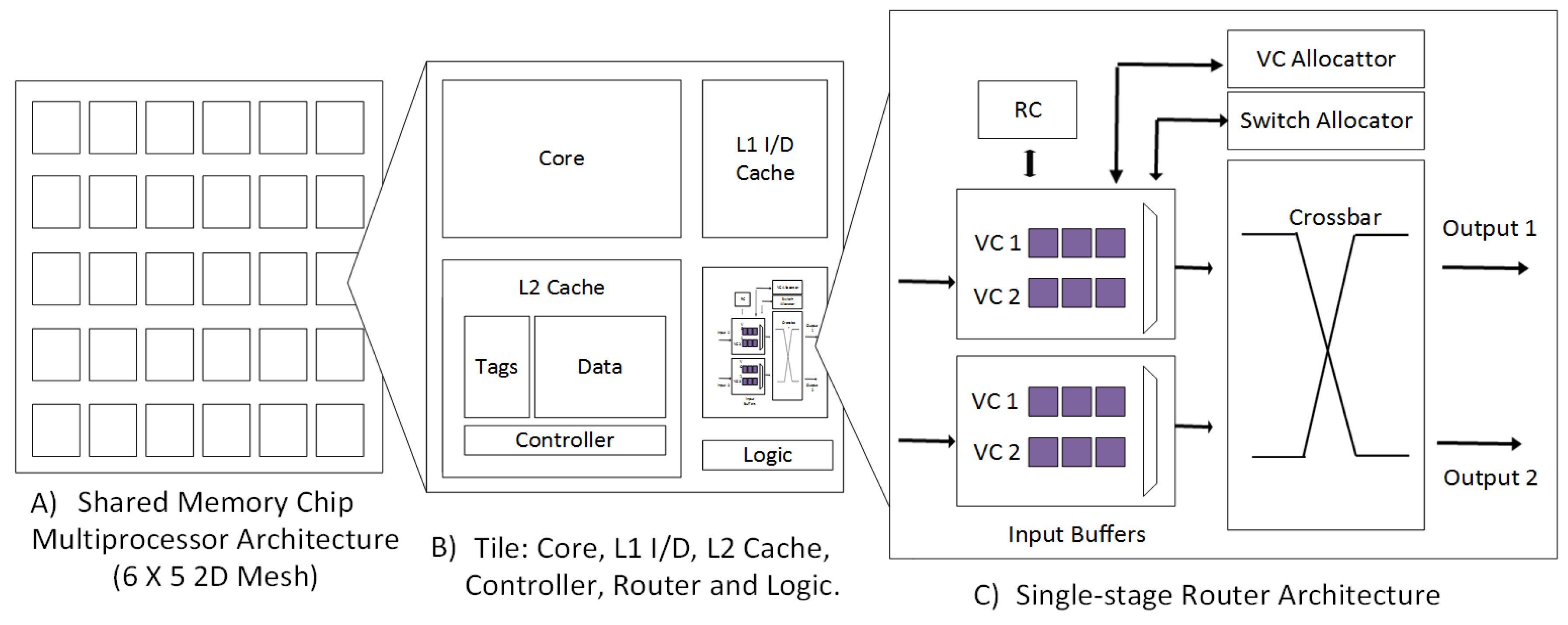
5.1. Router Architecture

The routers in NoC-based CMPs are the prime components responsible for interchanging data between nodes. Unfortunately, routers consume a significant amount of power. Particularly, when they are idle. As the network size increases, so does the amount of power dissipated by inactive routers. A traditional single-stage router architecture is comprised of an arbiter, buffer, crossbar, virtual channels, input and output ports as depicted in Figure 1c. Of all of these components, buffers and crossbars are the most important and the most consuming mechanisms; hence why efficient techniques are required to optimize them. Buffers in routers are installed at the input and output ports to temporally house packets, which cannot be forwarded immediately. Moreover, buffers are used for dynamic power management and equivalent to having cache and Translation Look-aside Buffer (TLB). Both are used for storing data. However, buffers in routers are used to store packets temporally while caches, on the other hand, are used to store frequent data shared between the processor and main memory; which can be re-used continuously. Similarly, TLBs are used to store data that can be accessed faster.
Subsequently, in buffers, virtual channels are embedded to divide a port into several virtual layers for simultaneous use. This process amplifies high throughout, high bandwidth and low latency at the cost of 33% of dynamic power loss in routers [68]. Particularly, the input buffers are considered to consume 45% of router power and occupy 15% of the area [69]. Therefore, balance is demanded in emerging buffered routers because aggressive implementation of buffer size inflates the power consumption, as well as the area overhead; on the other hand, diffident use of it will result in a poverty-stricken performance. Crossbars on the other hand are employed in routers to interconnect a set of input and output ports in a matrix form. Figure 1c depicts a typical n × n crossbar switch in a single-stage router architecture. Therefore, the size of the crossbar is relative to the number of processing elements employed in the CMPs. This exascale of the semiconductor during this deep-nanometre era has resulted in the multiplication of processing elements, thus expanding the size of the crossbar. The result of this is scalability issues, large area overhead and high power consumption [70]. As a matter of fact, Intel’s TeraFLOPS Processor [71] and MIT RAW [72] crossbars constitute a combined 40% of router power. For this reason, existing works have introduced novel techniques to improve power efficiency, the crossbar size, arbiter and buffer designs. For example, Palma et al. [73] presented a technique called T-bus-invert technology to effectively minimise the Hamming transition activity to improve the power consumption. In comparison to other schemes, the T-bus-invert saves more power regardless of the traffic patterns.
Over the years, several distinct design methodologies for routers have been proposed to not only enrich the performance of NoC-based CMPs, but to also ameliorate the power consumption. In this paper, we introduce several techniques that focus on power saving techniques at the buffer and crossbar level.

5.2. Alternative Buffer Solutions

Since buffers are major consumers of power in NoC, the bufferless router concept seeks to replace all buffers apart from the pipeline registers with flow control deflection algorithms to transmit packets instantly [74,75,76]. However, this concept has failed to overshadow the implementation of buffers for several reasons. Firstly, bufferless routers suffer extensively from performance degradation when the network reaches its saturation point. When the network reaches its saturation point, contention increases in the network resulting in penurious supplements of network requirements (low bandwidth, high latency and power consumption). Secondly, because bufferless routers are designed with one ejection port, multiple flits compete to eject at the same node when they arrive at the same time. In such cases, one flit concedes the output port to other, while the defeated flit is deflected off course, thus resulting in a livelock; livelock causes a surge in power consumption, bandwidth issues and high latency. For this purpose, the ejections ports in the routers proposed [74] have been optimized in a way that they can be increased from one to four. Unfortunately, in large networks, it is likely that more than four flits will arrive, and without the presence of buffers to house them temporally, a large number of flits will be deflected, of course, thus, increasing the power consumption. In addition to this, increasing the number of ejection ports increases the size of the crossbar, which in effect increases the NoC’s power. Similarly, to reduce deflection, Xiang et al. [77] proposed Deflection containment (Dec). In the proposed architecture, virtual routers been have developed in the physical router to form sub-networks. The introduction of an additional link allows all of the virtual routers to be joined together. This link allows packets that have been denied access in the current network to be transmitted to neighbouring sub-networks to contest for an ejection port.

5.2.1. Input Buffer Alternatives

Instead of the removing all of the buffers in the NoC, the following proposed techniques displace all of the buffers in the router and utilize them in other areas of the NoC to house packets. For example, Kodi et al. [78] proposed iDeal. In this architecture, dual function links are employed. The proposed architecture uses dynamic router buffer allocation instead of static buffer allocation to assign incoming flits to buffers that are not active. By using iDeal, the size of the buffer can be decreased while exiting repeaters are employed to function as buffers during network congestion. Similarly, DiTomaso et al. [68] proposed an architecture that improves power consumption using power-efficient Multi-Function Channel buffers (MFC) and enhances the performance through reversible links. The use of MFC enables the channel buffers to be utilized instead of the routers in the buffers. The work in [79] deals with power consumption by replacing the conventional SRAM with eDRAM. Significantly, buffer area was reduced by 52% and power by 43%.

5.2.2. Pipeline Stages

Since exiting design methodologies do not consider path availability and network congestion, the pipeline stages of routers keep increasing. Therefore, for an effective architecture, the following factors must be taken into consideration when proposing an optimized algorithm: path availability, buffer utilisation and network congestion. The following authors propose effective techniques for bypassing the buffering stage in one stage. Postman et al. [80] proposes a Low-Power Network-on-Chip Implementing the Token Flow Control Router Architecture With Swing-Reduced Interconnects (SWIFT) NoC, while Shenbagavelli [81] introduces virtual switching. The SWIFT NoC allows flits to pass through the buffering stage in a lesser number of cycles (one); ignoring the use of read/write power. Virtual channel switching on the other hand incorporates the benefits of circuit switching and packet switching to enable flits to bypass the buffering stage in one cycle.

5.2.3. Virtual Channel Low-Power Techniques

Excessive use of virtual channels guarantees the peak amount of throughput with an improved gain of low latency, while trading-off power for performance; a decision sometimes predefined by the designer or a dynamic algorithm depending on the workload. The latter is considered as a preferred option since the workload of application varies depending on the network congestion [82,83]. Inside the router architecture, input and output arbiters are employed to decide which input port gains access to their corresponding output port. The input arbiter decides which Virtual Channel (VC) should be granted access to use the crossbar. The header flit in the granted VC is then decoded by a header decoder to establish its requested output port. Since multiple ports can vie for the same output port, the output arbiter is employed to decide which input port can gain access to the output port. This optimized approach increases the arbitration complexity, as well as the power consumption. During the input port allocation, input VCs, header decoder and switch crossbars are the elements that are functioning while the output VCs remain idle. In reverse, during the output port allocation, all other elements are left idle while the output ports are utilized. The router dissipates much power during any of these two operations because of idle elements [84].
For this purpose, Muhammad et al. [84], Zhan et al. [85] and Nasirian et al. [86] all propose techniques that enable parts of the buffers, particular the virtual channels, to be switched-off to save power. The techniques proposed by Muhammad and Zhan allow the virtual channels to be divided into three groups, thus allowing a group to be activated/de-activated depending on the network workload. Nasirian et al., on the other hand, utilize a power-gating control unit to switch-off buffers from idle buffers after certain cycles of inactivity. Similarly, Phan et al. [87] deal with low power by employing a voltage-frequency controller to regulate the necessary voltage/frequency level required by the routers depending on the workload.

5.3. Low-Power Design Techniques for Crossbars

Low power consumption is the goal of many designers. Over the years, we have seen many ideas being put forward to lower the power of modern technology. This section of the paper introduces techniques that can applied to the crossbar to reduce power consumption.

5.3.1. Reduction of the Crossbar Size

The introduction of multi-core and many-core systems increases the crossbar size, thus increasing the power consumption [88,89]. To solve this problem, smaller crossbar sizes, such as the Clos and Benes, have emerged as an alternative solution [90,91,92,93].
Naik et al. [94] proposed an architecture comprised of hybrid circuit switched routers (buffered and bufferless router) with a three-stage Clos network. Experimental results show a huge reduction in power consumption and area. Similarly, Kim et al. introduced a two-crossbar router architecture in [95]. The proposed architecture has been constructed with smaller crossbars to reduce the size of the Virtual channel Allocator (VA), Switch Arbiter units (SA) and shorter logic depth. Likewise, Park et al. introduced an optimized crossbar [96], which has been downsized into two small crossbars. The integration of decomposition and segmentation in this architecture reduces the power consumption by 35%. Unfortunately, the drawback of using smaller size crossbars is that, in large-scale networks, there will be an increase in average latency, thus resulting in performance degradation. Therefore, such techniques trade-off performance for power efficiency.

5.3.2. Low-Power Switching Algorithm Techniques

FallahRad et al. [97] proposed Cirket. CirKet is an effective technique that incorporates the advantages of both packet switched and circuit switched routers. In the proposed architecture, messages are divided into two separate groups: high priority and low priority. With Cirket, the messages of high priority are transmitted using circuit switching while the lower priority messages are transmitted using packet switching. In addition to this, the use of CirKet allows power rails to be disconnected while power gating is utilized to disable idle parts of the router during transmission.

6. Conclusions

Various contributions have been made to tackle the problem caused by inefficient consumption of power in cache and router architectures. However, due to the ever-growing transistor density with technology, novel power-saving techniques are required for these components. In this paper, a survey of recent architectural techniques for improving cache and router power consumption is presented; particularly, the power-saving techniques for dynamic and leakage power consumption of the caches. NoC router techniques at the buffer and crossbar level have also been presented with a view toward looking at other ways of saving power; whether it being the removal of buffers, displacement of buffers and utilizing them in the links or using two small crossbars instead of a large crossbar. Consequently, the combination of some of the architectures presented, if employed, can help improve the amount of power consumed by NoC-based CMPs’ resources, which can either be removed or switched off. This work serves as a quick reference guide for the power-saving techniques, recent commercial chips, caches and NoC router architectures.

Author Contributions

All authors contributed equally to this work.

Conflicts of Interest

The authors declare no conflict of interest.

References

  1. Valero, A.; Sahuquillo, J.; Petit, S.; López, P.; Duato, J. Design of Hybrid Second-Level Caches. IEEE Trans. Comput. 2015, 64, 1884–1897. [Google Scholar] [CrossRef]
  2. Neishaburi, M.H.; Zilic, Z. A Fault Tolerant Hierarchical Network on Chip Router Architecture. In Proceedings of the IEEE International Symposium on Defect and Fault Tolerance in VLSI and Nanotechnology Systems, Vancouver, BC, Canada, 3–5 October 2011; pp. 445–453. [Google Scholar]
  3. Jebaseeli, A.D.; Kiruba, M. Design of low power L2 cache architecture using partial way tag information. In Proceedings of the International Conference on Green Computing Communication and Electrical Engineering (ICGCCEE), Coimbatore, India, 6–8 March 2014; pp. 1–6. [Google Scholar]
  4. Chen, L.; Pinkston, T.M. NoRD: Node-Router Decoupling for Effective Power-gating of On-Chip Routers. In Proceedings of the 45th Annual IEEE/ACM International Symposium on Microarchitecture, Vancouver, BC, Canada, 1–5 December 2012; pp. 270–281. [Google Scholar]
  5. Sun, C.; Chen, C.H.O.; Kurian, G.; Wei, L.; Miller, J.; Agarwal, A.; Peh, L.S.; Stojanovic, V. DSENT—5A Tool Connecting Emerging Photonics with Electronics for Opto-Electronic Networks-on-Chip Modeling. In Proceedings of the 2012 Sixth IEEE/ACM International Symposium on Networks on Chip (NoCS), Lyngby, Denmark, 9–11 May 2012; pp. 201–210. [Google Scholar]
  6. Kudithipudi, D.; Petko, S.; John, E.B. Caches for Multimedia Workloads: Power and Energy Tradeoffs. IEEE Trans. Multimed. 2008, 10, 1013–1021. [Google Scholar] [CrossRef]
  7. Lin, I.C.; Chiou, J.N. High-Endurance Hybrid Cache Design in CMP Architecture With Cache Partitioning and Access-Aware Policies. IEEE Trans. Very Large Scale Integr. Syst. 2015, 23, 2149–2161. [Google Scholar] [CrossRef]
  8. Monchiero, M.; Canal, R.; Gonzalez, A. Using Coherence Information and Decay Techniques to Optimize L2 Cache Leakage in CMPs. In Proceedings of the International Conference on Parallel Processing, Vienna, Austria, 22–25 September 2009; pp. 1–8. [Google Scholar]
  9. Fischer, K.; Chang, H.K.; Ingerly, D.; Jin, I.; Kilambi, H.; Longun, J.; Patel, R.; Pelto, C.; Petersburg, C.; Plekhanov, P.; et al. Performance enhancement for 14nm high volume manufacturing microprocessor and system on a chip processes. In Proceedings of the IEEE International Interconnect Technology Conference/Advanced Metallization Conference (IITC/AMC), San Jose, CA, USA, 23–26 May 2016; pp. 5–7. [Google Scholar]
  10. Mittal, S.; Vetter, J.S. A Survey Of Techniques for Architecting DRAM Caches. IEEE Trans. Parallel Distrib. Syst. 2016, 27, 1852–1863. [Google Scholar] [CrossRef]
  11. An Overview of Cache; Intel: Santa Clara, CA, USA, 2015; pp. 1–4. Available online: http://download.intel.com/design/intarch/papers/cache6.pdf (accessed on 1 January 2017).
  12. Mittal, S.; Cao, Y.; Zhang, Z. MASTER: A Multicore Cache Energy-Saving Technique Using Dynamic Cache Reconfiguration. IEEE Trans. Very Large Scale Integr. Syst. 2014, 22, 1653–1665. [Google Scholar] [CrossRef]
  13. Mittal, S. A Survey of Architectural Techniques for Improving Cache Power Efficiency. Sustain. Comput. Inf. Syst. 2013, 4, 43–48. [Google Scholar] [CrossRef]
  14. Warnock, J.; Chan, Y.; Harrer, H.; Carey, S.; Salem, G.; Malone, D.; Puri, R.; Zitz, J.A.; Jatkowski, A.; Strevig, G.; et al. Circuit and Physical Design of the zEnterprise™ EC12 Microprocessor Chips and Multi-Chip Module. IEEE J. Solid State Circuits 2014, 49, 9–18. [Google Scholar]
  15. Shum, C.K.; Busaba, F.; Jacobi, C. IBM zEC12: The Third-Generation High-Frequency Mainframe Microprocessor. IEEE Micro 2013, 33, 38–47. [Google Scholar] [CrossRef]
  16. Haupt, M.; Brunschwiller, T.; Keller, J.; Ozsun, O. Heat transfer modelling of a dual-side cooled microprocessor chip stack with embedded micro-channels. In Proceedings of the 21st International Workshop on Thermal Investigations of ICs and Systems (THERMINIC), Paris, France, 30 September–2 October 2015; pp. 1–4. [Google Scholar]
  17. Warnock, J.; Chan, Y.H.; Harrer, H.; Rude, D.; Puri, R.; Carey, S.; Salem, G.; Mayer, G.; Chan, Y.H.; Mayo, M.; et al. 5.5 GHz system z microprocessor and multi-chip module. In Proceedings of the IEEE International Solid-State Circuits Conference Digest of Technical Papers, San Francisco, CA, USA, 17–21 February 2013; pp. 46–47. [Google Scholar]
  18. Choi, M.; Jang, T.; Bang, S.; Shi, Y.; Blaauw, D.; Sylvester, D. A 110 nW Resistive Frequency Locked On-Chip Oscillator with 34.3 ppm/°C Temperature Stability for System-on-Chip Designs. IEEE J. Solid State Circuits 2016, 51, 2106–2118. [Google Scholar] [CrossRef]
  19. Yen, C.H.; Chen, C.H.; Chen, K.C. A memory-efficient NoC system for OpenCL many-core platform. In Proceedings of the IEEE International Symposium on Circuits and Systems (ISCAS), Lisbon, Portugal, 24–27 May 2015; pp. 1386–1389. [Google Scholar]
  20. Arima, E.; Noguchi, H.; Nakada, T.; Miwa, S.; Takeda, S.; Fujita, S.; Nakamura, H. Immediate sleep: Reducing energy impact of peripheral circuits in STT-MRAM caches. In Proceedings of the 33rd IEEE International Conference on Computer Design (ICCD), New York, NY, USA, 18–21 October 2015; pp. 149–156. [Google Scholar]
  21. Khaitan, S.K.; McCalley, J.D. A hardware-based approach for saving cache energy in multicore simulation of power systems. In Proceedings of the IEEE Power Energy Society General Meeting, Vancouver, BC, Canada, 21–25 July 2013; pp. 1–5. [Google Scholar]
  22. Wang, Y.; Roy, S.; Ranganathan, N. Run-time power-gating in caches of GPUs for leakage energy savings. In Proceedings of the Design, Automation Test in Europe Conference Exhibition (DATE), Dresden, Germany, 12–16 March 2012; pp. 300–303. [Google Scholar]
  23. Bengueddach, A.; Senouci, B.; Niar, S.; Beldjilali, B. Energy consumption in reconfigurable mpsoc architecture: Two-level caches optimization oriented approach. In Proceedings of the 8th IEEE Design and Test Symposium, Marrakesh, Morocco, 16–18 December 2013; pp. 1–6. [Google Scholar]
  24. Mittal, S.; Zhang, Z.; Vetter, J.S. FlexiWay: A cache energy saving technique using fine-grained cache reconfiguration. In Proceedings of the IEEE 31st International Conference on Computer Design (ICCD), Asheville, NC, USA, 6–9 October 2013; pp. 100–107. [Google Scholar]
  25. Mittal, S.; Zhang, Z.; Cao, Y. CASHIER: A Cache Energy Saving Technique for QoS Systems. In Proceedings of the 26th International Conference on VLSI Design and 2013 12th International Conference on Embedded Systems, Pune, India, 5–10 January 2013; pp. 43–48. [Google Scholar]
  26. Wang, W.; Mishra, P. System-Wide Leakage-Aware Energy Minimization Using Dynamic Voltage Scaling and Cache Reconfiguration in Multitasking Systems. IEEE Trans. Very Large Scale Integr. Syst. 2012, 20, 902–910. [Google Scholar] [CrossRef]
  27. Kadjo, D.; Kim, H.; Gratz, P.; Hu, J.; Ayoub, R. Power gating with block migration in chip-multiprocessor last-level caches. In Proceedings of the IEEE 31st International Conference on Computer Design (ICCD), Asheville, NC, USA, 6–9 October 2013; pp. 93–99. [Google Scholar]
  28. Cheng, W.K.; Cheng, P.C.; Li, X.L. Adaptive page allocation of DRAM/PCRAM hybrid memory architecture. In Proceedings of the 5th International Symposium on Next-Generation Electronics (ISNE), Hsinchu, Taiwan, 4–6 May 2016; pp. 1–2. [Google Scholar]
  29. De Abreu Silva, B.; Cuminato, L.A.; Bonato, V. Reducing the overall cache miss rate using different cache sizes for Heterogeneous Multi-core Processors. In Proceedings of the 2012 International Conference on Reconfigurable Computing and FPGAs, Cancun, Mexico, 5–7 December 2012; pp. 1–6. [Google Scholar]
  30. Bardine, A.; Comparetti, M.; Foglia, P.; Prete, C.A. Evaluation of Leakage Reduction Alternatives for Deep Submicron Dynamic Nonuniform Cache Architecture Caches. IEEE Trans. Very Large Scale Integr. Syst. 2014, 22, 185–190. [Google Scholar] [CrossRef]
  31. Zhu, H.; Kursun, V. Triple-threshold-voltage 9-transistor SRAM cell for data stability and energy-efficiency at ultra-low power supply voltages. In Proceedings of the 26th International Conference on Microelectronics (ICM), Seoul, Korea, 13–21 August 2014; pp. 176–179. [Google Scholar]
  32. Chen, K.C.J.; Chao, C.H.; Wu, A.Y.A. Thermal-Aware 3D Network-On-Chip (3D NoC) Designs: Routing Algorithms and Thermal Managements. IEEE Circuits Syst. Mag. 2015, 15, 45–69. [Google Scholar] [CrossRef]
  33. Hameed, F.; Tahoori, M.B. Architecting STT Last-Level-Cache for performance and energy improvement. In Proceedings of the 17th International Symposium on Quality Electronic Design (ISQED), Santa Clara, CA, USA, 15–16 March 2016; pp. 319–324. [Google Scholar]
  34. Rossi, D.; Tenentes, V.; Khursheed, S.; Al-Hashimi, B.M. BTI and leakage aware dynamic voltage scaling for reliable low power cache memories. In Proceedings of the IEEE 21st International On-Line Testing Symposium (IOLTS), Halkidiki, Greece, 6–8 July 2015; pp. 194–199. [Google Scholar]
  35. Jing, N.; Jiang, L.; Zhang, T.; Li, C.; Fan, F.; Liang, X. Energy-Efficient eDRAM-Based On-Chip Storage Architecture for GPGPUs. IEEE Trans. Comput. 2016, 65, 122–135. [Google Scholar] [CrossRef]
  36. Chakraborty, S.; Das, S.; Kapoor, H.K. Performance Constrained Static Energy Reduction Using Way-Sharing Target-Banks. In Proceedings of the IEEE International Parallel and Distributed Processing Symposium Workshop, Hyderabad, India, 25–29 May 2015; pp. 444–453. [Google Scholar]
  37. Sampaio, F.; Shafique, M.; Zatt, B.; Bampi, S.; Henkel, J. Approximation-aware Multi-Level Cells STT-RAM cache architecture. In Proceedings of the International Conference on Compilers, Architecture and Synthesis for Embedded Systems (CASES), Amsterdam, The Netherlands, 4–9 October 2015; pp. 79–88. [Google Scholar]
  38. Chien, T.K.; Chiou, L.Y.; Lee, C.C.; Chuang, Y.C.; Ke, S.H.; Sheu, S.S.; Li, H.Y.; Wang, P.H.; Ku, T.K.; Tsai, M.J.; et al. An energy-efficient nonvolatile microprocessor considering software-hardware interaction for energy harvesting applications. In Proceedings of the International Symposium on VLSI Design, Automation and Test (VLSI-DAT), Hsinchu, Taiwan, 25–27 April 2016; pp. 1–4. [Google Scholar]
  39. Saez, J.C.; Prieto, M.; Fedorova, A.; Blagodurov, S. A Comprehensive Scheduler for Asymmetric Multicore Systems. In Proceedings of the 5th European Conference on Computer Systems, Paris, France, 13–16 April 2010; pp. 139–152. [Google Scholar]
  40. Manoj, P.D.S.; Yu, H. Cyber-physical management for heterogeneously integrated 3D thousand-core on-chip microprocessor. In Proceedings of the IEEE International Symposium on Circuits and Systems (ISCAS2013), Beijing, China, 19–23 May 2013; pp. 533–536. [Google Scholar]
  41. Lou, M.; Wu, L.; Shi, S.; Lu, P. An energy-efficient two-level cache architecture for chip multiprocessors. In Proceedings of the Fifth International Conference on Computing, Communications and Networking Technologies (ICCCNT), Hefei, China, 11–13 July 2014; pp. 1–5. [Google Scholar]
  42. Aneesh Kumar, A.G.; Janeera, D.A.; Ramesh, M. Power and performance efficient secondary cache using tag bloom architecture. In Proceedings of the International Conference on Electronics and Communication Systems (ICECS), Coimbatore, India, 13–14 Febuary 2014; pp. 1–5. [Google Scholar]
  43. Subha, S. A reconfigurable cache architecture. In Proceedings of the International Conference on High Performance Computing and Applications (ICHPCA), Bhubaneswar, India, 22–24 December 2014; pp. 1–5. [Google Scholar]
  44. Ahn, J.; Yoo, S.; Choi, K. Prediction Hybrid Cache: An Energy-Efficient STT-RAM Cache Architecture. IEEE Trans. Comput. 2016, 65, 940–951. [Google Scholar] [CrossRef]
  45. Lee, J.; Kim, S. Filter Data Cache: An Energy-Efficient Small L0 Data Cache Architecture Driven byMiss Cost Reduction. IEEE Trans. Comput. 2015, 64, 1927–1939. [Google Scholar] [CrossRef]
  46. Mallya, N.B.; Patil, G.; Raveendran, B. Way Halted Prediction Cache: An Energy Efficient Cache Architecture for Embedded Processors. In Proceedings of the 2015 28th International Conference on VLSI Design, Bangalore, India, 3–7 January 2015; pp. 65–70. [Google Scholar]
  47. Cilku, B.; Prokesch, D.; Puschner, P. A Time-Predictable Instruction-Cache Architecture that Uses Prefetching and Cache Locking. In Proceedings of the IEEE International Symposium on Object/Component/Service-Oriented Real-Time Distributed Computing Workshops, Auckland, New Zealand, 13–17 April 2015; pp. 74–79. [Google Scholar]
  48. Kalla, P.; Hu, X.S.; Henkel, J. Distance-based recent use (DRU): An enhancement to instruction cache replacement policies for transition energy reduction. IEEE Trans. Very Large Scale Integr. Syst. 2006, 14, 69–80. [Google Scholar] [CrossRef]
  49. Mohammadi, M.; Han, S.; Aamodt, T.M.; Dally, W.J. On-Demand Dynamic Branch Prediction. IEEE Comput. Arch. Lett. 2015, 14, 50–53. [Google Scholar] [CrossRef]
  50. Nadgir, A.; Kandemir, M.; Chen, G.; Chen, G. An access pattern based energy management strategy for instruction caches. In Proceedings of the IEEE International [Systems-on-Chip] SOC Conference, Portland, OR, USA, 17–20 September 2003; pp. 175–178. [Google Scholar]
  51. Ray, A.; Choudhry, A. Time optimization of instruction execution in FPGA using embedded systems. In Proceedings of the International Conference on Futuristic Trends on Computational Analysis and Knowledge Management (ABLAZE), New Delhi, India, 25–27 February 2015; pp. 566–572. [Google Scholar]
  52. Li, T.; John, L.K. OS-aware tuning: Improving instruction cache energy efficiency on system workloads. In Proceedings of the IEEE International Performance Computing and Communications Conference, Phoenix, AZ, USA, 10–12 April 2006. [Google Scholar]
  53. Zhang, C.; Zhang, X.; Yan, Y. Multi-column implementations for cache associativity. In Proceedings of the International Conference on Computer Design VLSI in Computers and Processors, Austin, TX, USA, 12–15 October 1997; pp. 504–509. [Google Scholar]
  54. Kim, H.; Gratz, P. Leveraging Unused Cache Block Words to Reduce Power in CMP Interconnect. IEEE Comput. Arch. Lett. 2010, 9, 33–36. [Google Scholar]
  55. Datta, A.K.; Patel, R. CPU Scheduling for Power/Energy Management on Multicore Processors Using Cache Miss and Context Switch Data. IEEE Trans. Parallel Distrib. Syst. 2014, 25, 1190–1199. [Google Scholar] [CrossRef]
  56. Kim, N.; Ahn, J.; Seo, W.; Choi, K. Energy-efficient exclusive last-level hybrid caches consisting of SRAM and STT-RAM. In Proceedings of the IFIP/IEEE International Conference on Very Large Scale Integration (VLSI-SoC), Daejeon, Korea, 5–7 October 2015; pp. 183–188. [Google Scholar]
  57. Grani, P.; Proietti, R.; Cheung, S.; Yoo, S.J.B. Flat-Topology High-Throughput Compute Node with AWGR-Based Optical-Interconnects. J. Lightwave Technol. 2016, 34, 2959–2968. [Google Scholar] [CrossRef]
  58. Farmahini-Farahani, A.; Ahn, J.H.; Morrow, K.; Kim, N.S. DRAMA: An Architecture for Accelerated Processing Near Memory. IEEE Comput. Arch. Lett. 2015, 14, 26–29. [Google Scholar] [CrossRef]
  59. Goudarzi, M.; Ishihara, T.; Yasuura, H. A Software Technique to Improve Yield of Processor Chips in Presence of Ultra-Leaky SRAM Cells Caused by Process Variation. In Proceedings of the Asia and South Pacific Design Automation Conference, Yokohama, Japan, 23–26 January 2007; pp. 878–883. [Google Scholar]
  60. Samavatian, M.H.; Abbasitabar, H.; Arjomand, M.; Sarbazi-Azad, H. An efficient STT-RAM last level cache architecture for GPUs. In Proceedings of the 51st ACM/EDAC/IEEE Design Automation Conference (DAC), San Francisco, CA, USA, 1–5 June 2014; pp. 1–6. [Google Scholar]
  61. Lee, D.; Choi, K. Energy-efficient partitioning of hybrid caches in multi-core architecture. In Proceedings of the 22nd International Conference on Very Large Scale Integration (VLSI-SoC), Playa del Carmen, Mexico, 6–8 October 2014; pp. 1–6. [Google Scholar]
  62. Dai, J.; Wang, L. An Energy-Efficient L2 Cache Architecture Using Way Tag Information Under Write-Through Policy. IEEE Trans. Very Large Scale Integr. Syst. 2013, 21, 102–112. [Google Scholar] [CrossRef]
  63. Lee, J.; Woo, D.H.; Kim, H.; Azimi, M. GREEN Cache: Exploiting the Disciplined Memory Model of OpenCL on GPUs. IEEE Trans. Comput. 2015, 64, 3167–3180. [Google Scholar] [CrossRef]
  64. Tu, C.Y.; Chang, Y.Y.; King, C.T.; Chen, C.T.; Wang, T.Y. Traffic-aware frequency scaling for balanced on-chip networks on GPGPUs. In Proceedings of the 20th IEEE International Conference on Parallel and Distributed Systems (ICPADS), Hsinchu, Taiwan, 16–19 December 2014; pp. 87–94. [Google Scholar]
  65. Agyeman, M.O.; Ahmadinia, A.; Shahrabi, A. Low power heterogeneous 3D Networks-on-Chip architectures. In Proceedings of the 2011 International Conference on High Performance Computing Simulation, Istanbul, Turkey, 4–8 July 2011. [Google Scholar]
  66. Hoskote, Y.; Vangal, S.; Singh, A.; Borkar, N.; Borkar, S. A 5-GHz Mesh Interconnect for a Teraflops Processor. IEEE Micro 2007, 27, 51–61. [Google Scholar] [CrossRef]
  67. Taylor, M.B.; Psota, J.; Saraf, A.; Shnidman, N.; Strumpen, V.; Frank, M.; Amarasinghe, S.; Agarwal, A.; Lee, W.; Miller, J.; et al. Evaluation of the Raw microprocessor: An exposed-wire-delay architecture for ILP and streams. In Proceedings of the 31st Annual International Symposium on Computer Architecture, München, Germany, 19–23 June 2004; pp. 2–13. [Google Scholar]
  68. DiTomaso, D.; Kodi, A.K.; Louri, A.; Bunescu, R. Resilient and Power-Efficient Multi-Function Channel Buffers in Network-on-Chip Architectures. IEEE Trans. Comput. 2015, 64, 3555–3568. [Google Scholar] [CrossRef]
  69. Kundu, P. On-Die Interconnects for Next Generation CMPs. In Proceedings of the Workshop on On- and Off-Chip Interconnection Networks for Multicore Systems, Stanford, CA, USA, 6–7 December 2006. [Google Scholar]
  70. Sewell, K.; Dreslinski, R.G.; Manville, T.; Satpathy, S.; Pinckney, N.; Blake, G.; Cieslak, M.; Das, R.; Wenisch, T.F.; Sylvester, D.; et al. Swizzle-Switch Networks for Many-Core Systems. IEEE J. Emerg. Sel. Top. Circuits Syst. 2012, 2, 278–294. [Google Scholar] [CrossRef]
  71. Vangal, S.R.; Howard, J.; Ruhl, G.; Dighe, S.; Wilson, H.; Tschanz, J.; Finan, D.; Singh, A.; Jacob, T.; Jain, S.; et al. An 80-Tile Sub-100-W TeraFLOPS Processor in 65-nm CMOS. IEEE J. Solid State Circuits 2008, 43, 29–41. [Google Scholar] [CrossRef]
  72. Taylor, M.B.; Kim, J.; Miller, J.; Wentzlaff, D.; Ghodrat, F.; Greenwald, B.; Hoffman, H.; Johnson, P.; Lee, J.W.; Lee, W.; et al. The Raw microprocessor: A computational fabric for software circuits and general-purpose programs. IEEE Micro 2002, 22, 25–35. [Google Scholar] [CrossRef]
  73. Palma, J.C.S.; Indrusiak, L.S.; Moraes, F.G.; Reis, R.; Glesner, M. Reducing the Power Consumption in Networks-on-Chip through Data Coding Schemes. In Proceedings of the 2007 14th IEEE International Conference on Electronics, Circuits and Systems, Marrakech, Morocco, 11–14 December 2007; pp. 1007–1010. [Google Scholar]
  74. Feng, C.; Liao, Z.; Lu, Z.; Jantsch, A.; Zhao, Z. Performance analysis of on-chip bufferless router with multi-ejection ports. In Proceedings of the IEEE 11th International Conference on ASIC (ASICON), Chengdu, China, 3–6 November 2015; pp. 1–4. [Google Scholar]
  75. Fallin, C.; Craik, C.; Mutlu, O. CHIPPER: A low-complexity bufferless deflection router. In Proceedings of the IEEE 17th International Symposium on High Performance Computer Architecture, San Antonio, TX, USA, 12–16 February 2011; pp. 144–155. [Google Scholar]
  76. Daya, B.K.; Peh, L.S.; Chandrakasan, A.P. Towards High-Performance Bufferless NoCs with SCEPTER. IEEE Comput. Arch. Lett. 2016, 15, 62–65. [Google Scholar] [CrossRef]
  77. Xiang, X.Y.; Tzeng, N.F. Deflection Containment for Bufferless Network-on-Chips. In Proceedings of the IEEE International Parallel and Distributed Processing Symposium (IPDPS), Chicago, IL, USA, 23–27 May 2016; pp. 113–122. [Google Scholar]
  78. Kodi, A.K.; Sarathy, A.; Louri, A.; Wang, J. Adaptive inter-router links for low-power, area-efficient and reliable Network-on-Chip (NoC) architectures. In Proceedings of the Asia and South Pacific Design Automation Conference, Yokohama, Japan, 19–22 January 2009; pp. 1–6. [Google Scholar]
  79. Li, C.; Ampadu, P. A compact low-power eDRAM-based NoC buffer. In Proceedings of the IEEE/ACM International Symposium on Low Power Electronics and Design (ISLPED), Rome, Italy, 22–24 July 2015; pp. 116–121. [Google Scholar]
  80. Postman, J.; Krishna, T.; Edmonds, C.; Peh, L.S.; Chiang, P. SWIFT: A Low-Power Network-On-Chip Implementing the Token Flow Control Router Architecture With Swing-Reduced Interconnects. IEEE Trans. Very Large Scale Integr. Syst. 2013, 1432–1446. [Google Scholar] [CrossRef]
  81. Shenbagavalli, S.; Karthikeyan, S. An efficient low power NoC router architecture design. In Proceedings of the Online International Conference on Green Engineering and Technologies (IC-GET), Coimbatore, India, 27 November 2015; pp. 1–8. [Google Scholar]
  82. Sharma, P.K.; Bairathi, R. Study and analysis of the behavior of a generic mesh architecture of NoC routers. In Proceedings of the International MultiConference of Engineers and Computer Scientists, Hong Kong, China, 17–19 March 2010; pp. 17–19. [Google Scholar]
  83. Nadi, M.; Ghadiry, M.H.; Dermany, M.K. The Effect of Number of Virtual Channels on NoC EDP. J. Appl. Math. Informat. 2010, 3, 539–551. [Google Scholar]
  84. Muhammad, S.T.; El-Moursy, M.A.; El-Moursy, A.A.; Refaat, A.M. Optimization for traffic-based virtual channel activation low-power NoC. In Proceedings of the International Conference on Energy Aware Computing Systems Applications (ICEAC), Toledo, Spain, 22–28 July 2015; pp. 1–4. [Google Scholar]
  85. Zhan, J.; Ouyang, J.; Ge, F.; Zhao, J.; Xie, Y. Hybrid Drowsy SRAM and STT-RAM Buffer Designs for Dark-Silicon-Aware NoC. IEEE Trans. Very Large Scale Integr. Syst. 2016, 24, 3041–3054. [Google Scholar] [CrossRef]
  86. Nasirian, N.; Bayoumi, M. Low-latency power-efficient adaptive router design for network-on-chip. In Proceedings of the 28th IEEE International System-on-Chip Conference (SOCC), Kohala Coast, HI, USA, 27–29 August 2015; pp. 287–291. [Google Scholar]
  87. Phan, H.P.; Tran, X.T. Fuzzy-logic based low power solution for Network-on-Chip architectures. In Proceedings of the 2016 International Conference on Advanced Technologies for Communications (ATC), Hanoi City, Vietnam, 12–14 October 2016; pp. 334–338. [Google Scholar]
  88. Agyeman, M.O.; Ahmadinia, A.; Shahrabi, A. Efficient routing techniques in heterogeneous 3D Networks-on-Chip. Parallel Comput. 2013, 39, 389–407. [Google Scholar] [CrossRef]
  89. Agyeman, M.O.; Ahmadinia, A.; Shahrabi, A. Heterogeneous 3D Network-on-Chip Architectures: Area and Power Aware Design Techniques. J. Circuits Syst. Comput. 2013, 22, 1350016. [Google Scholar] [CrossRef]
  90. Xia, Y.; Hamdi, M.; Chao, H.J. A Practical Large-Capacity Three-Stage Buffered Clos-Network Switch Architecture. IEEE Trans. Parallel Distrib. Syst. 2016, 27, 317–328. [Google Scholar] [CrossRef]
  91. Yang, S.; Xin, S.; Zhao, Z.; Wu, B. Minimizing Packet Delay via Load Balancing in Clos Switching Networks for Datacenters. In Proceedings of the International Conference on Networking and Network Applications (NaNA), Hokkaido, Japan, 23–25 July 2016; pp. 23–28. [Google Scholar]
  92. Zhang, J.; Gu, H. A partially adaptive routing algorithm for Benes network on chip. In Proceedings of the 2nd IEEE International Conference on Computer Science and Information Technology, Beijing, China, 8–11 August 2009; pp. 614–618. [Google Scholar]
  93. Jiang, Y.; Yang, M. On circuit design of on-chip non-blocking interconnection networks. In Proceedings of the 27th IEEE International System-on-Chip Conference (SOCC), Seattle, WA, USA, 3–5 November 2014; pp. 192–197. [Google Scholar]
  94. Naik, A.; Ramesh, T.K. Efficient Network on Chip (NoC) using heterogeneous circuit switched routers. In Proceedings of the International Conference on VLSI Systems, Architectures, Technology and Applications (VLSI-SATA), Tamil Nadu, India, 10–12 January 2016; pp. 1–6. [Google Scholar]
  95. Kim, J.; Nicopoulos, C.; Park, D. A Gracefully Degrading and Energy-Efficient Modular Router Architecture for On-Chip Networks. In Proceedings of the 33rd International Symposium on Computer Architecture (ISCA’06), Boston, MA, USA, 17–21 June 2006; pp. 4–15. [Google Scholar]
  96. Park, D.; Vaidya, A.; Kumar, A.; Azimi, M. MoDe-X: Microarchitecture of a Layout-Aware Modular Decoupled Crossbar for On-Chip Interconnects. IEEE Trans. Comput. 2014, 63, 622–636. [Google Scholar]
  97. FallahRad, M.; Patooghy, A.; Ziaeeziabari, H.; Taheri, E. CirKet: A Performance Efficient Hybrid Switching Mechanism for NoC Architectures. In Proceedings of the Euromicro Conference on Digital System Design (DSD), Limassol, Cyprus, 31 August–2 September 2016; pp. 123–130. [Google Scholar]
Figure 1. 2D Network-on-Chip-based Chip-Multiprocessor (NoC-based CMP).
Jlpea 07 00014 g001
Figure 2. Power consumption.
Jlpea 07 00014 g002
Figure 3. Cache architecture.
Jlpea 07 00014 g003
Figure 4. First Level Cache (FLC).
Jlpea 07 00014 g004
Figure 5. Low Level Cache (LLC).
Jlpea 07 00014 g005
Figure 6. Drowsy cache.
Jlpea 07 00014 g006
Figure 7. Power gating.
Jlpea 07 00014 g007
Figure 8. First Level Cache (FLC).
Jlpea 07 00014 g008
Figure 9. New caching.
Jlpea 07 00014 g009

