
Design of a Wideband Antenna for Wireless Network-On-Chip in Multimedia Applications


Abstract
:1. Introduction
- -
- poor scalability;
- -
- increased delay when transferring high data rates—at several Gb/s—among cores and/or memories placed at distances greater than 1 cm;
- -
- increased power consumption to switch—at continuously increasing frequencies—the large capacitance offered by long metal wires.
2. Design of the On-Chip High-Bandwidth Antenna
- -
- custom circuitry for antenna–driver matching
- -
- rounded corners to reduce charge accumulation phenomena
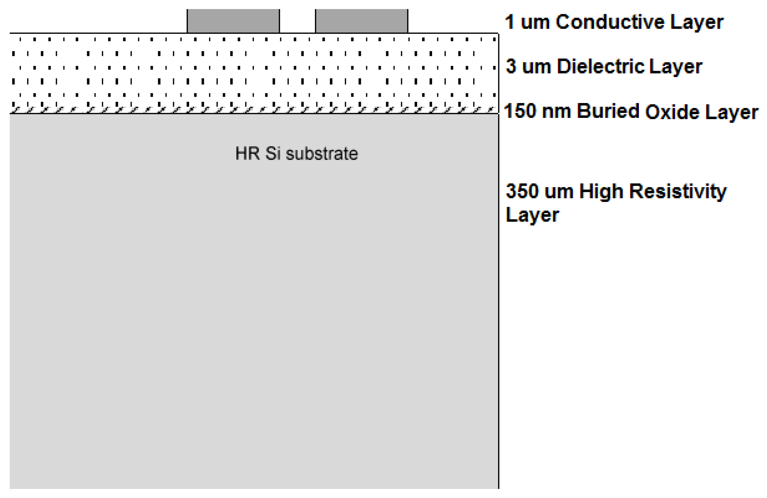
- (1)
- a dielectric layer with a thickness of about 3 µm and a relative dielectric permittivity ɛr of about 3.5;
- (2)
- a buried oxide layer with a thickness of 150 nm (a value typical for SOI manufacturing technology, see p. 11 of [72]) and a relative dielectric permittivity ɛr of about 4;
- (3)
- a high-resistivity (HR) layer with a thickness of 350 µm (a value typical for wafers used in RF applications, see [73]) and the following electrical parameters: ρ = 5 kΩ·cm and ɛr = 11.7.
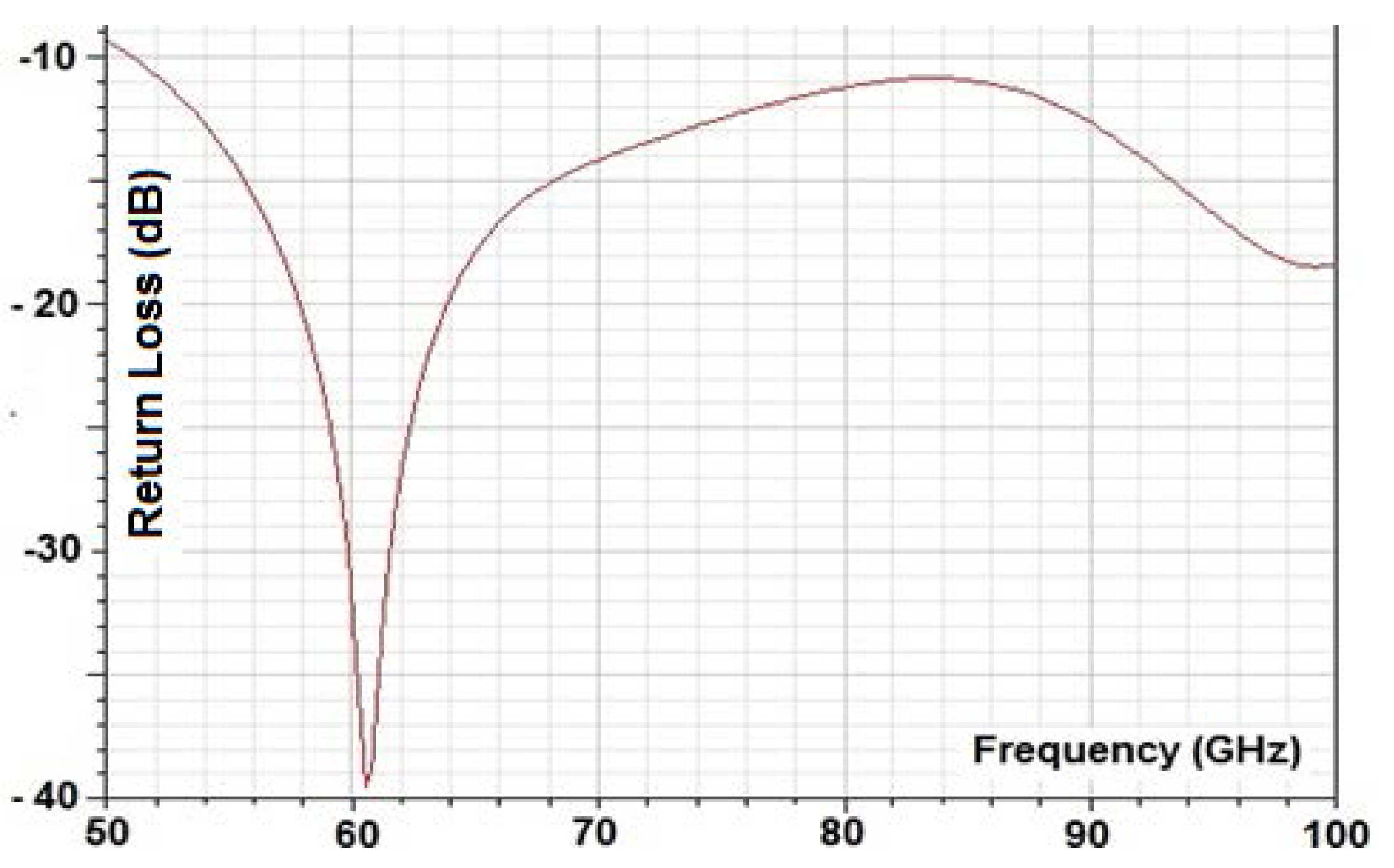
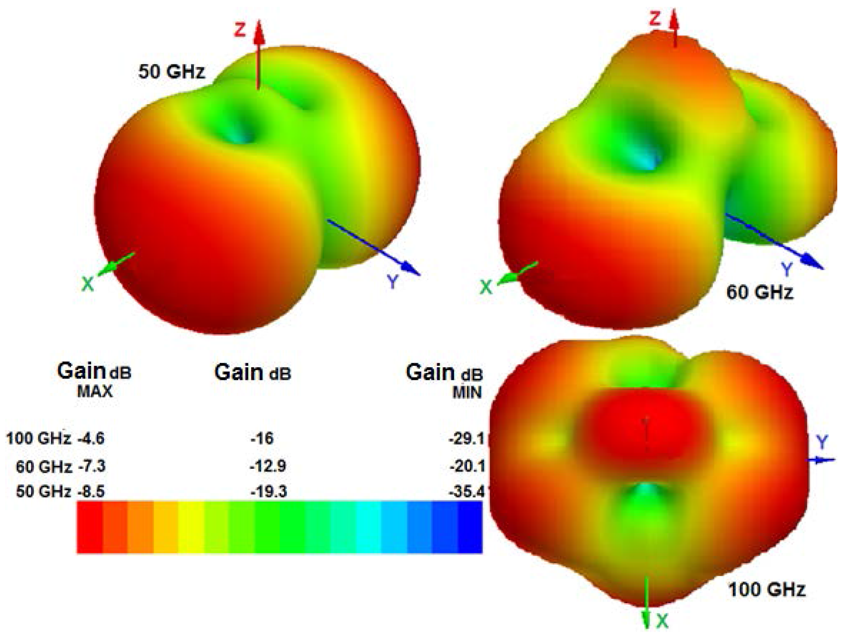
3. Antenna Characterization
4. Comparison of the Designed Antenna vs. the State-of-the-Art
5. Impact of the Proposed Antenna on the NoC Infrastructure Performance
6. Conclusions
Conflicts of Interest
References
- Torres, L.; Benoit, P.; Sassatelli, G.; Robert, M.; Clermidy, F.; Puschini, D. An Introduction to Multi-Core System-on-Chip: Trends and Challenges. In Multiprocessor System-on-Chip; Springer: New York, NY, USA, 2011; pp. 1–21. [Google Scholar]
- Bertozzi, D.; Benini, L. Xpipes: A Network-on-Chip architecture for gigascale systems-on-chip. IEEE Circuits Syst. Mag. 2004, 4, 18–31. [Google Scholar] [CrossRef]
- Saponara, S.; Coppola, M.; Fanucci, L. How green is your cloud?-A 64-b ARM-based heterogeneous computing platform with NoC interconnect for server-on-chip energy-efficient cloud computing. In Proceedings of the 2nd International Conference on Cloud Computing and Services Science—CLOSER 2012, Porto, Portugal, 18–21 April 2012; pp. 135–140. [Google Scholar]
- Bacciarelli, L.; Lucia, G.; Saponara, S.; Fanucci, L.; Forliti, M. Design, testing and prototyping of a software programmable I2C/SPI IP on AMBA bus. In Proceedings of the 2006 Ph.D. Research in Microelectronics and Electronics, Otranto, Italy, 12–15 June 2006; pp. 373–376. [Google Scholar]
- Jalier, C.; Lattard, D.; Jerraya, A.A.; Sassatelli, G.; Benoit, P.; Torres, L. Heterogeneous vs homogeneous MPSoC approaches for a mobile LTE modem. In Proceedings of the 2010 Design, Automation & Test in Europe Conference & Exhibition (DATE), Dresden, Germany, 8–12 March 2010; pp. 184–189. [Google Scholar]
- Saponara, S.; Fanucci, L. Homogeneous and heterogeneous MPSoC architectures with Network-on-Chip connectivity for low-power and real-time multimedia signal processing. VLSI Des. 2012, 2012, 1–17. [Google Scholar] [CrossRef]
- Airoldi, R.; Garzia, F.; Anjum, O.; Nurmi, J. Homogeneous MPSoC as baseband signal processing engine for OFDM systems. In Proceedings of the 2010 International Symposium on System on Chip (SoC), Tampere, Finland, 29–30 September 2010. [Google Scholar]
- Saponara, S.; Fanucci, L.; Coppola, M. Design and coverage-driven verification of a novel network-interface IP macrocell for network-on-chip interconnects. Microprocess. Microsyst. 2011, 35, 579–592. [Google Scholar]
- Tota, S.; Casu, M.R.; Ruo Roch, M.; Macchiarulo, L.; Zamboni, M. A case study for NoC based homogeneous MPSoC architectures. IEEE Trans. VLSI Syst. 2009, 17, 384–388. [Google Scholar] [CrossRef]
- Saponara, S.; Fanucci, L.; Coppola, M. Many-core platform with NoC interconnect for low cost and energy sustainable cloud server-on-chip. In Proceedings of the 2012 Sustainable Internet and ICT for Sustainability (SustainIT), Pisa, Italy, 4–5 October 2012. [Google Scholar]
- Yue, H.; Wang, Z.; Dai, K. A Heterogeneous Embedded MPSoC for Multimedia Applications. In Lecture Notes in Computer Science, Proceedings of the High Performance Computing and Communications, Munich, Germany, 13–15 September 2006; Springer: Berlin/Heidelberg, Germany, 2006; Volume 4208, pp. 591–600. [Google Scholar]
- Saponara, S.; Fanucci, L.; Petri, E. A multi-processor NoC-based architecture for real-time image/video enhancement. J. Real-Time Image Process. 2013, 8, 111–125. [Google Scholar] [CrossRef]
- Bouthaina, D.; Baklouti, M.; Niar, S.; Abid, M. Shared hardware accelerator architectures for heterogeneous MPSoCs. In Proceedings of the 2013 8th International Workshop on Reconfigurable and Communication-Centric Systems-on-Chip (ReCoSoC), Darmstadt, Germany, 10–12 July 2013. [Google Scholar]
- Saponara, S.; Martina, M.; Casula, M.; Fanucci, L.; Masera, G. Motion estimation and CABAC VLSI co-processors for real-time high-quality H.264/AVC video coding. Microprocess. Microsyst. 2010, 34, 316–328. [Google Scholar] [CrossRef]
- Miyamori, T. Heterogeneous Multi & Many Core Processors for Multimedia Applications. 2011.
- Marsi, S.; Saponara, S. Integrated video motion estimator with Retinex-like pre-processing for robust motion analysis in automotive scenarios: Algorithmic and real-time architecture design. J. Real-Time Image Process. 2010, 5, 275–289. [Google Scholar] [CrossRef]
- Chimenti, A.; Fanucci, L.; Locatelli, R.; Saponara, S. VLSI architecture for a low-power video codec system. Microelectron. J. 2002, 33, 417–427. [Google Scholar] [CrossRef]
- Fanucci, L.; Saponara, S. Data driven power saving for DCT/IDCT VLSI macrocell. IEICE Trans. Fundam. Electron. Commun. Comput. Sci. 2002, E85A, 1760–1765. [Google Scholar]
- Fanucci, L.; Saponara, S.; Bertini, L. A parametric VLSI architecture for video motion estimation. Integr. VLSI J. 2001, 31, 79–100. [Google Scholar] [CrossRef]
- Fanucci, L.; Saletti, R.; Saponara, S. Parametrized and reusable VLSI macro cells for the low-power realization of 2-D discrete-cosine-transform. Microelectron. J. 2001, 32, 1035–1045. [Google Scholar] [CrossRef]
- Saponara, S.; Fanucci, L.; Marsi, S.; Ramponi, G. Algorithmic and architectural design for real-time and power-efficient Retinex image/video processing. J. Real-Time Image Process. 2007, 1, 267–283. [Google Scholar] [CrossRef]
- Turturici, M.; Saponara, S.; Fanucci, L.; Franchi, E. Low-power DSP system for real-time correction of fish-eye cameras in automotive driver assistance applications. J. Real-Time Image Process. 2014, 9, 463–478. [Google Scholar] [CrossRef]
- Palesi, M.; Daneshtalab, M. Routing Algorithms in Networks-on-Chip; Springer: Berlin, Germany, 2011. [Google Scholar]
- Saponara, S.; Fanucci, L. Configurable network-on-chip router macrocells. Microprocess. Microsyst. 2016, 45, 141–150. [Google Scholar] [CrossRef]
- Wettin, P.; Kim, R.; Murray, J.; Yu, X.; Pande, P.P.; Ganguly, A.; Heo, D. Design space exploration for wireless NoCs incorporating irregular network routing. IEEE Trans. Comput. Aided Des. Integr. Circuits Syst. 2014, 33, 1732–1745. [Google Scholar]
- Saponara, S.; Vitullo, F.; Petri, E.; Fanucci, L.; Coppola, M.; Locatelli, R. Coverage-Driven Verification of HDL IP Cores: Case Study of a Router for Network-on-Chip Communication in Embedded Systems. In Solutions on Embedded Systems; Lecture Notes in Electrical Engineering; Springer: New York, NY, USA, 2011; Volume 81, pp. 105–119. [Google Scholar]
- Wettin, P.; Murray, J.; Kim, R.; Yu, X.; Pande, P.P.; Heo, D. Performance Evaluation of Wireless NoCs in Presence of Irregular Network Routing Strategies. In Proceedings of the 2014 Design, Automation and Test in Europe Conference and Exhibition (DATE), Dresden, Germany, 24–28 March 2014. [Google Scholar]
- Saponara, S.; Bacchillone, T.; Petri, E.; Fanucci, L.; Locatelli, R.; Coppola, M. Design of an NoC interface macrocell with hardware support of advanced networking functionalities. IEEE Trans. Comput. 2014, 63, 609–621. [Google Scholar]
- Hoppner, S.; Eisenreich, H.; Henker, S.; Walter, D.; Ellguth, G.; Schuffny, R. A Compact Clock Generator for Heterogeneous GALS MPSoCs in 65-nm CMOS Technology. IEEE Trans. VLSI Syst. 2013, 21, 566–570. [Google Scholar] [CrossRef]
- Saponara, S.; Vitullo, F.; Locatelli, R.; Teninge, P.; Coppola, M.; Fanucci, L. LIME: A low-latency and low-complexity on-chip mesochronous link with integrated flow control. In Proceedings of the 11th EUROMICRO Conference on Digital System Design Architectures, Methods and Tools (DSD '08), Parma, Italy, 3–5 September 2008. [Google Scholar]
- Deb, S.; Ganguly, A.; Pande, P.P.; Belzer, B.; Heo, D. Wireless NoC as interconnection backbone for multicore chips: Promises and challenges. IEEE J. Emerg. Sel. Top. Circuits Syst. 2012, 2, 228–239. [Google Scholar] [CrossRef]
- Vitullo, F.; L’Insalata, N.E.; Petri, E.; Saponara, S.; Fanucci, L.; Casula, M.; Locatelli, R.; Coppola, M. Low-complexity link microarchitecture for mesochronous communication in Networks-on-Chip. IEEE Trans. Comput. 2008, 57, 1196–1201. [Google Scholar]
- Vitullo, F.; L’Insalata, N.E.; Petri, E.; Casula, M.; Saponara, S.; Fanucci, L.; Locatelli, R.; Coppola, M. A mesochronous physical link architecture for network-on-chip interconnects. In Proceedings of the 2007 Ph.D. Research in Microelectronics and Electronics Conference (PRIME 2007), Talence, France, 2–5 July 2007; pp. 29–32. [Google Scholar]
- Cheng, L.; Gratz, P.V.; Palermo, S. Nano-Photonic Networks-on-Chip for Future Chip Multiprocessors. In More than Moore Technologies for Next Generation Computer Design; Springer: New York, NY, USA, 2015; pp. 155–186. [Google Scholar]
- Shacham, A.; Bergman, K.; Carloni, L.P. Photonic Networks-on-Chip for Future Generations of Chip Multiprocessors. IEEE Trans. Comput. 2008, 57, 1246–1260. [Google Scholar] [CrossRef]
- Saponara, S.; Bacchillone, T. Network architecture, security issues, and hardware implementation of a home area network for smart grid. J. Comput. Netw. Commun. 2012, 2012, 534512. [Google Scholar] [CrossRef]
- Mineo, A.; Palesi, M.; Ascia, G.; Catania, V. Runtime tunable transmitting power technique in mm-Wave WiNoC architectures. IEEE Trans. VLSI Syst. 2016, 24, 1535–1545. [Google Scholar] [CrossRef]
- Catania, V.; Mineo, A.; Monteleone, S.; Palesi, M.; Patti, D. Energy efficient transceiver in wireless Network on Chip architectures. In Proceedings of the 2016 Design, Automation & Test in Europe Conference & Exhibition (DATE), Dresden, Germany, 14–8 March 2016. [Google Scholar]
- Catania, V.; Mineo, A.; Monteleone, S.; Palesi, M.; Patti, D. Improving the energy efficiency of wireless Network on Chip architectures through online selective buffers and receivers shutdown. In Proceedings of the Consumer Communications & Networking Conference (CCNC), Las Vegas, NV, USA, 8–11 January 2016. [Google Scholar]
- Martin, P.M.; Le Gouguec, T.; Mahdi, N. Wireless interconnects by using printed antennas for inter-chip communications in PCB context. In Proceedings of the 2014 44th European Microwave Conference (EuMC), Rome, Italy, 6–9 October 2014; pp. 486–489. [Google Scholar]
- Pande, P.P.; Ganguly, A.; Chang, K.; Teuscher, C. Hybrid wireless Network on Chip: A new paradigm in multi-core design. In Proceedings of the 2nd International Workshop on Network on Chip Architectures (NoCArc 2009), New York, NY, USA, 12–16 December 2009. [Google Scholar]
- Vitullo, F.; Saponara, S.; Petri, E.; Casula, M.; Fanucci, L.; Maruccia, G.; Locatelli, R.; Coppola, M. A reusable coverage-driven verification environment for Network-on-Chip communication in embedded system platforms. In Proceedings of the 7th Workshop on Intelligent Solutions in Embedded Systems(WISES 2009), Ancona, Italy, 25–26 June 2009; pp. 71–77. [Google Scholar]
- Mineo, A.; Rusli, M.S.; Palesi, M.; Ascia, G.; Catania, V.; Marsono, M.N. A closed loop transmitting power self-calibration scheme for energy efficient winoc architectures. In Proceedings of the 2015 Design, Automation & Test in Europe Conference & Exhibition (DATE), Grenoble, France, 9–13 March 2015. [Google Scholar]
- Mineo, A.; Palesi, M.; Ascia, G.; Catania, V. An adaptive transmitting power technique for energy efficient mm-wave wireless NoCs. In Proceedings of the 2014 Design, Automation & Test in Europe Conference & Exhibition (DATE), Dresden, Germany, 24–28 March 2014. [Google Scholar]
- Saponara, S.; Mattii, L.; Neri, B.; Baronti, F.; Fanucci, L. Design of a 2 Gb/s transceiver at 60 GHz with integrated antenna in bulk CMOS technology. In Proceedings of the 2014 9th European Microwave Integrated Circuit Conference (EuMIC), Rome, Italy, 6–7 October 2014; pp. 33–36. [Google Scholar]
- Saponara, S.; Nuzzo, P.; Nani, C.; Van der Plas, G.; Fanucci, L. Architectural exploration and design of Time-interleaved SAR arrays for low-power and high speed A/D converters. IEICE Trans. Electron. 2009, E92-C, 843–851. [Google Scholar] [CrossRef]
- Saponara, S.; Neri, B. System-level analysis for integrated power amplifier design in mmWave consumer wireless communications. In Lecture Notes in Electrical Engineering; Springer: New York, NY, USA, 2017; Volume 409, pp. 167–174. [Google Scholar]
- Guo, S.; Xi, T.; Gui, P.; Zhang, J.; Choi, W.; Kenneth, K.O.; Fan, Y.; Huang, D.; Gu, R.; Morgan, M.; et al. 54 GHz CMOS LNAs with 3.6 dB NF and 28.2 dB gain using transformer feedback Gm-boosting technique. In Proceedings of the IEEE Asian Solid-State Circuits Conference(A-SSCC), Taiwan, China, 10–12 November 2014; pp. 185–188. [Google Scholar]
- Saponara, S.; Neri, B. mm-wave integrated wireless transceivers: Enabling technology for high bandwidth connections in IoT. In Proceedings of the IEEE World Forum on Internet of Things (WF-IoT 2015), Milan, Italy, 14–16 December 2015; pp. 149–153. [Google Scholar]
- Xi, T.; Huang, S.; Guo, S.; Gui, P.; Zhang, J.; Choi, W.; Huang, D.; Kenneth, K.O.; Fan, Y. A new compact high-efficiency mmWave power amplifier in 65 nm CMOS process. In Proceedings of the IEEE MTT-S International Microwave Symposium (IMS 2015), Phoenix, AZ, USA, 17–22 May 2015. [Google Scholar]
- Saponara, S.; Neri, B. Fully Integrated 60 GHz Transceiver for Wireless hd/wigig Short-Range Multi-Gbit Connections. In Lecture Notes in Electrical Engineering; Springer: New York, NY, USA, 2016; Volume 351, pp. 131–137. [Google Scholar]
- Zhang, J.; Sharma, N.; Kenneth, K.O. 21.5-to-33.4 GHz voltage-controlled oscillator using NMOS switched inductors in CMOS. IEEE Microw. Wirel. Compon. Lett. 2014, 24, 478–480. [Google Scholar] [CrossRef]
- Saponara, S.; Neri, B. Gbps wireless transceivers for high bandwidth interconnections in distributed cyber physical systems. Proc. SPIE 2015, 9517. [Google Scholar] [CrossRef]
- Xi, T.; Guo, S.; Gui, P.; Zhang, J.; Kenneth, K.O.; Fan, Y.; Huang, D.; Gu, R.; Morgan, M. Low-phase-noise 54 GHz quadrature VCO and 76 GHz/90 GHz VCOs in 65nm CMOS process. In Proceedings of the 2014 IEEE Radio Frequency Integrated Circuits Symposium, Tampa, FL, USA, 1–3 June 2014; pp. 257–260. [Google Scholar]
- Saponara, S. Configurable array of low-complex SAR ADCs. Analog Integr. Circuits Signal Process. 2016, 67, 103–107. [Google Scholar] [CrossRef]
- Wang, S.; Jin, T. Wireless network-on-chip: A survey. IET J. Eng. 2014. [Google Scholar] [CrossRef]
- Fonte, A.; Saponara, S.; Pinto, G.; Neri, B. Feasibility study and on-chip antenna for fully integrated μRFID tag at 60 GHz in 65 nm CMOS SOI. In Proceedings of the 2011 IEEE International Conference on RFID-Technologies and Applications (RFID-TA), Barcelona, Spain, 15–16 September 2011; pp. 457–462. [Google Scholar]
- Yu, X.M.; Rashtian, H.; Mirabbasi, S.; Pande, P.P.; Heo, D. An 18.7-Gb/s 60-GHz OOK Demodulator in 65-nm CMOS for Wireless Network-on-Chip. IEEE Trans. Circuits Syst. 2015, 62, 799–806. [Google Scholar] [CrossRef]
- Saponara, S.; Neri, B. mm‑wave integrated wireless transceiver: enabling technology for high bandwidth short‑range networking in cyber physical systems. Microsyst. Technol. 2016, 22, 1893–1903. [Google Scholar] [CrossRef]
- Park, S.; Park, S.; Krishna, T.; Chen, C.H.; Daya, B.; Chandrakasan, A.P.; Peh, L.S. Approaching the Theoretical Limits of a Mesh NoC with a 16-Node Chip Prototype in 45 nm SOI. In Proceedings of the 2012 49th ACM/EDAC/IEEE Design Automation Conference (DAC), San Francisco, CA, USA, 3–7 June 2012. [Google Scholar]
- Fonte, A.; Saponara, S.; Pinto, G.; Fanucci, L.; Neri, B. 60-GHz Single-Chip Integrated Antenna and Low Noise Amplifier in 65-nm CMOS SOI Technology for Shortrange Wireless Gbits/s Applications. In Proceedings of the 2011 International Conference on Applied Electronics (AE 2011), Pilsen, Czech Republic, 7–8 September 2011. [Google Scholar]
- Saponara, S.; Giannetti, F.; Neri, B. Design Exploration of mm-Wave Integrated Transceivers for Short-Range Mobile Communications towards 5G. J. Circuits Syst. Comput. 2017, 26, 1750069. [Google Scholar] [CrossRef]
- Pan, S.; Gilreath, L.; Heydari, P.; Capolino, F. An on-chip W-Band bowtie slot antenna in silicon. In Proceedings of the IEEE Antennas and Propagation Society International Symposium (APSURSI), Chicago, IL, USA, 8–14 July 2012; pp. 1–2. [Google Scholar]
- Saponara, S.; Neri, B. Integrated 60 GHz Antenna, LNA and Fast ADC Architecture for Embedded Systems with Wireless Gbit Connectivity. J. Circuits Syst. Comput. 2012, 21, 1–24. [Google Scholar] [CrossRef]
- Fonte, A.; Saponara, S.; Pinto, G.; Fanucci, L.; Neri, B. Design of a Low Noise Amplifier with Integrated Antenna for 60 GHz Wireless Communications. In Proceedings of the 2011 IEEE MTT-S International Microwave Workshop Series on Millimeter Wave Integration Technologies (IMWS), Sitges, Spain, 15–16 September 2011; pp. 160–163. [Google Scholar]
- Mineo, A.; Palesi, M.; Ascia, G.; Catania, V. Exploiting antenna directivity in wireless NoC architectures. Microprocess. Microsyst. 2016, 43, 59–66. [Google Scholar] [CrossRef]
- Chen, Z.N.; Qing, X.; Sun, M.; Gong, K.; Hong, W. 60-GHz antennas on PCB. In Proceedings of the IEEE European Conference on Antennas and Propagation (EuCAP), The Hague, The Netherlands, 6–11 April 2014; pp. 533–536. [Google Scholar]
- Genovesi, S.; Saponara, S.; Monorchio, A. Parametric Design of Compact Dual-Frequency Antennas for Wireless Sensor Networks. IEEE Trans. Antennas Propag. 2011, 59, 2619–2627. [Google Scholar] [CrossRef]
- Gambini, S.; Crossley, J.; Alon, E.; Rabaey, J.M. A Fully integrated 290 pJ/bit UWB dual-mode transceiver for cm-range wireless interconnects. IEEE J. Solid-Sate Circuits 2012, 47, 586–598. [Google Scholar] [CrossRef]
- Genovesi, S.; Monorchio, A.; Saponara, S. Compact Triple-Frequency Antenna for Sub-GHz Wireless Communications. IEEE Antennas Wirel. Propag. Lett. 2012, 1, 14–17. [Google Scholar] [CrossRef]
- Genovesi, S.; Monorchio, A.; Saponara, S. Double-loop antenna for wireless tyre pressure monitoring. Electron. Lett. 2008, 44, 1385–1387. [Google Scholar] [CrossRef]
- Kononchuk, O.; Nguyen, B.-Y. Silicon-On-Insulator (SOI) Technology: Manufacture and Applications; Woodhead Publishing: Sawston, Cambridge, UK, 2014. [Google Scholar]
- Iannacci, J. Practical Guide to RF MEMS; Wiley: Hoboken, NJ, USA, 2013. [Google Scholar]
- Prakoso, T.; Ngah, R.; Rahman, T. Representation of antenna in two-port network S-parameter. In Proceedings of the IEEE International RF and Microwave Conference Proceedings, Kuala Lumpur, Malaysia, 2–4 December 2008; pp. 293–297. [Google Scholar]
- Kempa, K.; Rybczynski, J.; Huang, Z.; Gregorczyk, K.; Vidan, A.; Kimball, B.; Carlson, J.; Benham, G.; Wang, Y.; Herczynski, A.; Ren, Z. Carbon nanotubes as optical antennas. Adv. Mater. 2007, 19, 421–426. [Google Scholar]
- Burke, P.J.; Li, S.; Yu, Z. Quantitative theory of nanowire and nanotube antenna performance. IEEE Trans. Nanotechnol. 2006, 5, 314–334. [Google Scholar]
- Huang, Y.; Yin, W.Y.; Liu, Q.H. Performance prediction of carbon nanotube bundle dipole antennas. IEEE Trans. Nanotechnol. 2008, 7, 331–337. [Google Scholar] [CrossRef]
- Fukuda, M.; Saha, P.K.; Sasaki, N.; Kikkawa, T. A 0.18 µm CMOS impulse radio based UWB transmitter for global wireless interconnections of 3D stacked-chip system. In Proceedings of the International Conference on Solid State Devices and Materials, Tsukuba, Japan, 26–29 September 2006; pp. 72–73. [Google Scholar]
- Sasaki, N.; Kimoto, K.; Moriyama, W.; Kikkawa, T. A Single-Chip Ultra-Wideband Receiver Using Silicon Integrated Antennas for Inter-Chip Wireless Interconnection. J. Solid State Circuits 2009, 42, 382–393. [Google Scholar]
- Zhao, D.; Wang, Y. Sd-mac: Design and synthesis of a hardware efficient collision-free QoS-aware MAC protocol for wireless network-on-chip. IEEE Trans. Comput. 2008, 57, 1230–1245. [Google Scholar] [CrossRef]
- Iacopetti, F.; Saponara, S.; Fanucci, L. Improving power efficiency and reliability in RF tire pressure monitoring modules. In Proceedings of the IEEE International Conference on Electronics, Circuits, and Systems, Marrakech, Morocco, 11–14 December 2007; pp. 878–881. [Google Scholar]
- Shamim, M.S.; Mansoor, N.; Samaiyar, A.; Ganguly, A.; Deb, S.; Ram, S.S. Energy-efficient wireless network-on-chip architecture with log-periodic on-chip antennas. In Proceedings of the IEEE Great Lakes Symposium on VLSI, Houston, TX, USA, 21–23 May 2014; pp. 85–86. [Google Scholar]
- Samaiyar, A.; Deb, S.; Ram, S.S. Millimeter-wave planar log periodic antenna for on-chip wireless interconnects. In Proceedings of the IEEE 8th European Conference on Antennas and Propagation (EuCAP), The Hauge, The Netherlands, 6–11 April 2014. [Google Scholar]
- Mondal, H.; Gade, S.; Shamim, M.; Deb, S.; Ganguly, A. Interference-aware wireless network-on-chip architecture using directional antennas. IEEE Trans. Multi-Scale Comput. Syst. 2016. [Google Scholar] [CrossRef]
- Seok, E.; Kenneth, K. Design rules for improving predictability of on-chip antenna characteristics in the presence of other metal structures. In Proceedings of the IEEE International Interconnect Technology Conference, Burligame, CA, USA, 6–8 June 2005; pp. 120–122. [Google Scholar]
- Floyd, B.A.; Hung, C.M.; Kenneth, K.O. Intra-chip wireless interconnect for clock distribution implemented with integrated antennas, receivers, and transmitters. IEEE J. Solid-State Circuits 2002, 37, 543–552. [Google Scholar] [CrossRef]
- Wu, H.T.; Lerdsitsomboon, W.; Shim, D.; Wu, C.L.; Yun, Y.H.; Lin, J.J.; Yu, S.; Cao, C.; Ding, Y.; Seok, E.Y.; Kenneth, K.O. Antennas in silicon integrated circuits. In Proceedings of the IEEE International Symposium on Radio-Frequency Integration Technology (RFIT 2009), Singapore, 9–11 December 2009; pp. 170–173. [Google Scholar]
- Kenneth, K.O.; Kim, K.; Floyd, B.; Mehta, J.; Yoon, H.; Hung, C.-M.; Bravo, D.; Dickson, D.; Guo, X.; Li, R.; et al. Silicon integrated circuits incorporating antennas. In Proceedings of the IEEE Custom Integrated Circuits Conference, San Jose, CA, USA, 10–13 September 2006; pp. 473–480. [Google Scholar]
- Lin, J.J.; Wu, H.T.; Su, Y.; Gao, L.; Sugavanam, A.; Brewer, J.E.; Kenneth, K.O. Communication using antennas fabricated in silicon integrated circuits. IEEE J. Solid-State Circuits 2007, 42, 1678–1686. [Google Scholar]
- Wu, H.T.; Lin, J.J.; Kenneth, K.O. Inter-chip wireless communication. In Proceedings of the 7th European Conference on Antennas and Propagation (EuCAP), Goteborg, Sweden, 8–12 April 2013; pp. 3647–3649. [Google Scholar]
- Wu, H.T.; Tekle, M.; Nallani, C.S.; Zhang, N.; Kenneth, K.O. Bond wire antenna/feed for operation near 60 GHz. IEEE Trans. Microw. Theory Tech. 2009, 57, 2966–2972. [Google Scholar]
- Cao, C.; Ding, Y.; Yang, X.; Lin, J.J.; Wu, H.T.; Verma, A.K.; Lin, J.; Martin, F.; Kenneth, K.O. A 24-GHz transmitter with on-chip dipole antenna in 0.13-μm CMOS. IEEE J. Solid-State Circuits 2008, 43, 1394–1402. [Google Scholar] [CrossRef]
- Saponara, S.; Giannetti, F.; Neri, B. Design exploration for millimeter-wave short-range industrial wireless communications. In Proceedings of the 42nd Annual Conference of the IEEE Industrial Electronics Society (IECON), Florence, Italy, 24–27 October 2016; pp. 6038–6043. [Google Scholar]
- Saponara, S.; Giannetti, F.; Neri, B.; Anastasi, G. Exploiting mm-wave communications to boost the performance of industrial wireless networks. IEEE Trans. Ind. Inform. 2017, 1–11. [Google Scholar] [CrossRef]
- Totoni, E.; Behzad, B.; Ghike, S.; Torrellas, J. Comparing the power and performance of Intel’s SCC to state-of-the-art CPUs and GPUs. In Proceedings of the IEEE ISPASS (International Symposium on Performance Analysis of Systems and Software), New Brunswick, NJ, Canada, 1–3 April 2012; pp. 78–87. [Google Scholar]


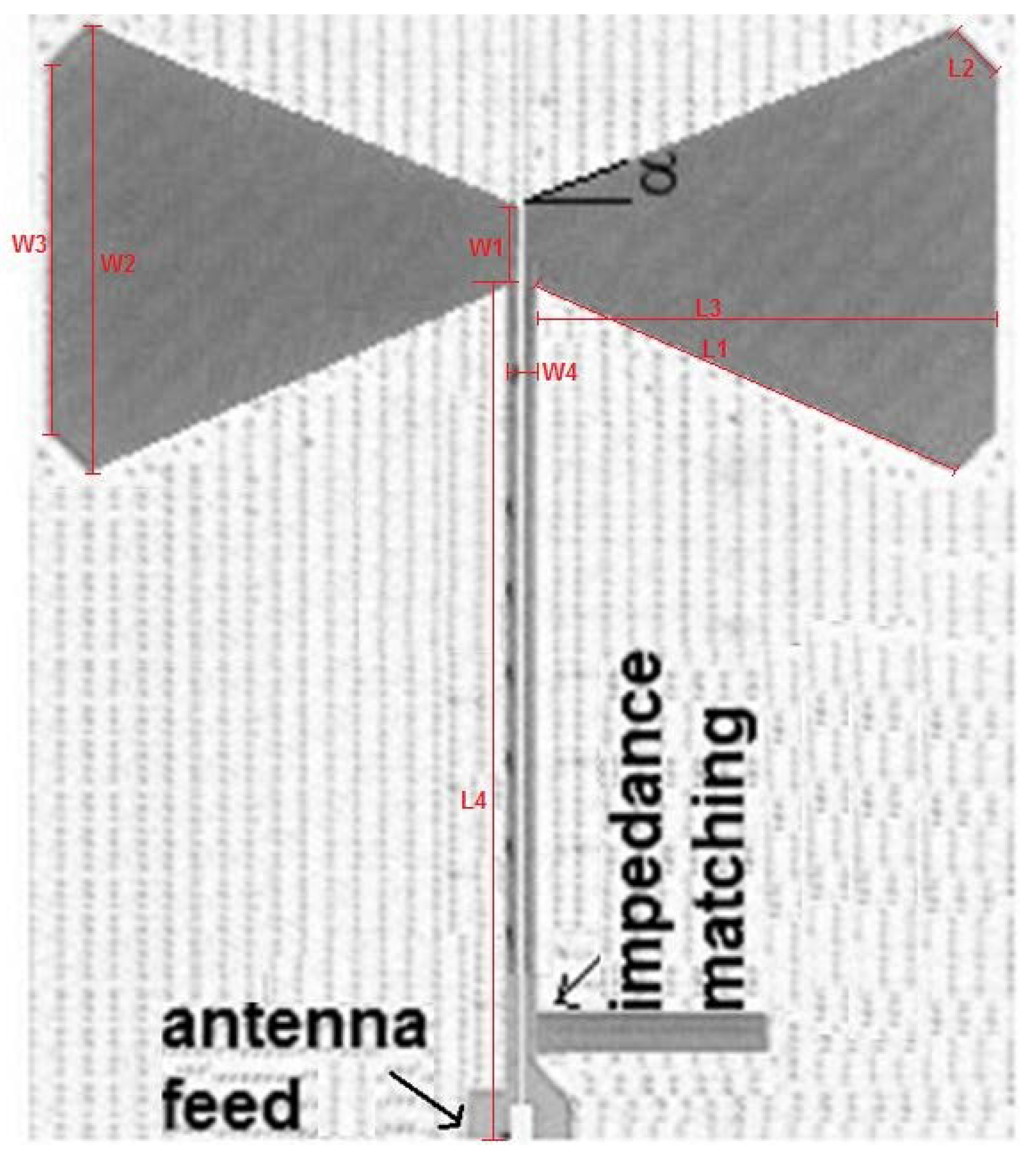
| Parameter | L1 | L2 | L3 | L4 | W1 | W2 | W3 | W4 | α |
|---|---|---|---|---|---|---|---|---|---|
| Value | 350 µm | 50 µm | 350 µm | 637 µm | 60 µm | 330 µm | 275 µm | 20 µm | 25° |
| Area of the rectangle including the antenna | [L4 + 0.5 × (W1 + W2)] × (2 × L3 + W4) = 832 µm × 720 µm = 0.6 mm2 | ||||||||
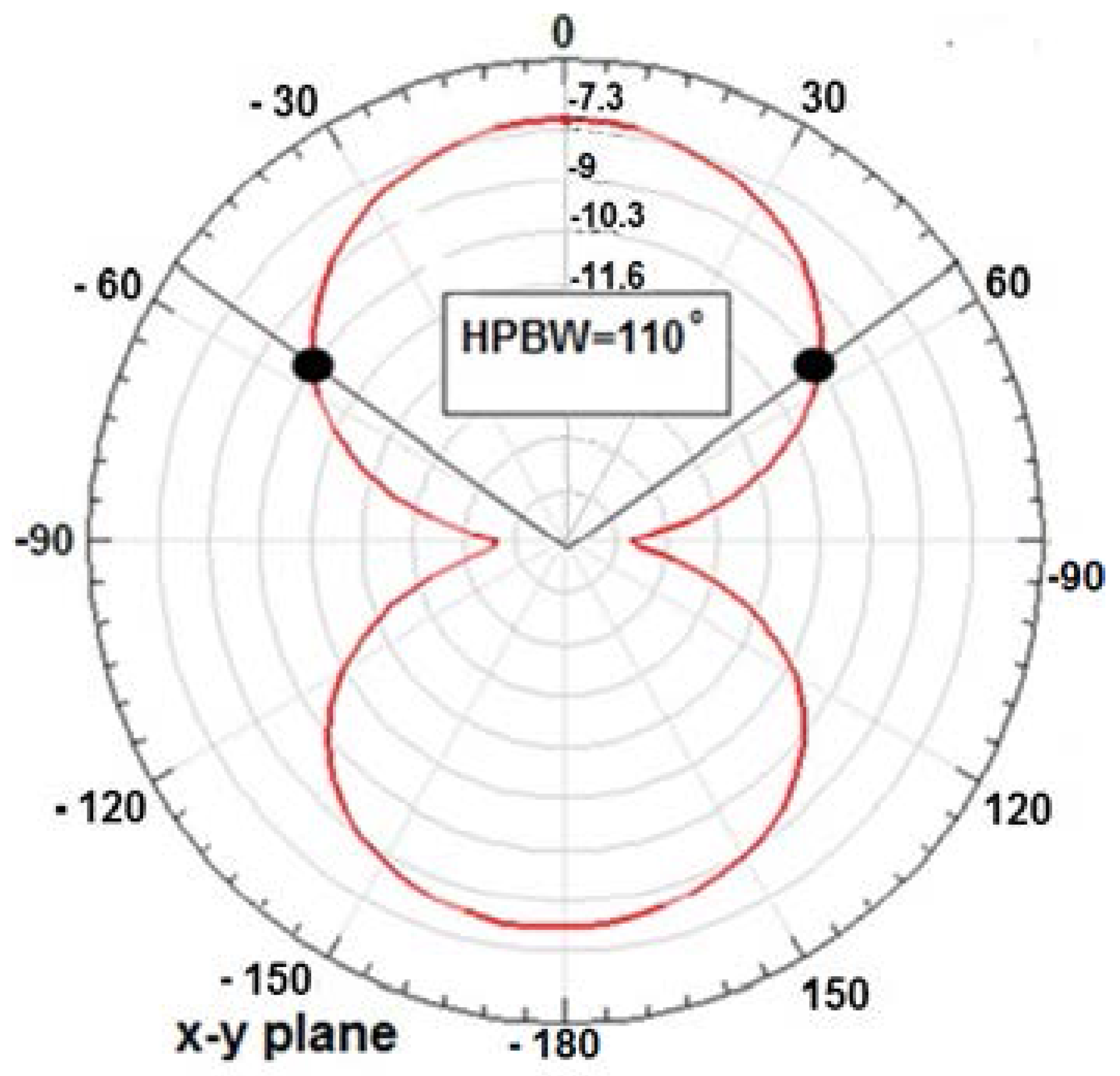
| Antenna | Area, mm2 | Feed/Match Circuit | Gain, dB | HPBWxy | Bandwidth |
|---|---|---|---|---|---|
| This work | 0.512 | Included | −7.3 @ 60 GHz | 110° | 51 to 100 GHz |
| [31,37] | 0.023 | Not included | −26.5 @ 60 GHz | 60° | 51 to 66 GHz |
| [40], Dipole | 375 | Included | 5.8 @ 10 GHz | 65° | 8 to 11 GHz |
| [40], Vivaldi | 300 | Included | 2.8 @ 10 GHz | 85° | 9 to 11 GHz |
| [67] | 156 | Included | 5 @ 60 GHz | 184° | 57 to 64 GHz |
| [79] | 2 | Included | −30 @ 3 GHz | N/A | N/A |
| [83] | 1.4 | Not included | −38.65 @ 60 GHz | 33° | 6 GHz |
© 2017 by the author. Licensee MDPI, Basel, Switzerland. This article is an open access article distributed under the terms and conditions of the Creative Commons Attribution (CC BY) license (http://creativecommons.org/licenses/by/4.0/).
Share and Cite
Gutierrez, F. Design of a Wideband Antenna for Wireless Network-On-Chip in Multimedia Applications. J. Low Power Electron. Appl. 2017, 7, 6. https://doi.org/10.3390/jlpea7020006
Gutierrez F. Design of a Wideband Antenna for Wireless Network-On-Chip in Multimedia Applications. Journal of Low Power Electronics and Applications. 2017; 7(2):6. https://doi.org/10.3390/jlpea7020006
Chicago/Turabian StyleGutierrez, Fernando. 2017. "Design of a Wideband Antenna for Wireless Network-On-Chip in Multimedia Applications" Journal of Low Power Electronics and Applications 7, no. 2: 6. https://doi.org/10.3390/jlpea7020006