1. Introduction
The energy consumption in integrated circuits has been a challenge for designers for many years due to the continuous increase of devices density, speed, and complexity. This challenge is more accentuated in battery-powered devices since low-power devices provide more reliability for the battery life cycle.
Power dissipation in CMOS logic arises from the following sources:
dynamic power dissipation due to the charging and discharging of different parasitic capacitances [
1];
dynamic power dissipation due to a short-circuit current, when both n-channel and p-channel transistors are momentarily on at the same time [
1];
static power dissipation due to a leakage current and a subthreshold current [
1].
In order to minimize power dissipation, low-power considerations should be applied at all levels of design abstraction and design activities. Low-power design techniques and methodologies have been widely reported, each taking place at a very specific stage of the design flow (register transfer level (RTL), logical synthesis or physical synthesis). Examples of such methodologies include dynamic voltage and frequency scaling (DVFS) [
2], parallel architecture [
3], clock gating [
4], and power gating [
5].
During physical design, power reduction techniques are quite limited if compared with other techniques at higher abstraction levels. However, such techniques can have a major impact because some circuits are repeated thousands of times on a chip. Therefore, circuit techniques with small percentage improvements should not be overlooked.
The voltage and frequency in the place and route (P&R) phase are defined as a hard constraint in the specification. The only remaining factors to play with during power optimization are the transition time of signals (slew), the threshold voltage of standard cells, the switching activity of different inputs, the cell placement, and the net routing.
The best known power optimization techniques used in physical design are gate sizing/spacing, buffer/inverter insertion, equivalent pin reordering, logic remapping, critical net re-routing, the use of non-default routing rules, and high-voltage threshold (HVT) cells.
During power optimization, the P&R tools try different methods on each target/cell in order to reduce power (dynamic or leakage). An optimization is accepted if it improves the power without violating the costing criteria, which is a function of the timing (setup and hold), and the electrical design rule constraints (EDRCs) (max transition and max capacitance constraints).
The max transition constraint (MTC) is defined by the designer from the library (.lib) file, which characterizes the standard cells used in the design. This MTC is used by different P&R engines through the physical design flow to provide a clean design layout to the foundry.
In this paper, we will assess the quality of the default MTC definition methodology used by P&R tools, and we will study its impact on power reduction capabilities. We will also evaluate the impact and benefits of redefining the MTC before power optimization phase independently from the library file. By redefining the MTC, we aim to examine the impact of over-constraining and under-constraining a design on power and to find the best trade-off between design constraining and power optimization.
The remainder of this work is organized as follows.
Section 2 presents some basic concepts of power calculation and optimization.
Section 3 provides two case studies.
Section 4 applies the new approach on a wide variety of designs with different technological nodes. Finally,
Section 5 draws the conclusion.
2. The Basic Concept of Power Calculation and Optimization
The energy consumed in an integrated circuit (IC) can be split into two main branches:
A static power dissipation related to the logical states of the circuit. In CMOS logic, the leakage current and subthreshold current are the only sources of static power dissipation.
A dynamic power dissipation, which is caused by the switching activity of the circuit. A higher operating frequency leads to more frequent switching activities in the circuit and results in increased power dissipation. The most significant source of dynamic power dissipation in CMOS circuits is the charging and discharging of capacitances. Sometimes, capacitors are intentionally fabricated to achieve certain non-digital operations. However, most digital CMOS circuits do not require capacitors for their intended operations. The capacitance forms due to the parasitic effects of interconnection wires and transistors, such parasitic capacitance cannot be avoided and it has a significant impact on power dissipation [
6].
As demonstrated in [
6], from the simplified inverter RC network, the dynamic power due to switching current of a CMOS gate (P
sw) can be estimated by Equation (1).
where
Sw is the switching activity of the input,
f is the frequency of operation,
CL is the load parasitic capacitance, and
VDD is the voltage swing across the capacitor.
In [
6], the dynamic power due to short circuit current (P
sc) is estimated by Equation (2):
where
β is the size of the transistors,
τ is the duration of the input signal (transition time), and
Vth is the threshold voltage of the PMOS and NMOS transistors.
Thus, we can reduce power dissipation of a gate by
reducing switching activity;
reducing parasitic capacitance;
reducing transition time;
increasing the threshold voltages of PMOS and NMOS.
The most known circuit level techniques to reduce the dynamic power are gate sizing, equivalent pin reordering, logic remapping, and HVT cell usage.
Gate sizing is very useful in reducing power [
7,
8]. It consists of substituting the big cells that are in the non-timing critical path by smaller gates that satisfy the delay requirement with identical logical function. Such a technique is widely used in the industry for timing, area [
9,
10], and power optimization [
7,
10].
Equivalent pin reordering consists of connecting the input with high capacitance to the net with low switching activity since most combinational digital gates found in a cell library have input pins that are equivalent (e.g., ANDs, ORs, and XORs). Logically equivalent pins may not have identical circuit characteristics, which means that the pins have a different delay or power consumption. Such a property can be exploited for a low-power design [
11].
Net Re-routing: This technique tries to re-route nets with high parasitic capacitances in a lower congested area to reduce the parasitic capacitance caused by neighboring wires [
12,
13].
The use of HVT cells in non-timing critical paths: A leakage current is inversely exponential to V
th; therefore, by using high-threshold voltage cells, the amount of leakage current and hence the leakage power is reduced [
14,
15].
During the physical design phase, the above techniques are used to optimize power consumption depending on the stage of the design. For example, power optimization at placement stage aims to optimize the placement from a power point of view, which implies the downsizing or remapping of big cells on sub-critical paths [
16,
17]. Similarly, in CTS (clock tree synthesis) stage, the clock tree quality plays a very important role in power reduction because it is the longest net and drives the biggest load in the circuit (all the synchronized elements). Many considerations are taken to reduce power dissipation in the clock network [
18].
At the routing stage, most power optimization techniques deal with wires and via capacitance and resistance reduction. Some non-default routing rules and long net re-routing techniques are used for this purpose [
19].
After routing is complete, new timing, electrical, and routing design rule violations (DRVs) appear. The timer at this stage deduce the coupling noise between metal lines and provide more accurate timing and power pictures, so another round of optimization is needed to clean the design [
20].
3. Max Transition Variation Impact on Power Optimization (Case Study)
The transition time is the time needed for a signal to pass from 10% to 90% or from 20% to 80% of its final state. The delay of a cell can be deduced from the standard cell library, it is a function of input transition time and output capacitance load. During the cell characterization phase, the library’s developers calculate using the cell’s SPICE models, the cell’s delay, and the output transition for each input transition and output load combination.
Additionally, they define the max transition and max capacitance, which represent the limits of where the cell is characterized. Those values are used as constraints by P&R tools to extract the delay and power of the design. Users can also impose new max transition or max capacitance constraints; in this case, the P&R tools use the most pessimistic value between the user-defined values and the library values.
When applying a max transition constraint on a design, the tool considers all transitions greater than this max transition as violations and tries to fix them by upsizing the drivers, downsizing the loads, or inserting buffers to split the loads. If the tool is over-constrained, it will see many violations and will try to fix them, which will lead to upsizing and buffer insertion of many cells. Under-constraining the tool will also hide certain targets where downsizing is possible. Both scenarios impact power reduction capabilities.
Most of the published research on power reduction techniques at the circuit level adopt a bottom-up methodology and treat the power issue on a gate level [
7,
8,
9], which means that they prove the effectiveness of a technique on a design with few gates and then try to generalize on multi-million gates designs. In some cases, if we apply such a technique on a gate, the power and timing of neighboring gates may be impacted, as presented in [
8].
By examining the global picture of the physical design flow, we noticed that global constraints that affect power optimization, such as the MTC, are left to their default values. Usually, the MTC is defined based on the timing library file (.lib) by taking the average max transition of all lib cells’, or may be defined by the user in the standard delay constraints file (.sdc), and the tool takes the most pessimistic value between the user-defined and lib-defined MTC values. This value might not be optimal for power optimization and could over-constrain or under-constrain the design.
This section will explore the impact of changing MTC on power reduction capabilities on two different designs, with different sizes and technological nodes. It will first provide a P&R flow used to run the experiments and will then examine the results.
With the aim of evaluating the MTC variation impact on power optimization, we developed the following flow (Flow 1):
| Flow 1: Check MTC Impact on Power Reduction. |
| 1: For Tran ∊ {0… MTCD} do |
| 2: Read Design Database |
| 3: Enable power in all corners |
| 5: Set MTC MTCD |
| 4: Estimate power (Initial value) |
| 5: Set MTC Tran |
| 6: Optimize Power |
| 5: Set MTC MTCD |
| 7: Estimate power (Final value) |
| 8: Evaluate timing impact (setup and hold) |
| 9: END for |
We developed a flow (Flow 1) that varies the max transition constraint (MTC) and evaluates the power improvement after its optimization. First, we set the range of MTC values to explore between 0 and MTC default (MTCD). Then, we loaded the design database, which consists of the netlist, the timing and technology library files, and the timing constraints in Nitro SoC. After that, we enabled the power in all of the design’s corners and estimated the initial power and timing values given by the default MTC. We then applied the max transition constraint (MTC) on the design. We made a pass of power optimization using Nitro SoC optimization engine, and we reset the MTC to MTCD again for comparable results. Finally, we calculated the power reduction and the timing impact for the specific MTC applied using Nitro SoC’s static timing analysis (STA) and power estimation (PE) engines.
3.1. Test Case 1 Results
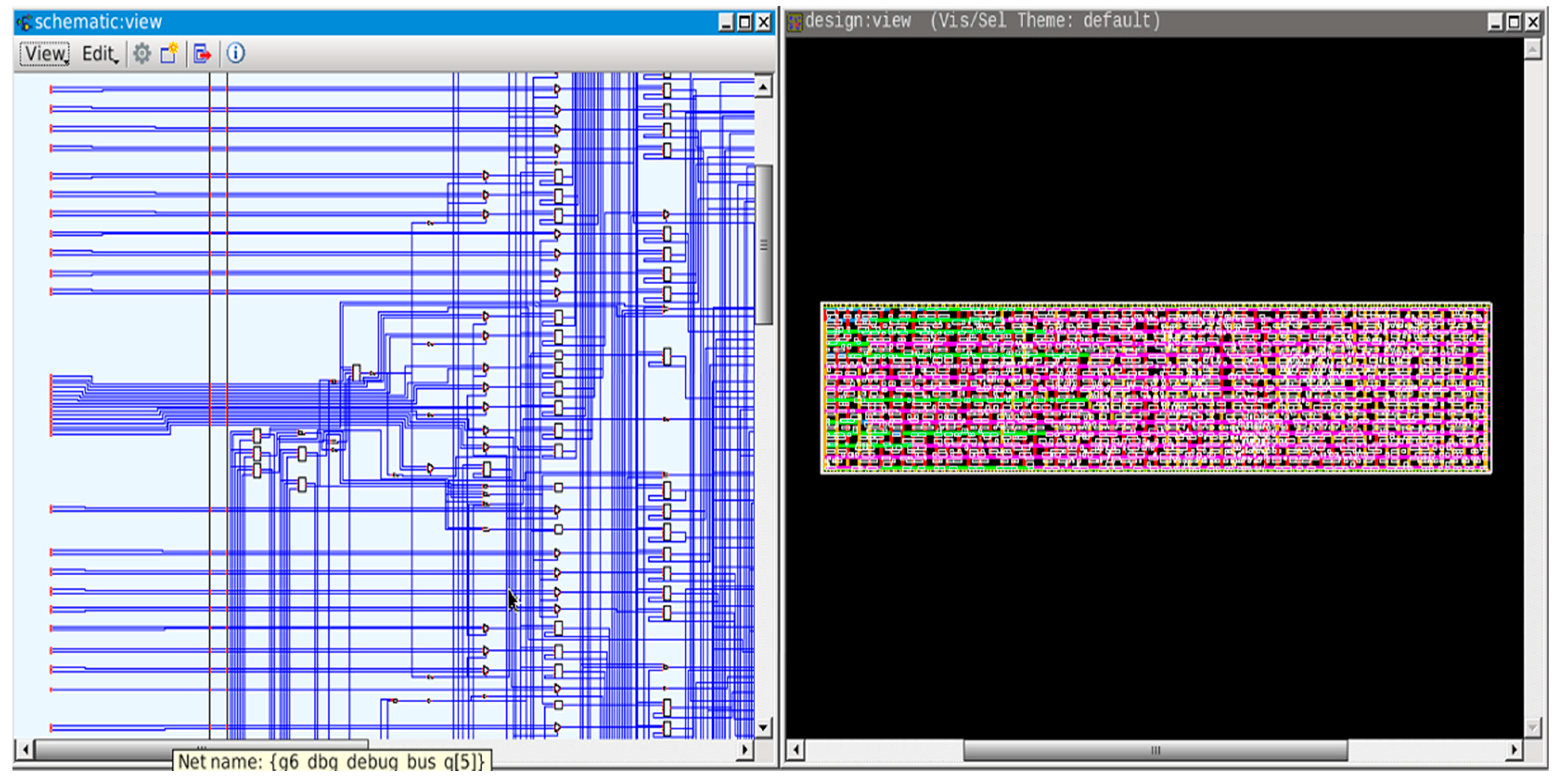
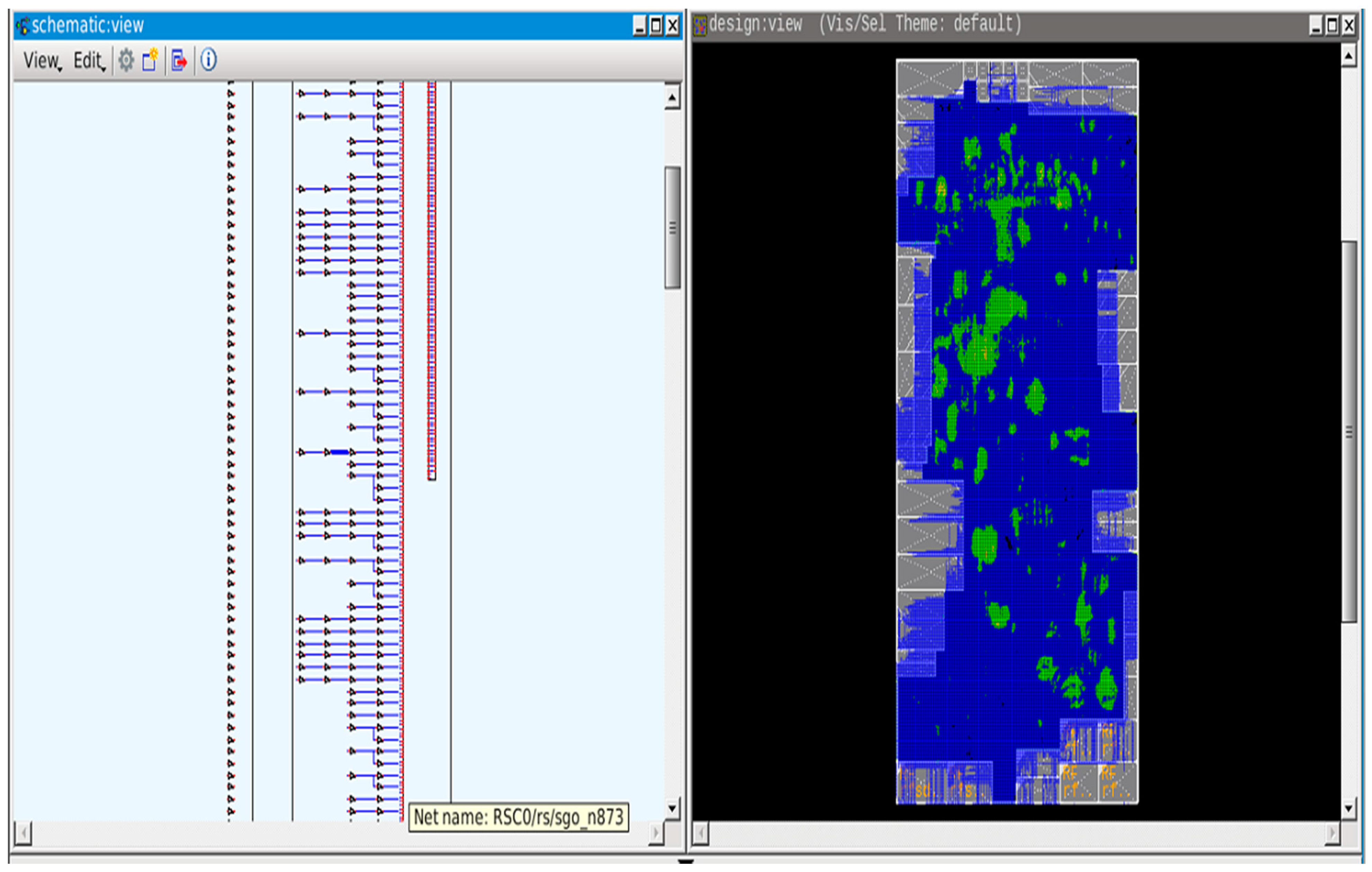
We applied Flow 1 on Test Case 1 (
Figure 1), the characteristics of which are summarized in
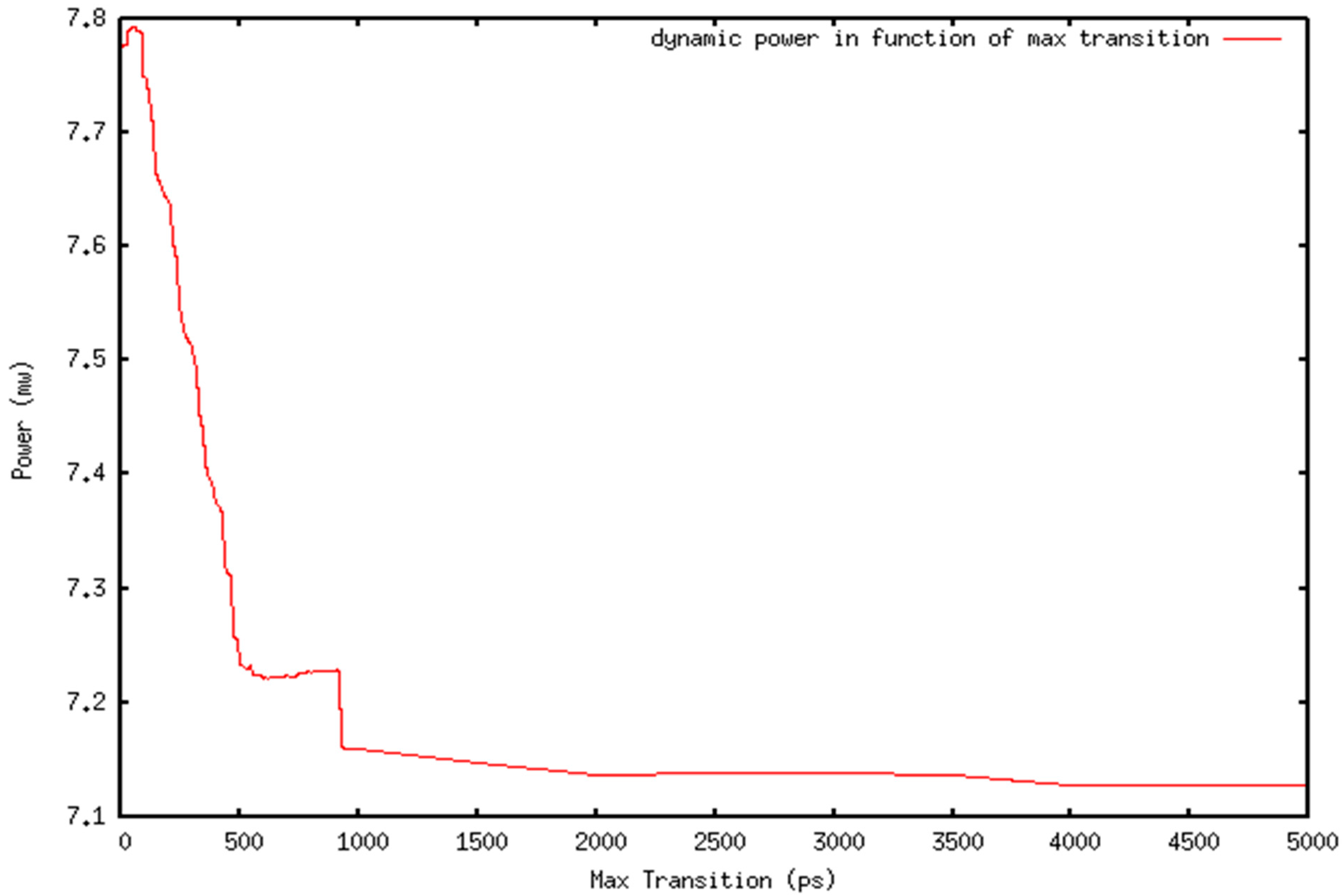
Table 1. We evaluated for an MTC interval of [0 ps–5000 ps], the corresponding power reduction achieved after optimization. The graph in
Figure 2 summarizes the results. We noticed that the power dissipation is reduced rapidly as MTC increases until 1000 ps. Then, it still decreases slowly until it reaches 4000 ps. Then, the power reduction is constant. This means that, in order to achieve the optimum power reduction, the MTC should at least be equal to this threshold value. Constraining the design with an MTC less than this threshold value will result in a sub-optimal power dissipation reduction.
3.2. Test Case 2 Results
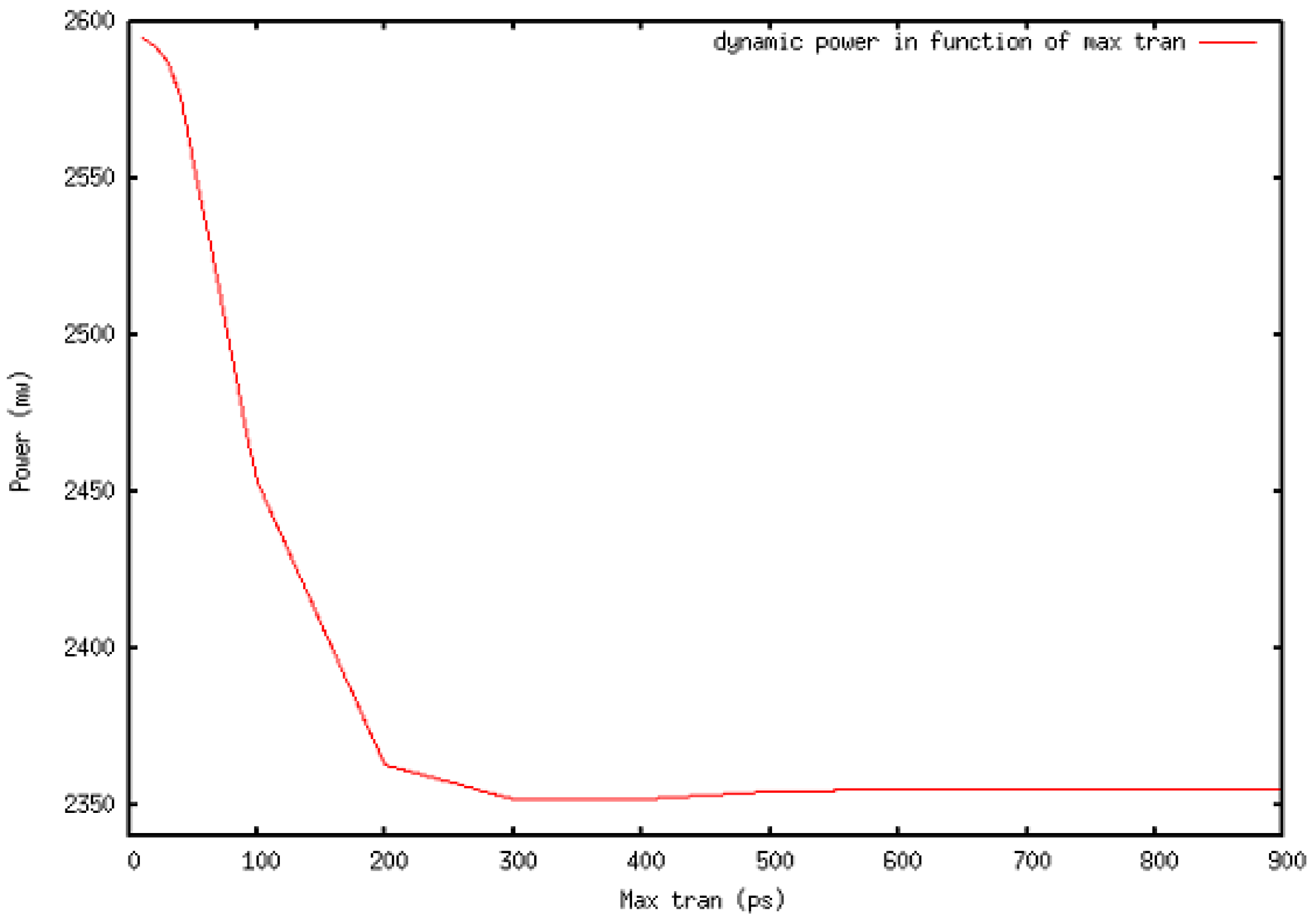
We repeated the same experiment on Test Case 2 (
Figure 3), which has the characteristics summarized in
Table 2. We estimated for the same MTC interval as Test Case 1, the corresponding power achieved after optimization. The graph in
Figure 4 summarizes the results. We noticed that the power dissipation is reduced as MTC increases up to a given threshold (between 200 and 400 ps) and then starts increasing again as MTC continues to rise, which means that for certain MTC intervals the power reduction is optimal and that, by increasing the MTC beyond this interval, we under-constrain the design and hide certain areas of power reduction. Moreover, by decreasing the MTC below this interval, we over-constrain the design, and this results in sub-optimal power reduction.
4. Experimental Results
The two motivational examples presented in
Section 3 provide evidence that the default MTC value is not optimal for power optimization and prove the existence of another MTC range where power optimization achieves the best power reduction gain. However, to detect this MTC interval, many runs are needed, which is runtime- and resource-consuming. Therefore, in order to reduce the runtime and the used resources, we proposed a new algorithm in which we adopted a dichotomous approach, described in Algorithm 1. The algorithm automatically detects the best MTC value needed to attain better power reduction results.
The algorithm first loads the database (file.db), which includes the synthesized netlist, the liberty files, and the technological files. In a second step, it detects the default MTC value in the design (MTC
d), then it runs the power optimization and assesses the reference power improvement value (Power
d) and the timing impact. Using a dichotomous approach, it starts to split the interval between MTC
d and 0 and calculates the power optimization gain (Power(i)); based on the results, it repeats the same operation in the sub-interval that provides the best power reduction until the interval size is less than a given threshold value. At the end, it returns the MTC sub-interval that provides the best power reduction results.
| Algorithm 1: Optimal MTC Detector |
| 1: Procedure MTCDechotomy () |
| 2: Load the Data Base (file.db) |
| 3: MTCd ← Default MTC value in the design |
| 4: Powerd ← Run_power_optimization (MTCd) |
| 5: Estimate reference power reduction and timing impact |
| 6: Initialize the first 3 MTC values |
| 7: MTC(0) ← 0 |
| 8: MTC(1) ← (MTC(0) + MTC(2))/2 |
| 9: MTC(2) ← 1000 × MTCd |
| 10: While (MTC(i) − MTC(i − 1) > Threshold) do |
| 11: Power(i) ← Run_power_optimization(MTC(i)) |
| 12: Reset the MTC to default value (MTCd) |
| 13: Estimate power reduction and timing impact |
| 14: If Power(i) < Power(i − 1) then |
| 15: MTC(i) ← (MTC(i − 1) + MTC(i − 2))/2 |
| 16: Else |
| 17: MTC(i) ← (MTC(i − 2) + MTC(i − 3))/2 |
| 18: End if |
| 19: End while |
| 20: Return Trans value that gives the min power |
| 21: End procedure |
Applying Algorithm 1 on Test Case 2 produces the results in
Table 3. The results indicate that the power varies between 2403 mw when MTC is less than 268, which means that, by choosing an MTC <268, we are over-constraining the design. Additionally,
Table 3 indicates that an optimum MTC value is between [251.7–268.5] ps, which corresponds to a power between [2353.2–2352.1] mw. Relaxing the MTC with a value greater than 268.5 means that we are under-constraining the design and that a sub-optimal value, such as MTC = 1074.0, will result. By adopting this dichotomous approach, we were able to detect a good transition value in a few iterations (8 in Test Case 2).
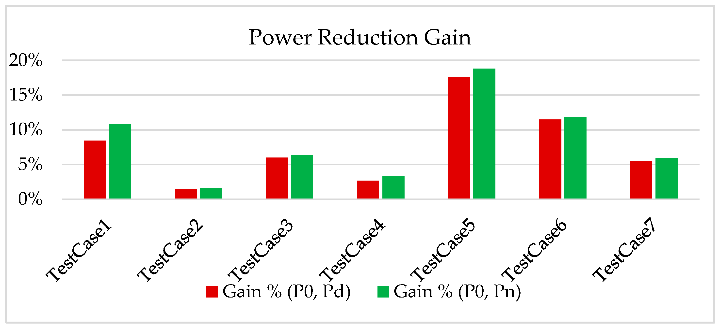
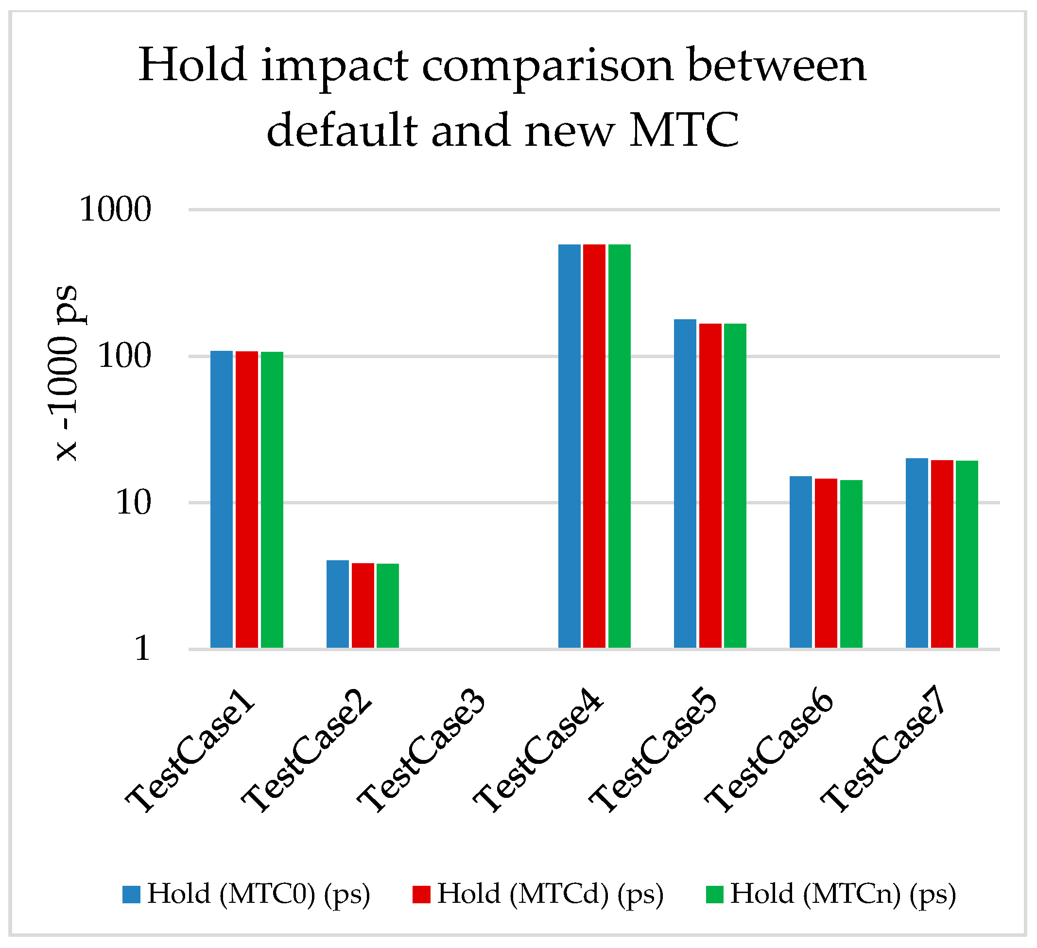
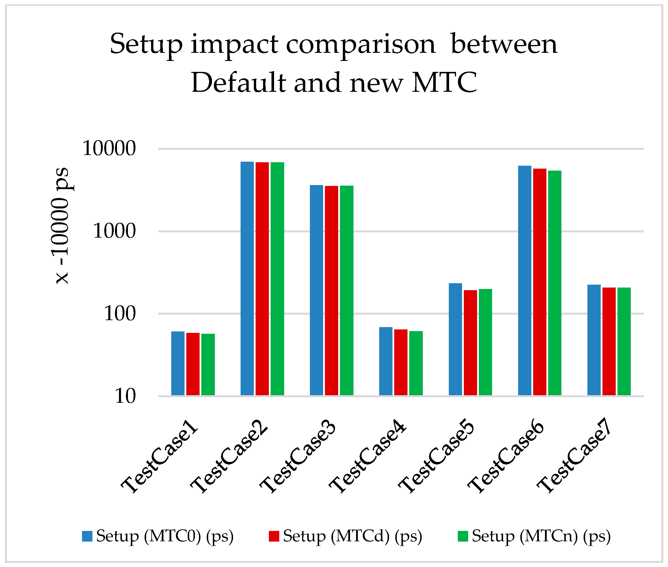
We applied Algorithm 1 on a wide variety of designs, with different sizes and technological nodes using Nitro SoC’s P&R tool. For each design, we reported the initial power (P0) and the default MTC (MTCd) values, ran the power optimization for this default MTCd, reported the final power reduction (Pd (MTCd)), and calculated the default power gain (Gain % (P0, Pd)). After that, we used Algorithm 1 to detect the optimal MTC value (MTCn) and applied it, ran power optimization, and reported the new power reduction (Pn (MTCn)) and the new power gain (Gain % (P0, Pn)). We also reported the timing (setup and hold) for both the default and the newly generated MTC.
We deduced from the results shown in
Table 4 and
Figure 5 that, with the default MTC, the average power gain is 38.3%, while it reaches 43.3% with the newly generated MTC. Additionally, we noticed that the timing is better in most cases for both setup and hold (
Figure 6 and
Figure 7).
The power gain is mainly due to the decrease in short-circuit time, which leads to the decrease in internal power, as per Equation (2). The gain in the setup timing is because of the signal speedup, since the MTCn is smaller than the MTCd in all test cases. The gain in the hold timing is a side effect of the power optimization, as one of the techniques of power optimization is to downsize the cells in the sub-critical paths, which automatically leads to improvements in the paths with hold violations.
In the experiments, we noticed that, by applying MTCs that are too small, we are over-constraining the design. Over-constraining the design forces the optimization engine to reject power improvement solutions due to a max transition-costing violation, which means that, if a solution improves power but violates the MTC, it will be rejected. A large MTC, on the other hand, causes a power increase due to increased short-circuit power, which is a linear function of the transition time. By under-constraining the MTC, we are allowing the design to have large transitions—hence the short circuit power, which is an important component of the dynamic power. Therefore, there is an optimum value in between, which we can find using our algorithm (Algorithm 1).
5. Conclusions
By evaluating the effect of max transition constraint on power optimization over various designs and technological nodes, we demonstrated experimentally that, in order to reduce the power consumption of a System on Chip (SoC) optimally, one should evaluate different values of max transition to well constrain the design before starting power optimization. We also showed that, by adopting this method of max trans evaluation, the gain in power reduction reaches 2.35% in some designs.
The algorithm presented in
Section 4 was applied on more than 100 designs, and the obtained results confirmed that careful attention should be taken when constraining a design to drive physical design tools, such as Nitro SoC from Mentor Graphics, and to attain the optimum power reduction.
6. Perspectives
This paper proved the existence of a good MTC value (MTCn) that gives better power reduction results, which is different from the default MTC (MTCd). More work can be done to reduce the runtime of finding the MTCn value by using more efficient analytical techniques other than the dichotomy approach adopted in this paper. Additionally, another dimension may be explored by studying the relationship between the design node, size, structure, and MTC, which may lead to a direct method or equation to find the best MTC without running any experiments.


