A Low-Power Active Self-Interference Cancellation Technique for SAW-Less FDD and Full-Duplex Receivers


Department of Electrical, Computer and Biomedical Engineering, University of Pavia, 27100 Pavia, Italy
*
Author to whom correspondence should be addressed.
J. Low Power Electron. Appl. 2017, 7(4), 27; https://doi.org/10.3390/jlpea7040027
Submission received: 29 September 2017
/
Revised: 4 November 2017
/
Accepted: 10 November 2017
/
Published: 13 November 2017
(This article belongs to the Special Issue Low-Power Electronic Circuits for Monolithic Smart Wireless Sensors)
Abstract
:An active self-interference (SI) cancellation technique for SAW-less receiver linearity improvement is proposed. The active canceler combines programmable gain and phase in a single stage and is co-designed with a highly-linear LNA, achieving low noise and low power. A cross-modulation mechanism of the SI canceler is identified and strongly suppressed thanks to the introduction of an internal resistive feedback, enabling high effective receiver IIP3. TX leakage of up to −4 dBm of power is suppressed by over 30 dB at the input of the LNA, with benefits for the entire receiver in terms of IIP3, IIP2, and reciprocal mixing. The design was done in a 40 nm CMOS technology. The system, including receiver and active SI canceler, consumes less than 25 mW of power. When the canceler is enabled, it has an NF of 3.9–4.6 dB between 1.7 and 2.4 GHz and an effective IIP3 greater than 35 dBm.
Keywords:
blocker; cross-modulation; distortion cancellation; diversity; FDD; full-duplex; IIP3; SAW-less; self-interference1. Introduction
The evolution of mobile communication technologies ranging from GSM to the future 5G has continuously required increased data rates and quality of service and, in general, the miniaturization of devices and costs reduction. Off-chip Surface Acoustic Wave (SAW) filters are typically used to reject out-of-band interferers and Self-Interference (SI) signals (or transmitter leakage) but cause a significant form factor burden, even more so when the device operates over a large number of bands and uses multiple antennas. Also, the reconfigurability of receivers with SAW filters is difficult to achieve. Much attention is now focused toward SAW-less receivers, and several architectures have been proposed that are capable of tolerating large SI signals. There are various challenges that arise with the SAW-less receivers. For instance, when operating in Frequency Division Multiplexing (FDD) mode, where the transmitter (TX) and receiver (RX) operate simultaneously in different frequency bands, the TX leakage could inter-modulate with the out-of-band (OOB) blockers, thereby resulting in in-band third-order and second-order intermodulation, as well as generate reciprocal mixing. Furthermore, wideband TX noise leakage in the receive band can severely degrade receiver sensitivity [1]. Transceivers operating in Full Duplex (FD) mode, where the TX and RX overlap in time and frequency, are inherently SAW-less and pose an even greater SI challenge since a very large (in the order of 110 dB [2]) TX-RX isolation must be ensured, which also requires very high in-band linearity.
In a single-antenna transceiver, a circulator can be used to provide isolation between transmitter and receiver. Alternatively, isolation can be achieved using separate antennas for transmitter and receiver. This basic isolation can be improved using RF cancelation architectures, either based on an RF canceller [3,4] or on an auxiliary transmitter [5]. The use on an auxiliary transmitter allows to achieve very high cancellation levels and bandwidths even in the presence of strong power amplifier nonlinearity. However, it does not address the issue of transmitter noise leaking into the receiver. With a typical TX noise level in the order −160 dBc/Hz [6], if the transmitter leakage is sufficiently low (e.g., −20 dBm or less), this is not a major concern. If instead the transmitter leakage approaches 0 dBm, sensitivity degradation becomes large, and an RF canceller is potentially more attractive. A major issue of RF cancellation is given by the limited cancellation bandwidth, which results from the substantial delay (in the order of ns) between the TX signal and the SI at the RX input. Several board-level demonstrators have been implemented using off-the-shelf components, reporting strong cancellation levels over broad bandwidths. In [3], using a circulator showing multiple coupling paths with delays from 0.5 ns to 2 ns, 33 dB cancellation over 20 MHz and 18 dB cancellation over 100 MHz was reported using an RF canceller based on a two-tap delay line followed by programmable vector modulators under self-adaptive control. In [4], a three-tap RF canceller achieved 41 dB cancellation over 80 MHz bandwidth. Moving from the above mentioned solutions—based on off-the-shelf components mounted on a printed circuit board or connected using cables—to fully-integrated solutions, several implementation challenges related to component integration (e.g., RF delay lines) and dynamic range limitations are faced, typically leading to much smaller form factors but inferior cancellation levels and bandwidth. Prior works have proposed several integrated architectures to substitute the off-chip filters with tunable integrated solutions. Early works have advocated the use of passive hybrid transformers (HT) [7,8]. The HT allows us to connect TX and RX to the antenna port while ensuring isolation between TX and RX. The main limitation of HTs is that 3 dB loss is incurred between the TX and the antenna as well as between the antenna and the RX, degrading power efficiency and sensitivity. Furthermore, in typical HT configurations, the TX signal appears as a large common-mode signal at the LNA input due to parasitic coupling capacitors. A large common-mode leakage could saturate the LNA. The common-mode leakage could also cross-modulate with a jammer, thereby degrading the receiver linearity. The noise of the broadband common-mode signal could also appear at the RX signal thereby degrading the receiver sensitivity. The author [7] proposed a differential HT that would cancel out this common mode leakage signal, but this would nearly double the power consumption and area and additional loss from the balun that is needed to convert the transceiver differential signal to single ended at the antenna port. In [8], the issue of common-mode coupling due to parasitic capacitor was not addressed. The author relied on the linearity of the LNA design, which tolerated blocker of up to −15 dBm. Due to the frequency variability of the antenna impedance, transmitter-to-receiver isolation is in the order of 50 dB for a signal bandwidth of 6 MHz as illustrated on the TX/RX isolation plot. Other single antenna self-interference cancellation works have also been proposed in [9,10,11,12,13,14,15,16].
The use of a dual antenna architecture can significantly relax the design challenges since the limited coupling provides isolation between TX and TX without incurring any signal loss. However, the usual isolation between a pair of antennas in a mobile device is typically in the order of 20–30 dB [17] in contrast to a HT-based transceiver. Hence, a highly linear and tunable self-interference canceler (for FDD and FD) is required to further attenuate the TX leakage.
Other works have advocated the replacement of the off-chip filters with SI cancellation techniques [11,18] or the use of N-path filters [13,19] to either achieve FDD or FD operations.
The SI canceler must have variable gain and it must be able to track and adjust its phase over the entire 360° phase shift. In the two-point cancellation architecture proposed in [18] the LNA is based on the noise-cancelling approach and is able to tolerate up to 2 dBm TX leakage power while achieving high effective OOB IIP3. However, the TX leakage is effectively cancelled only after down-conversion and recombination between common-gate and common-source paths. As a result, it does not address SNR degradation due to IIP2 and reciprocal mixing. An N-path filter based canceler, which was designed for both FDD and FD applications has been proposed in [20] using dual antenna architecture. The use of passive mixer switches in the N-path filter results in large power dissipation and the N-path LO is prone to reciprocal mixing. With 30 dB isolation between the TX and RX, up to −4 dBm TX leakage power was tolerated by the filter. However, the effective IIP3 is only improved by 10 dB for more than 25 dB of leakage suppression, which highlights an intrinsic linearity limitation from the canceler. A low-power mixer-first receiver with passive mixer based self-interference cancellation is proposed in [21] for dual antenna FD. It handles a SI of up to −10 dBm and 25 dB of suppression is achieved over a limited bandwidth. Moreover, the effective IIP3 improvement is limited. The SI cancellation is done after the mixer, hence, reciprocal mixing is an issue for this architecture. A passive canceler based on an analog FIR filter in the RF side and another FIR filter in the baseband was proposed by [22] for dual antenna FD systems. The FIR filter taps consist basically of a true-time-delay circuit, a buffer and a variable gain amplifier. A 40 MHz cancellation bandwidth was achieved over a 50 dB leakage cancellation, however at the expense of high power consumption and noise degradation which scales with the number of FIR taps.
This paper describes an active SI cancellation technique for a SAW-less diversity receiver, extending the conference publication [23]. In this work, the design is extended including the down-conversion mixers and baseband trans-impedance amplifiers (TIAs). Furthermore, an expanded analysis of the system requirements, performance analysis and design details are reported. The active canceler was designed to adjust both its gain and phase to produce a signal that adds destructively to the SI signal, acting as a programmable vector modulator. The use of the SIC in the dual antenna system further increases the TX-RX isolation from below 30 dB to above 50 dB, as obtainable in a SAW-based system. This approach therefore, improves the effective receiver linearity. It was shown in [17] that in a typical multi-antenna handset configuration, the group delay of the SI path due to antenna coupling is typically in the order 2–3 ns and that, this limits the achievable cancellation to about 20 dB over a bandwidth of 10 MHz. Improved cancellation bandwidth may be achieved integrating an analog delay line in the canceller as proposed in [22] or using an additional digital cancellation path, as advocated in Figure 1, due to space limitations issues related to limited cancellation bandwidth as a result of larger antenna group delay are left for future work. This paper is organized as follows: Section 2 describes the system architecture and the system level requirements of the receiver chain. Section 3 describes the circuit implementation of the active SI canceler and the receiver chain. Section 4 discusses the simulation results. Section 5 concludes the paper.
2. System Architecture and Requirements
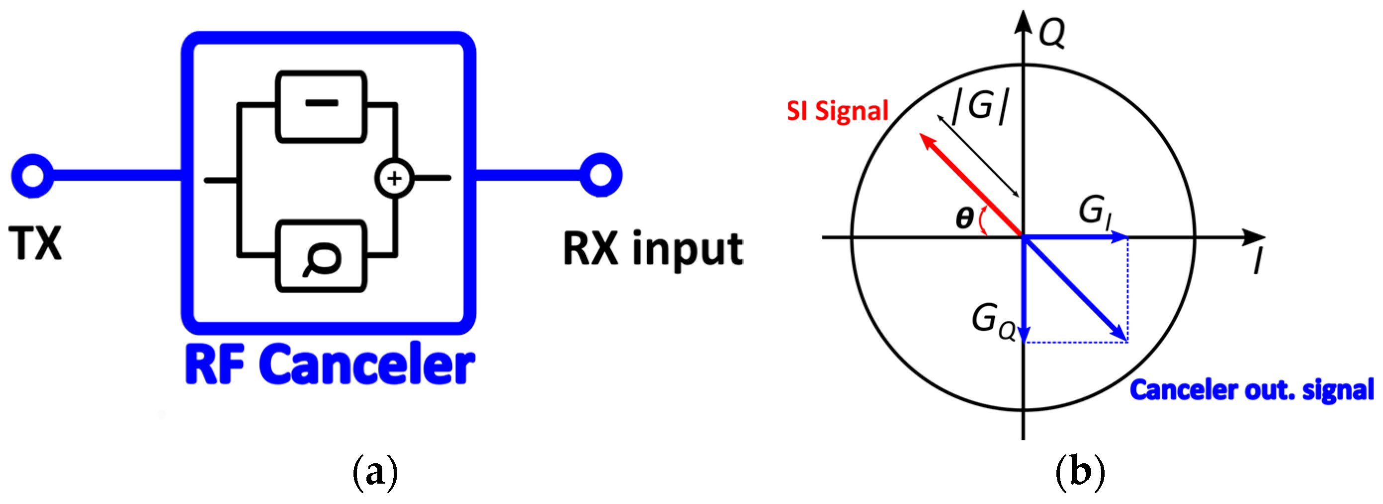
The proposed receiver with active SIC is shown in Figure 1. The analog RF canceler senses the TX signal from the PA and cancels out the modulated TX leakage signal at the input of the LNA. An auxiliary receive path is used to sense the broadband TX noise and cancel it out in the digital domain, as reported in [24]. Digital cancellation also allows to improve the cancellation level provided by the RF canceller and to extend the cancellation bandwidth. This issue however, is not covered in this work due to space limitations. The choice of cancelling the leakage signal at the LNA input relaxes the stringent linearity requirement of the entire receive chain, including the LNA, both in terms of IIP2 and IIP3, and reciprocal mixing is strongly reduced. However, the noise of the canceler is directly seen at the receiver input port and, therefore, the canceler must be designed with lower noise contribution. Canceling the SI after the LNA, e.g., as proposed in [25], could result in LNA clipping and receiver desensitization at large SI levels. Similar considerations apply to the SI architecture proposed in [22], where SIC is carried out at baseband. Furthermore, the introduction of a down-conversion mixer in the SIC path may cause reciprocal mixing with the LO phase noise, further increasing the RX noise.
2.1. Receive Chain
2.1.1. Requirements for FDD
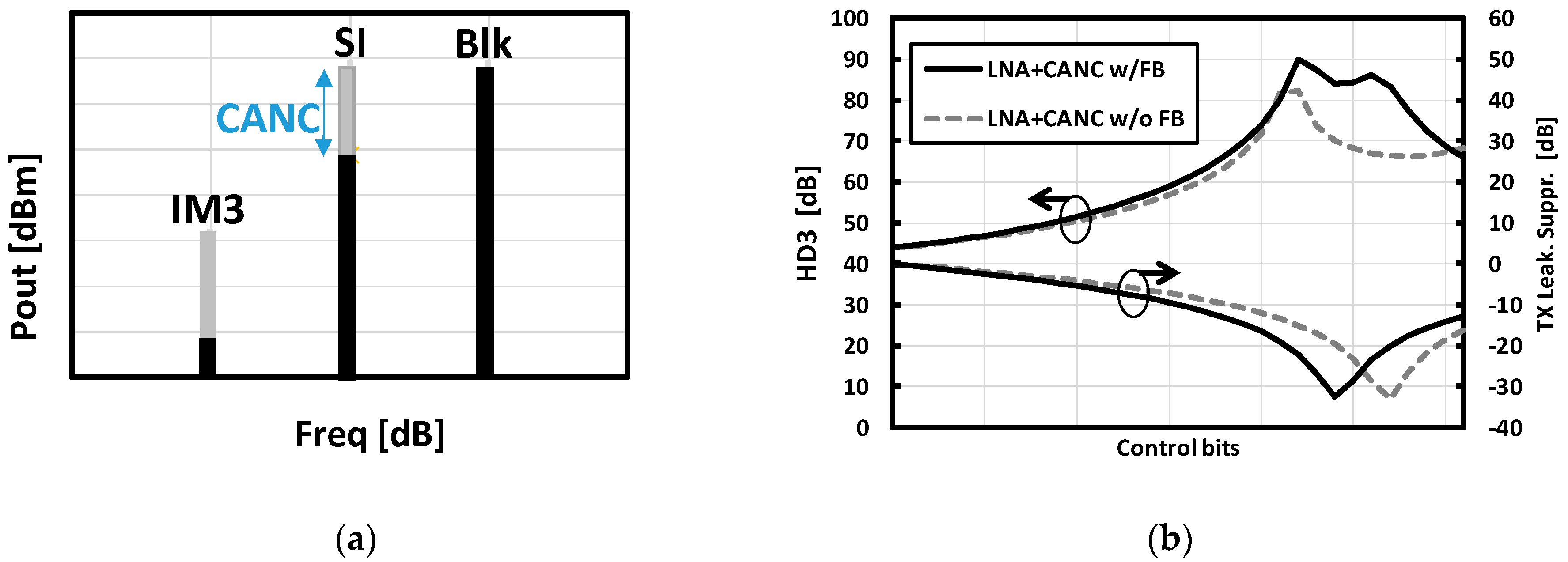
In a dual antenna mobile terminal, the isolation between TX and RX antennas can be around 20 dB to 30 dB [17]. Here, we assume 25 dB TX-RX antenna isolation as a typical value. For the FDD scenario, we consider as a reference 4G LTE band 2 with 20 MHz channel bandwidth [26]. With the maximum TX power of 23 dBm, the maximum TX leakage signal arriving at the RX antenna is −2 dBm. Removing external filters in front of the receiver, OOB blockers as high as −15 dBm may be present at the receiver input together with the −2 dBm TX leakage. This can cause strong in-band intermodulation if the receiver IIP3 is not sufficiently high. In the presence of a strong OOB blocker, the receiver sensitivity of −92 dBm (for QPSK modulated wanted signals) can be degraded by 9 dB for 20 MHz channel bandwidth [26]. Considering a signal-to-noise ratio of −1 dB for QPSK, the maximum noise + distortion level is −82 dBm. Assuming, pessimistically, that the receiver has the maximum allowed noise figure of 9.8 dB, which barely meets the sensitivity requirement, the maximum third-order intermodulation level is −82.6 dBm. Hence, in the worst case, i.e., when the OOB blocker appears at a frequency offset from the receiver that is exactly twice the TX-RX frequency spacing, the effective receiver IIP3 (as defined in [18]) should be larger than −2 dBm + (−15 + 82.6)/2 = 31.8 dBm. Such a high value is nearly impossible to achieve using standard LNA design techniques and represents a challenging target even for SIC FDD receiver architectures. Assuming an RF SIC of 20 dB in front of the receiver, the receiver IIP3 requirement is decreased by the same amount to a more feasible value of 11.8 dBm. Nonetheless, the nonlinearities of the canceller are also very important and can easily become the bottleneck for the entire receiver. To illustrate this issue, we refer to Figure 2.
The canceler sees the large TX signal at the input (VTX) and a large blocker signal (VBK) at the output. This causes two types of nonlinearities. First, due to the nonlinear canceler gain, the TX signal generates intermodulation products in the vicinity of the TX band. In FD mode, since TX and RX bands coincide, this is the main nonlinearity mechanism affecting the receiver effective IIP3. Second, due to the canceler limited reverse isolation, its output signals, including its nonlinear products, are modulated by the blocker at the canceler output (i.e., at the receiver input). This creates cross-modulation products between the TX signal and the blocker, that degrades the SIC receiver effective IIP3 in FDD mode. We express the canceler characteristic using a Taylor series expansion as follows:
and we assume that the TX signal is given by two tones () and the blocker is CW (). The two nonlinear mechanisms described above generate two distinct 3rd order nonlinear products: the intermodulation between the TX input tones (Vo,IM3) and the cross-modulation between the TX tones and the blocker (Vo,XM3).
To mitigate the cross-modulation product, which is the limiting factor in FDD mode, a feedback path (β) is introduced from the canceler output to its input. Hence, the canceler input signal becomes , and an additional cross-modulation term is generated as follows:
Setting the feedback factor properly (β = λα2/α3) the two cross-modulation products cancel each other: . Notice that since both the canceler gain (α1) and the feedback factor (β) are small, the loop gain is much smaller than one and hence no stability issue arises.
2.1.2. Requirements for FD
In full duplex transceivers, the simultaneous transmission and reception of signals at the same time and frequency makes self-interference cancellation an even greater challenge. For this reason, FD transceivers typically target communication links over shorter distances, where lower transmitted power levels and receiver sensitivities can be tolerated. In this work, we envision a dual antenna FD system with a transmitted power of 10 dBm and a sensitivity of −82 dBm. Assuming 25 dB antenna isolation, the TX leakage is −15 dBm and the total cancellation needed to have the SI below the RX sensitivity is (82 − 25 + 10 =) 67 dB. The use of an RF canceler would not be able to achieve this cancellation due to nonidealities and low resolution constraints in the canceler design. Assuming 27 dB of cancellation in the RF domain, the further 40 dB would be done in digital domain (e.g., using an auxiliary path). Notice that both the TIA and the ADC must have a dynamic range (DR) greater than 40 dB. The effective receiver in-band IIP3 requirement can be computed assuming a 3 dB sensitivity degradation when the transmitted power is maximum, i.e., −15 + (−15 + 82)/2 = 18.5 dBm.
2.2. Self-Interference Canceler Architecture
Prior works have proposed different ways of generating the SI cancellation signal. In [18], the SI canceller consists of a variable phase shifter followed by a programmable gain amplifier. Cascading the two functions degrades noise and linearity performances and raises the power consumption. An alternative solution to generate the cancellation signal requires the use of a passive RC-CR quadrature splitter followed by two programmable gain amplifiers [27]. A single-stage RC-CR can be used since a high precision quadrature is not required for this application. Nonetheless, the quadrature splitter loads the driving stage and increases the noise. In this work, the generation of the cancellation signal was achieved by merging the quadrature splitter with the variable gain functions. The canceller acts as two transconductors that generate and in-phase current signal (I) and a quadrature current signal (Q), as shown in Figure 3. Both I and Q are generated by independently programmable transconductors. Hence, the vector sum of these currents can be set to be equal in magnitude and opposite in phase to the SI current at the receiver input.
An important observation from [27] is that the quadrature precision has relaxed requirements. In fact, assuming that the vector signals (I and Q) generated by the transconductors are not in perfect quadrature but have a phase error ΔΦ, as illustrated in Figure 4a. The result is that the sum vector will be I + Q′ instead of I + Q. Since both I and Q are independently programmable, it will be possible to adjust the magnitude of I and Q′ such that the desired vector is generated. However, the phase error will reduce the maximum magnitude that can be generated from A to A′ = Acos(ΔΦ). So, if a 5% range reduction is acceptable, the maximum quadrature error will be arccos(0.95) = 18.2°.
2.3. Magnitude and Phase Errors on Cancellation
The required resolution of the canceler depends on the desired cancellation level. In practice, the cancellation level is also severely limited by the frequency selectivity of the coupling between the TX and RX antennas. As shown in [17], considering a typical mobile platform size of 6 cm by 10 cm, a pair of planar inverted-F antennas, commonly used for mobile wireless applications, show a typical coupling of −20 dB and a group delay in the order of 2 ns. For a broadband canceler, this delay results in a minimum cancellation of 20 dB over a 14 MHz bandwidth. Hence, for a broadband canceler such as the one considered in this work, it is reasonable to determine the required canceler resolution based on a target cancellation level of 27 dB.
If the canceler is affected by a finite magnitude error (Vε) and phase error (), the resulting relative cancellation error is computed as follows:
where is the self-interference signal, is the cancellation signal from the canceler, is the phase error, is the magnitude error and is the residual leakage signal. The maximum magnitude and phase errors for 20, 25 and 30 dB of cancellation are plotted in Figure 4c. If a canceler architecture based on a phase shifter followed by a variable gain was chosen, the required phase and magnitude resolution for 25 dB cancellation would be 3.2° and 5.6% respectively. While the magnitude accuracy of 5.6% is easily achievable, a phase shifter wit better than 3.2° resolution is not trivial. The chosen architecture based on two quadrature vectors significantly relaxes the resolution requirements. In fact, assuming each I and Q vector to be programmable with n bits, the minimum achievable cancellation level is [28]
with n = 5 bits a SIC greater than 27.1 dB can be ensured.
3. System Implementation
The system is designed in 40 nm CMOS technology. Figure 5 shows the full system design that includes active self-interference canceler, LNTA, mixer, and TIA.
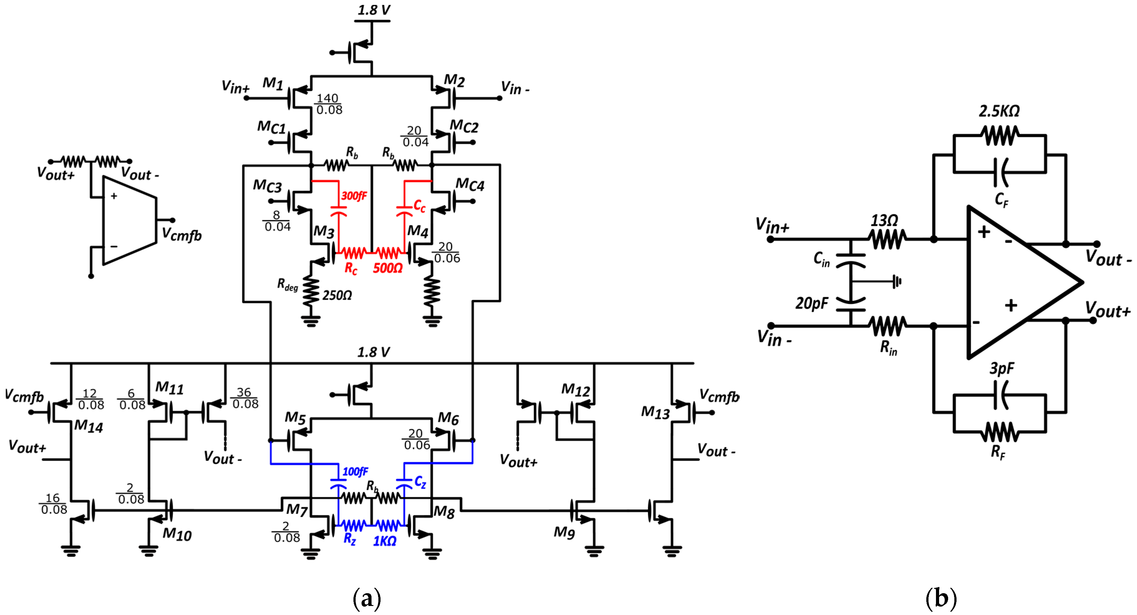
3.1. Low Noise Transconductance Amplifier (LNTA) Design
The LNTA, shown in Figure 5, was designed based on the topology described in detail in [1] and is used in this work primarily because of its low noise and high linearity. High linearity and low noise is achieved using a transformer based complementary common-gate stage with current reuse between NMOS and PMOS input transistors working in class-AB. The three-coil transformer acts as a balun and provides a dual differential signal to the NMOS and PMOS input pairs. The cascode stages provide high output impedance which makes it suitable for proper operation with the current-mode mixer. The main difference with respect to [1] is that the gates of the input transistors are not connected to the primary of the transformer but are simply cross-coupled. A similar approach was also followed in [8]. This allows to eliminate the external balun that was required in [1]. Cross-coupling increases significantly the immunity to common mode signals (including second-order distortion terms) that appear directly at the input of the LNA since they are equally present at the gate and at the source of the input devices. As a result, composed second order nonlinearity, which is the dominant term in the CG LNA third-order distortion, vanishes, boosting the LNA IIP3. This allows to reduce the LNA current from 6 to 4 mA while achieving an IIP3 of around 14 dBm, as shown in Figure 6a.
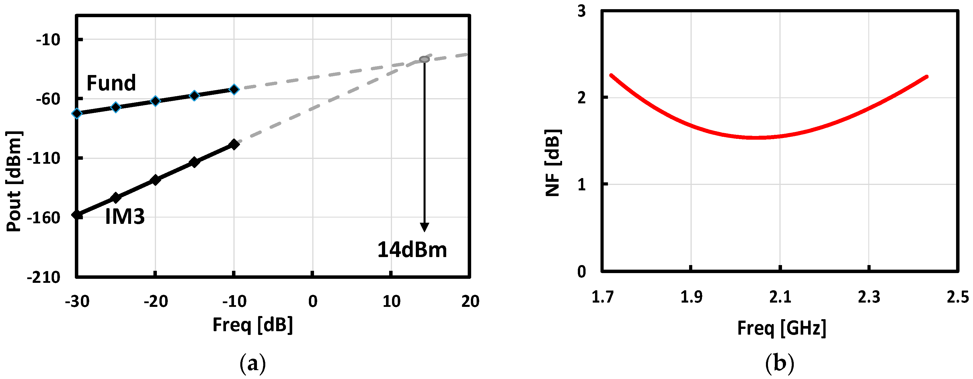
For the same reason, any common-mode second-order distortion term injected by the canceler is also suppressed and does not degrade the receiver IIP3. The noise figure of the LNTA is also improved thanks to cross-coupling. Neglecting transformer losses, the noise factor of the cross-coupled common gate is [29]. Shown in Figure 6b is the simulated NF of the LNA, including transformer losses. It has a NF of 1.6–2.3 dB in the range between 1.7 and 2.4 GHz.
3.2. Active Self-Interference Canceler
The schematic of the proposed active SIC is shown in Figure 5. It consists of two parallel transconductance amplifiers (AMPI and AMPQ) with independently programmable gains and quadrature output phases. To achieve the 360° phase coverage, a replica of the AMPI and AMPQ with inverted polarities is used, but only one of the two instances is active at any given time. Each transconductance amplifier consists of an array of identical elements (slices) that can be independently enabled and disabled, providing a total transconductance gain of 20 ms, digitally programmable with 5-bits of resolution. The cancellation current produced by these amplifiers is injected directly at the secondary terminals of the LNTA input transformer. The canceler is designed to cancel up to −4 dBm of SI signal at the LNTA input and consumes a maximum of 6 mA. Each slice consists of a degenerated complementary transconductance stage. Resistive and capacitive degeneration allow to generate nearly quadrature signals.
In reality, the gate drain-capacitance determines a dominant right-hand side zero in the gain of AMPI (GmI) while the finite transistors transconductance determines a dominant pole in the gain of AMPQ (GmQ), causing a large phase deviation from ideal quadrature. The expressions of GmI and GmQ are
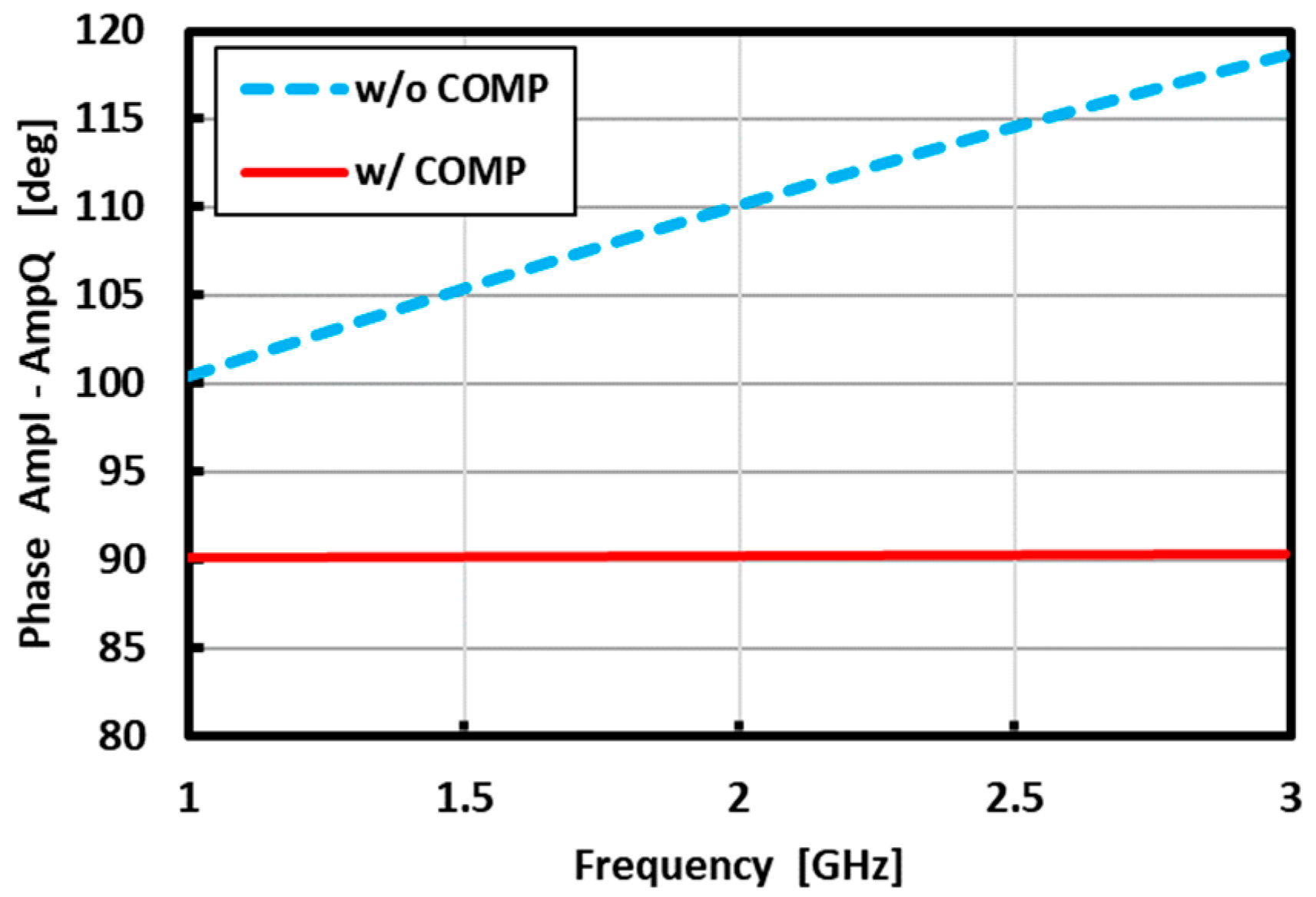
where and at the frequency of interest. is typically at a much higher frequency compared with . As a result, a significant phase error results that creates a tilt in the canceler output vector constellation and reduces the covered range. Adding an explicit capacitance in parallel to the intrinsic gate-drain capacitance of AMPI lowers , eventually canceling out the quadrature phase error (phase compensation). The phase difference between AMPI and AMPQ before and after phase compensation is plotted in Figure 7.
Figure 8 shows the simulated normalized vector gain of the active canceler for all combinations of the control bits before and after the phase error compensation.
3.2.1. Canceler Noise Analysis
The canceler output noise is added directly at the input of the receiver and must be kept low to achieve low overall NF. Both AMPI and AMPQ add noise proportionally based on their transconductance, with AMPQ contributing relatively less noise thanks to the capacitive (noiseless) degeneration. The SI signal at the receiver input determines the cancelling condition set by the magnitude (Gm) and phase () of the canceler transconductance (i.e., the gain settings of AMPI and AMPQ). The noise current injected at the input of the LNTA from the canceller, neglecting the feedback resistors, is given as follows:
where (σ ≈ 1 for γ close to 1). The noise factor expression can be simplified further as a function of the magnitude (Gm) and phase () in relation to the self-interference signal as expressed in (10).
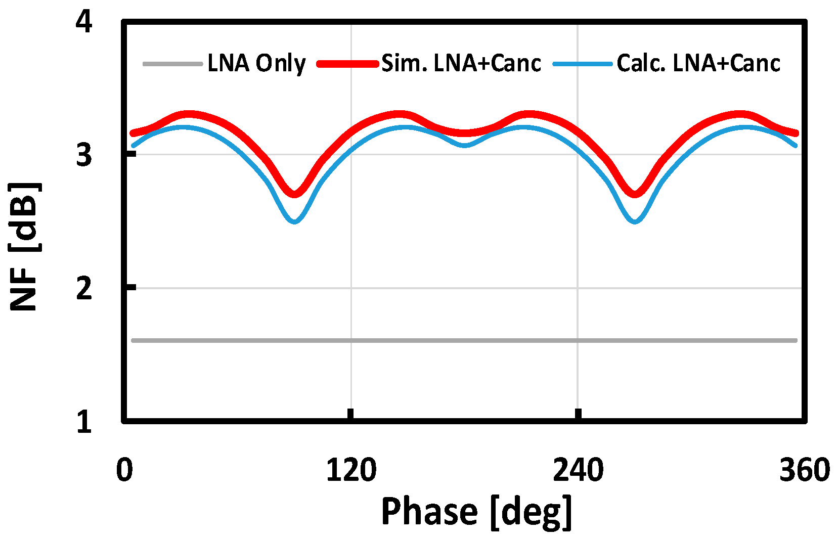
where = is the excess noise factor accounting for the different contributions from AMPI and AMPQ. When AMPQ is OFF and. when AMPI is off, where . The canceler noise factor referred to its input is thus calculated as . The noise current of the canceler referred to the input of the receiver is expressed by: , where n is the LNA input transformer turn ratio, is the differential LNA input impedance and , are the cross coupled feedback resistances for AMPI and AMPQ respectively. For , the canceler and , the maximum noise contribution to the system when AMPI is fully ON, for is a factor of 0.58. The entire noise factor of the system is therefore calculated as , where G is the canceler gain.
Figure 9 shows the simulated and calculated noise figure of the Canceler and LNA only where the calculated noise is expressed as: where = 1.44 at 2 GHz from Figure 6b in Section 3.1.
3.2.2. Canceler Linearization
Due to the finite output conductance of the canceler transistors (MN1-4 and MP1-4), the blocker signal at the canceler output generates cross-modulation products with the TX signal, limiting the effective receiver IIP3. To address this issue, a feedback linearization technique is introduced, as anticipated in section II. The feedback resistors (RFI and RFQ in Figure 5) were sized in such a way that a small fraction of the blocker signal appears at the AMPI and AMPQ inputs, generating intermodulation products that cancel out with the input-output cross modulation terms, improving the receiver effective IIP3. Simulation results will be reported in the next section.
3.3. Baseband Trans-Impedance Amplifier (TIA)
After the LNA a current mode passive mixer driven by a 25% duty-cycle LO was used, followed by a baseband TIA, as shown in Figure 5. The TIA introduces a pole at 22 MHz to attenuate large OOB interferers. The TIA is based on a three-stage operational transconductance amplifier (OTA). The OTA design is based on a similar concept as the one in [30] but it has a wider bandwidth and is designed in 40 nm (versus 28 nm in [30]), which makes the design more challenging. In order to achieve wide bandwidth for better linearity instead of using Miller compensation capacitors, stability is ensured by introducing zeros both within the OTA and in the feedback network. The first stage of the TIA consists of PMOS telescopic—cascode amplifier designed to have high gain in order to ensure high linearity, while the second stage is a full differential pair designed with both moderate gain and distortion, and the third stage work is a complementary class AB, to ensure very high output voltage swing.
Analysing the stability of the TIA, the following critical poles and zeros are identified. The first stage has a dominant pole, ωp,OTA,1 at 32 MHz and a high frequency zero, ωz,OTA,1 = 1/(RcCc). There is also a second pole at high frequency, ωp,OTA,2 ≈ Gm,L/CL,1 that must be well above the unity-gain loop bandwidth. To extend the bandwidth of the second stage, a feed-forward path is introduced through Rz and Cz. This introduces a zero-pole doublet, in which the pole, ωp,OTA,3 at 1/(RzCz) is placed two times the zero frequency, and the zero is used to cancel out the pole introduced by the second stage finite output resistance, ro,2 and its load capacitance, CL,2. Simultaneously, the pole of the second stage, ωp,OTA,3 is compensated for by the zero of the first stage ωz,OTA,1. A second dominant pole at 5 MHz, ωp,OTA,5 is created through the feedback network and the third stage at 1/(Rd//(RF + ro)Cin), where RF is the feedback resistor, Rd is the driving resistance seen looking to the mixer and ro is third stage finite output resistance. In fact, a large Cin (20 pF in this design) helps to filter out the blockers at high frequencies. With two dominant poles, the loop would not be stable. Rin is a small valued resistance placed in series with Cin to introduce a high frequency zero, ωz,OTA,3 at 1/RinCin (around 700 MHz), which is placed before the GBW (at 1.5 GHz) to ensure stability. From the loop gain simulations shown in Figure 11, the loop has a DC gain of around 70 dB, 1.5 GHz GBW and a phase margin of 85°. To ensure a stable DC quiescent point, a common-mode feedback circuit is introduced, and its output is connected to the PMOS of the last stage OTA, as shown in Figure 10.
4. Simulation Results
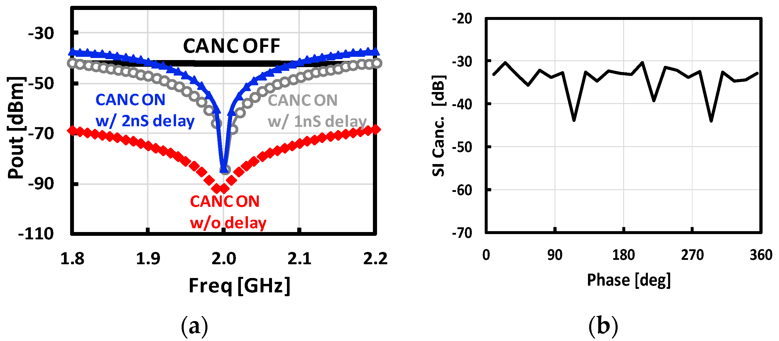
The SIC receiver was designed in 40 nm CMOS technology and has a 1.8 V voltage supply. The active canceler draws a maximum current of 3 mA (AMPI only) or 6 mA (AMPQ only) depending on the self-interference power level and its phase. The LNTA draws a current of 4 mA, while the TIAs draw 1.8 mA each. The total power dissipation is 25 mW. The simulated performance of the canceler alongside the entire receiver chain is reported as follows. Figure 12a shows cancellation of the SI versus frequency when the SI is programmed for optimum cancellation at 2 GHz. 30 dB of cancellation over a bandwidth of 250 MHz is achieved when no delay is introduced between the TX signal and the SI. The 30 dB cancellation bandwidth shrinks to 10 MHz with a delay of 2 ns. Figure 12b also shows the cancellation of the SI as a function of the coupling phase over the entire 360°.
The simulated receiver NF is plotted in Figure 13. When the receiver NF is 4 dB, the noise contribution of the canceler is around 16%, the LNA contributes around 42% and the remaining blocks (Mixer and TIAs) 2%, as illustrated in Figure 13c. The system NF with the canceler turned off is shown in Figure 13a. The system NF without canceler has a NF of 3–3.7 dB in the range of 1.7 and 2.4 GHz. When the canceler is turned ON, it goes from 3.9 dB to 4.5 dB as a function of the coupling phase. The pattern of the noise shown in Figure 13b is consistent with the analysis in Section 3. When AMPI, with degenerated resistor, is turned ON more noise is generated, while when only AMPQ is turned ON the noise decreases.
Figure 14 shows the result of a two-tone test, with one from the TX and one from the blocker at 100 MHz offset. The signal spectrum is shown in Figure 14a. Plotted in Figure 14b is the ratio between blocker and IM3 (HD3) as well as the TX leakage attenuation as a function of canceler gain setting for −6 dBm TX leakage at the receiver input. For the canceler without feedback resistors the peak in HD3 does not correspond to where optimum cancellation is achieved. At the point of optimum SI cancellation, the HD3 is dominated by canceler nonlinearities which is a product of the cross-modulation between the TX signal at the canceler input and the blocker at the LNA input. Adding the feedback resistors re-aligns the peak in HD3 with the peak in SI cancellation.
Figure 15a shows the receiver IIP3 vs the self-interference frequency for both in-band and OOB signals while the canceler is disabled. The two tones (TX leakage) and (blocker) are swept over a range of frequencies such that the intermodulation term is constantly observed at equal to 1 MHz and the LO is at 2 GHz. When the canceler is disabled (dashed line) the receiver IIP3 ranges from 4 dBm in-band to 18 dBm when and are placed 100 MHz and 199 MHz respectively away from the LO. The in-band IIP3 is limited by the TIA. When the canceler is enabled the receiver IIP3 ranges from 36.3 dBm in-band to 34.8 dBm OOB.
The effective IIP3 improvement is strictly related to the cancellation. Ideally, for every 1 dB of SI cancellation, the effective IIP3 should improve by 1 dB, i.e., the IM3 should decrease with the square of cancellation. In plots in Figure 15a, the SI cancellation changes with frequency from 32 dB in-band to 28 dB OOB. This is slightly more than the minimum cancellation of 27 dB that is guaranteed by the canceler resolution. However, it is noticed that the effective OOB IIP3 improvement is much less than the cancellation. This is due to the canceler nonlinearity, ultimately limiting the effective receiver IIP3. This is shown in Figure 16, where the cancellation is varied by adjusting the canceler control bits. When the cancellation is above 18 dB the effective IIP3 remains constant, limited by the canceler intrinsic nonlinearities.
Additional critical system performance test that demonstrates the system full-duplex functionality is carried out by considering an in-band two-tone test with both tones applied at the canceler input, representing the TX signal. The tones are placed at 6 MHz and 10 MHz offset from the LO and the IM3 falls at 2 MHz. When the canceler is disabled, the IIP3 is equal to 5.3 dBm. When the canceler is turned on and set to the proper setting for SI cancellation, the IIP3 improves to 21 dBm, as is illustrated by the simulation results in Figure 17. One interesting observation is that the result shows that the output IM3 of the canceler becomes dominant at the RX input. In fact, in the SI cancellation full-duplex system, the effective receiver IIP3 is given by the canceler IIP3 plus 3 dB, due to the LNA input transformer gain (−3 dB). The IIP3 of the canceler is thus, important and must be designed to be sufficiently high to guarantee both FDD and full-duplex operations.
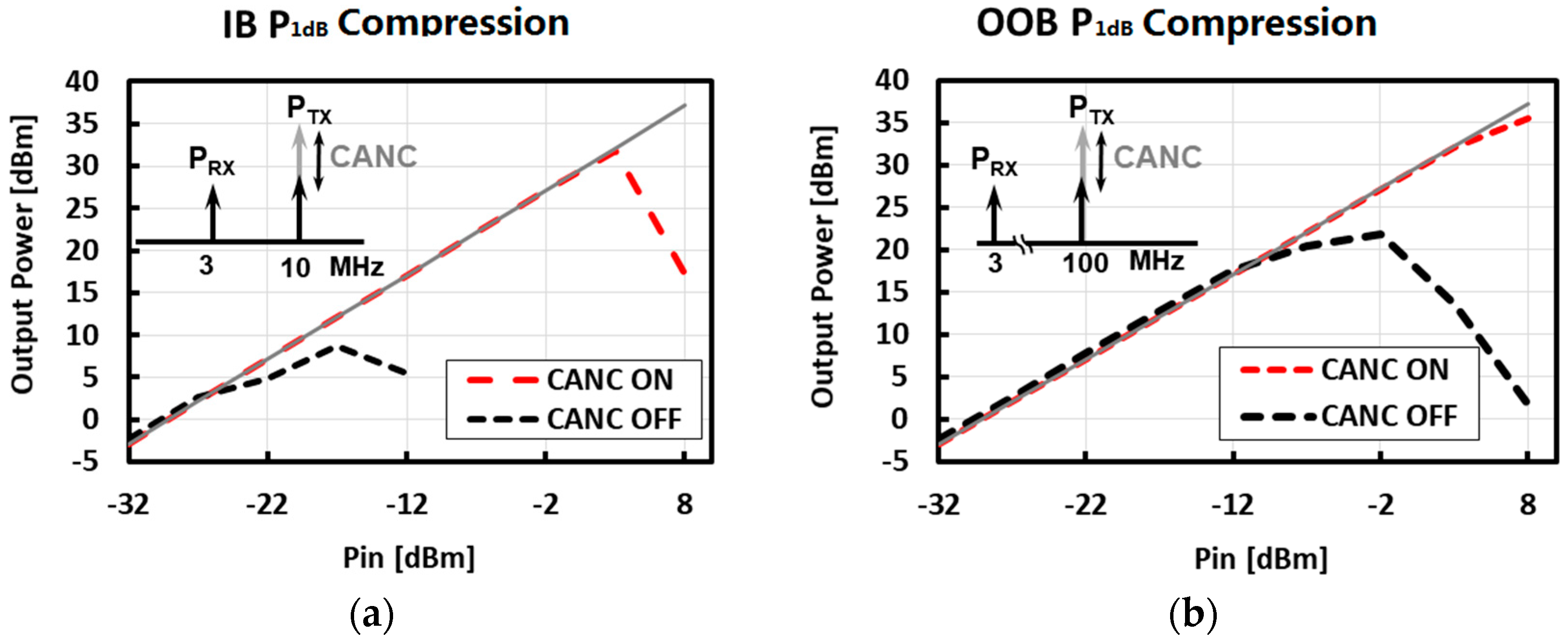
Another performance evaluation of the receiver with the canceler is the 1 dB compression point (P1dB). With the canceler disabled, the receiver, due to the presence of SI saturates, thereby desensitizing the RX signal. The gain 1 dB compression plot due to an in-band SI is shown in Figure 18a. The simulation result is obtained with the SI placed at 10 MHz away from the LO (at 2 GHz) while the Rx signal is placed at 3 MHz offset. The in-band P1dB referred to the receiver input is −25 dBm. When the canceler is turned ON, with more than 30 dB of SI cancellation, P1dB is pushed to 4 dBm. For the OOB P1dB evaluation, the SI is placed 100 MHz away from the LO and the Rx signal is kept at 3 MHz. The receive signal is swept until saturation occurred at 1.7 dBm referred to the RX port while the canceler is disabled. When the canceler is turned on, the P1dB is pushed to 5 dBm, as plotted in Figure 18b.
This work is benchmarked against prior works focussing on SI cancellation for FDD and full-duplex systems [12,18,20,21] as shown in Table 1. The system achieves low noise figure and high effective IIP3 thanks to the improvement of the canceler cross-modulation distortion, while dissipating low power. TX leakage cancellation is performed in front of the LNA achieving more than 30 dB of cancellation over 80 MHz bandwidth. This solution addresses also the issues of receiver IIP2 and reciprocal mixing. Among prior works, only [18], which is tailored towards FDD applications, achieves similar IIP3 values and higher SI power handling capabilities. However, the TX leakage is effectively cancelled only after down-conversion and recombination between common-gate and common-source paths, making it prone to IIP2 and reciprocal mixing. Furthermore [18] has much higher power dissipation and higher NF. In [12] power dissipation is very low but the maximum SI is only −20 dBm. However, to be fair, it must be noticed that all of the other works reported in the table report measured results, while in this work we are presenting only simulation results.
5. Conclusions
A highly linear and low noise receiver front-end is proposed for dual antenna systems (for Full duplex and FDD) that is based on an active self-interference canceler with a 5-bit resolution to implement an active programmable vector modulator. To meet the FD requirements, the SI cancellation can be improved in the digital domain [10]. The proposed canceler strongly attenuates the TX leakage of up to −4 dBm of power at the input of the LNA, with benefits for the entire receiver in terms of IIP3, IIP2 and reciprocal mixing. A cross-modulation mechanism of the canceler was identified and strongly suppressed thanks to resistive feedback. The effective OOB IIP3 of the receiver was improved from 14 dBm with the canceler disabled to 35 dBm with the canceler enabled. Compared with previous implementations, lower power, lower noise, and higher IIP3 with respect to self-interference was achieved.
Author Contributions
Saheed Tijani is the main author and responsible for writing the paper. Danilo Manstretta was responsible for the review and supervising of the paper.
Conflicts of Interest
The authors declare no conflict of interest.
References
- Fabiano, I.; Sosio, M.; Liscidini, A.; Castello, R. SAW-less analog front-end receivers for TDD and FDD. IEEE J. Solid-State Circuits 2013, 48, 3067–3079. [Google Scholar] [CrossRef]
- Bharadia, D.; McMilin, E.; Katti, S. Full Duplex Radios. In Proceedings of the ACM SIGCOMM, Hong Kong, China, 12–16 August 2013. [Google Scholar]
- Huusari, T.; Choi, Y.S.; Liikkanen, P.; Korpi, D.; Talwar, S.; Valkama, M. Wideband Self-Adaptive RF Cancellation Circuit for Full-Duplex Radio: Operating Principle and Measurements. In Proceedings of the 2015 IEEE 81st Vehicular Technology Conference (VTC Spring), Glasgow, UK, 11–14 May 2015; pp. 1–7. [Google Scholar]
- Tamminen, J.; Turunen, M.; Korpi, D.; Huusari, T.; Choi, Y.; Talwar, S.; Valkama, M. Digitally-controlled RF self-interference canceller for full-duplex radios. In Proceedings of the 2016 24th European Signal Processing Conference (EUSIPCO), Budapest, Hungary, 29 August–2 September 2016; pp. 783–787. [Google Scholar]
- Kiayani, A.; Anttila, L.; Valkama, M. Active RF cancellation of nonlinear TX leakage in FDD transceivers. In Proceedings of the 2016 IEEE Global Conference on Signal and Information Processing (GlobalSIP), Washington, DC, USA, 7–9 December 2016; pp. 689–693. [Google Scholar]
- Roverato, E.; Kosunen, M.; Cornelissens, K.; Vatti, S.; Stynen, P.; Bertrand, K.; Korhonen, T.; Samsom, H.; Vandenameele, P.; Ryynänen, J.; et al. 13.4 All-digital RF transmitter in 28 nm CMOS with programmable RX-band noise shaping. In Proceedings of the 2017 IEEE International Solid-State Circuits Conference (ISSCC), San Francisco, CA, USA, 5–6 February 2017; pp. 222–223. [Google Scholar]
- Abdelhalem, S.H.; Gudem, P.S.; Larson, L.E. Hybrid Transformer-Based Tunable Differential Duplexer in a 90-nm CMOS Process. IEEE Trans. Microw. Theory Tech. 2013, 61, 1316–1326. [Google Scholar] [CrossRef]
- Fabiano, I.; Ramella, M.; Manstretta, D.; Castello, R. A +25 dBm IIP3 1.7–2.1 GHz FDD Receiver Front-End with Integrated Hybrid-Transformer in 28 nm CMOS. IEEE Trans. Microw. Theory Tech. 2017, 65, 4677–4688. [Google Scholar] [CrossRef]
- Calderin, L.; Ramakrishnan, S.; Puglielli, A.; Alon, E.; Nikolić, B.; Niknejad, A.M. Analysis and Design of Integrated Active Cancellation Transceiver for Frequency Division Duplex Systems. IEEE J. Solid-State Circuits 2017, 52, 2038–2054. [Google Scholar] [CrossRef]
- Zhou, J.; Reiskarimian, N.; Krishnaswamy, H. 9.8 Receiver with integrated magnetic-free N-path-filter-based non-reciprocal circulator and baseband self-interference cancellation for full-duplex wireless. In Proceedings of the 2016 IEEE International Solid-State Circuits Conference (ISSCC), San Francisco, CA, USA, 31 January–4 February 2016; pp. 178–180. [Google Scholar]
- Zhang, T.; Suvarna, A.R.; Bhagavatula, V.; Rudell, J.C. An Integrated CMOS Passive Self-Interference Mitigation Technique for FDD Radios. IEEE JSSC 2015, 50, 1176–1188. [Google Scholar] [CrossRef]
- Zhang, T.; Chen, Y.; Huang, C.; Rudell, J.C. A Low-Noise Reconfigurable Full-Duplex Front-End with Self-Interference Cancellation and Harmonic-Rejection Power Amplifier for Low Power Radio Applications. In Proceedings of the 43rd European Solid-State Circuit Conference (ESSCIRC), Leuven, Belgium, 11–14 September 2017. [Google Scholar]
- Reiskarimian, N.; Dastjerdi, M.B.; Zhou, J.; Krishnaswamy, H. Highly-linear integrated magnetic-free circulator-receiver for full-duplex wireless. In Proceedings of the 2017 IEEE International Solid-State Circuits Conference (ISSCC), San Francisco, CA, USA, 5–9 February 2017; pp. 316–317. [Google Scholar]
- Yang, D.; Yuksel, H.; Molnar, A. A Wideband Highly Integrated and Widely Tunable Transceiver for In-Band Full-Duplex Communication. IEEE J. Solid-State Circuits 2015, 50, 1189–1202. [Google Scholar] [CrossRef]
- Ramakrishnan, S.; Calderin, L.; Niknejad, A.; Nikolić, B. An FD/FDD transceiver with RX band thermal, quantization, and phase noise rejection and 64 dB TX signal cancellation. In Proceedings of the 2017 IEEE Radio Frequency Integrated Circuits Symposium (RFIC), Honolulu, HI, USA, 4–6 June 2017; pp. 352–355. [Google Scholar]
- Ayati, S.A.; Mandal, D.; Bakkaloglu, B.; Kiaei, S. Adaptive integrated CMOS circulator. In Proceedings of the 2016 IEEE Radio Frequency Integrated Circuits Symposium (RFIC), San Francisco, CA, USA, 22–24 May 2016; pp. 146–149. [Google Scholar]
- Zhou, J.; Chakrabarti, A.; Kinget, P.; Krishnaswamy, H. Low-Noise Active Cancellation of Transmitter Leakage and Transmitter Noise in Broadband Wireless Receivers for FDD/Co-Existence. IEEE J. Solid-State Circuits 2014, 49, 3046–3062. [Google Scholar] [CrossRef]
- Luo, C.; Gudem, P.S.; Buckwalter, J.F. 0.4–6 GHz,17-dBm B1dB, 36-dBm IIP3 Channel-selecting, Low-noise Amplifier for SAW-less 3G/4G FDD Receivers. In Proceedings of the IEEE RFIC Symposium, Phoenix, AZ, USA, 17–19 May 2015. [Google Scholar]
- Zhou, J.; Chuang, T.H.; Dinc, T.; Krishnaswamy, H. Reconfigurable Receiver with >20 MHz bandwidth self-interference cancellation suitable for FDD, co-existence and full-duplex applications. In Proceedings of the 2015 IEEE International Solid-State Circuits Conference (ISSCC), San Francisco, CA, USA, 22–26 February 2015; pp. 342–343. [Google Scholar]
- Van den Broek, D.J.; Klumperink, E.A.M.; Nauta, B. A self-interference-cancelling receiver for in-band full-duplex wireless with low distortion under cancellation of strong TX leakage. In Proceedings of the 2015 IEEE ISSCC, San Francisco, CA, USA, 22–26 February 2015. [Google Scholar]
- Zhang, T.; Najafi, A.; Su, C.; Rudell, J.C. 18.1 A 1.7-to-2.2 GHz full-duplex transceiver system with >50 dB self-interference cancellation over 42 MHz bandwidth. In Proceedings of the 2017 IEEE International Solid-State Circuits Conference (ISSCC), San Francisco, CA, USA, 5–6 February 2017; pp. 314–315. [Google Scholar]
- Tijani, S.; Manstretta, D. A SAW-less receiver front-end with low power active self-interference canceler. In Proceedings of the 2015 IEEE International Conference on Electronics, Circuits, and Systems (ICECS), Cairo, Egypt, 6–9 December 2015; pp. 89–92. [Google Scholar]
- Montanari, D.; Silvestri, L.; Bozzi, M.; Manstretta, D. Antenna coupling and self-interference cancellation bandwidth in SAW-less diversity receivers. In Proceedings of the 2016 46th European Microwave Conference (EuMC), London, UK, 4–6 October 2016; pp. 731–734. [Google Scholar]
- Montanari, D.; Castellano, G.; Manstretta, D.; Castello, R. A 0.7–2 GHz Auxiliary Receiver with Enhanced Compression for SAW-less FDD. In Proceedings of the 43rd European Solid-State Circuit Conference (ESSCIRC), Leuven, Belgium, 11–14 September 2017. [Google Scholar]
- Yang, X.; Babakhani, A. A 4.6–5.35 GHz transceiver with 38 dB on-chip self-interference cancelation at 10 kHz offset frequency. In Proceedings of the 2015 IEEE Radio Frequency Integrated Circuits Symposium (RFIC), Phoenix, AZ, USA, 17–19 May 2015; pp. 239–242. [Google Scholar]
- ETSI. LTE (E-UTRA) User Equipment (UE) Radio Transmission and Reception, 3GPP TS 136.101 ver. 12.5.0, Release 12. November 2014. Available online: http://www.etsi.org/deliver/etsi_ts/136100_136199/136101/12.05.00_60/ts_136101v120500p.pdf (accessed on 21 August 2017).
- Kim, H.; Woo, S.; Jung, S.; Lee, K.-L. A CMOS Transmitter Leakage Canceller for WCDMA Applications. IEEE Trans. Microw. Theory Tech. 2013, 61, 3373–3380. [Google Scholar] [CrossRef]
- Van den Broek, D.J.; Klumperink, E.A.M.; Nauta, B. An In-Band Full-Duplex Radio Receiver with a Passive Vector Modulator Downmixer for Self-Interference Cancellation. IEEE J. Solid-State Circuits 2015, 50, 3003–3014. [Google Scholar] [CrossRef]
- Zhuo, W.; Embabi, S.; de Gyvez, J.P.; Sanchez-Sinencio, E. Using capacitive cross-coupling technique in RF low noise amplifiers and down-conversion mixer design. In Proceedings of the 26th European Solid-State Circuits Conference, Stockholm, Sweden, 19–21 September 2000; pp. 77–80. [Google Scholar]
- Pini, G.; Manstretta, D.; Castello, R. Highly linear TIA for SAW-less FDD receivers. In Proceedings of the 2016 IEEE Asian Solid-State Circuits Conference (A-SSCC), Toyama, Japan, 7–9 November 2016; pp. 117–120. [Google Scholar]
Figure 1.
System block diagram.
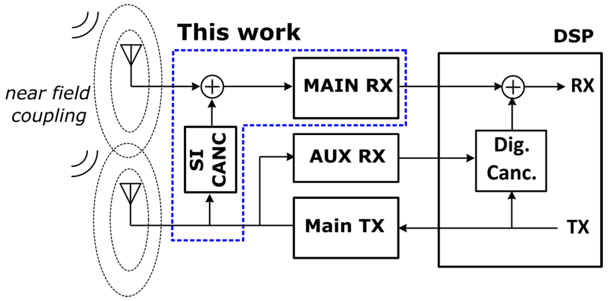
Figure 2.
Canceler feedback linearization.
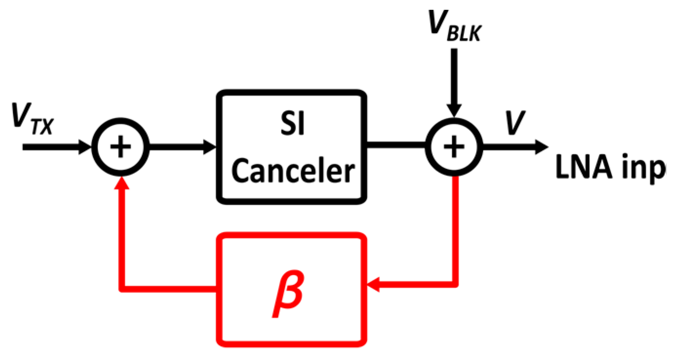
Figure 3.
(a) Canceler block design concept; (b) Canceler gain adjustment.

Figure 4.
(a) Quadrature phase error; (b) Canceler range reduction due to quadrature phase error; (c) Cancellation in dB with corresponding output vector magnitude and phase error.
Figure 4.
(a) Quadrature phase error; (b) Canceler range reduction due to quadrature phase error; (c) Cancellation in dB with corresponding output vector magnitude and phase error.
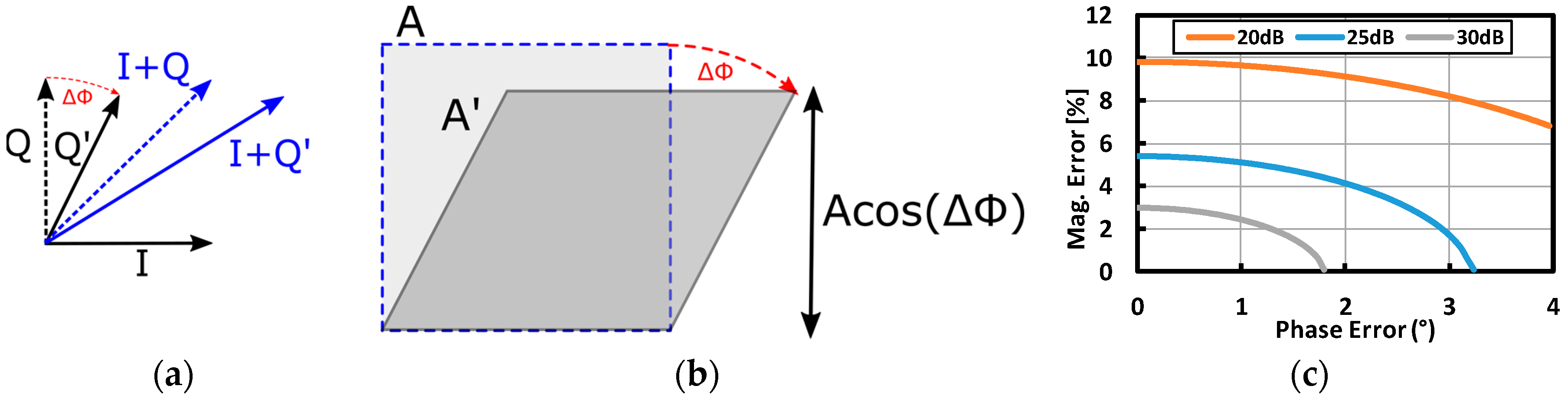
Figure 5.
System architecture: Active self-interference (SI) canceler, Low Noise Transconductance Amplifier (LNTA), passive mixer, and transimpedance filter.
Figure 5.
System architecture: Active self-interference (SI) canceler, Low Noise Transconductance Amplifier (LNTA), passive mixer, and transimpedance filter.
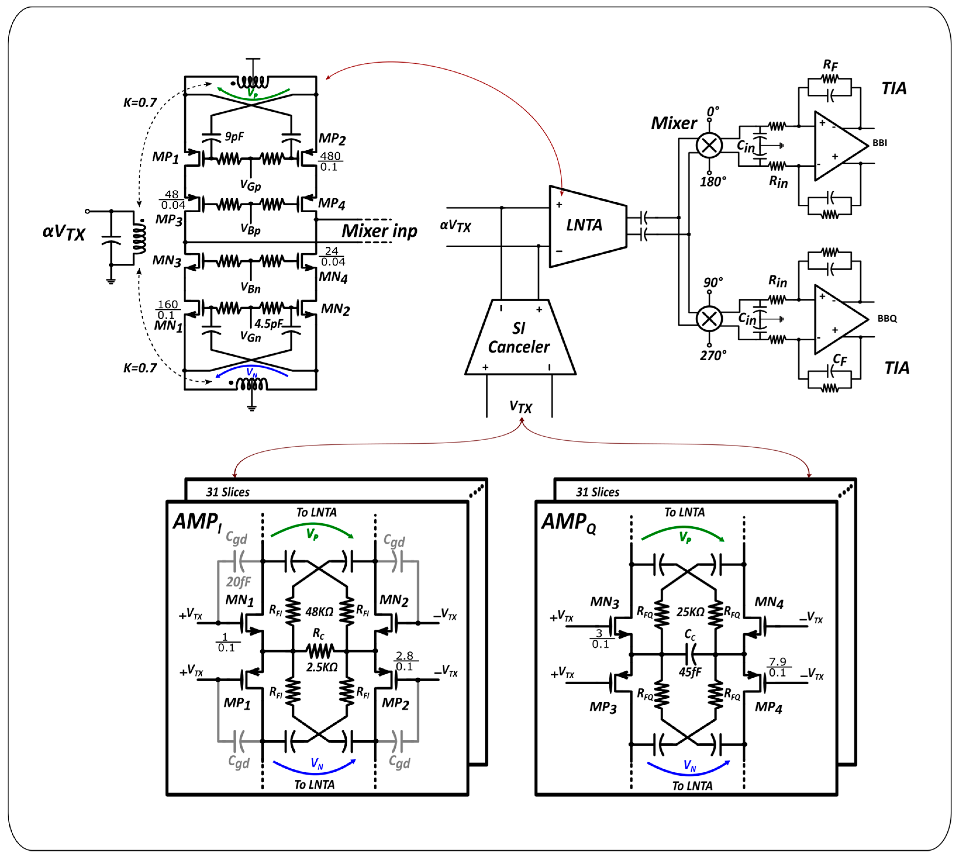
Figure 6.
(a) LNA IIP3; (b) LNA NF vs. RF frequency.

Figure 7.
Quadrature error compensation.

Figure 8.
Canceler constellation: (a) before compensation; (b) after compensation.
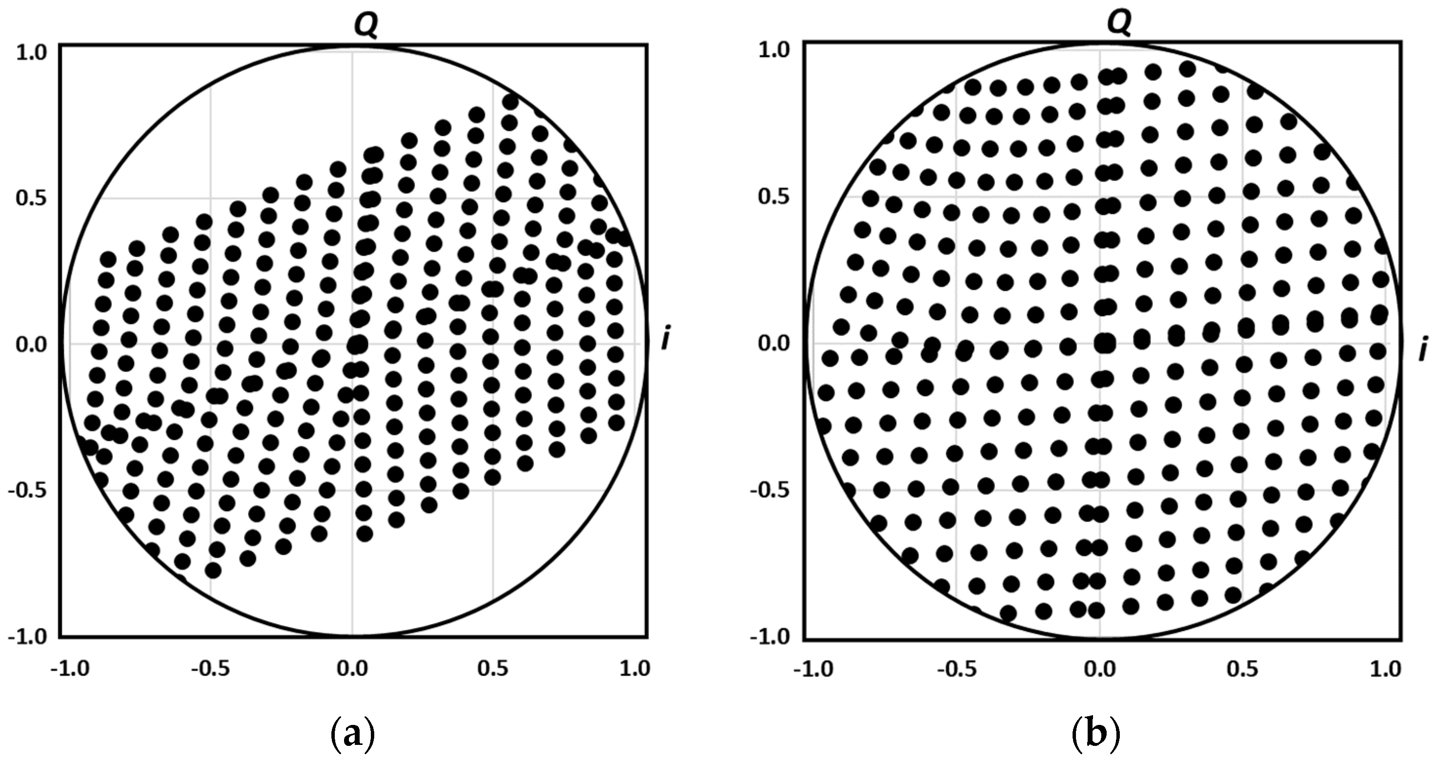
Figure 9.
Noise figure of LNA with canceler as function of the phase shift.

Figure 10.
(a) Schematic of the three-stage operational transconductance amplifier (OTA); (b) TIA schematic.
Figure 10.
(a) Schematic of the three-stage operational transconductance amplifier (OTA); (b) TIA schematic.

Figure 11.
Loop gain magnitude and phase of the trans-impedance amplifiers (TIA).
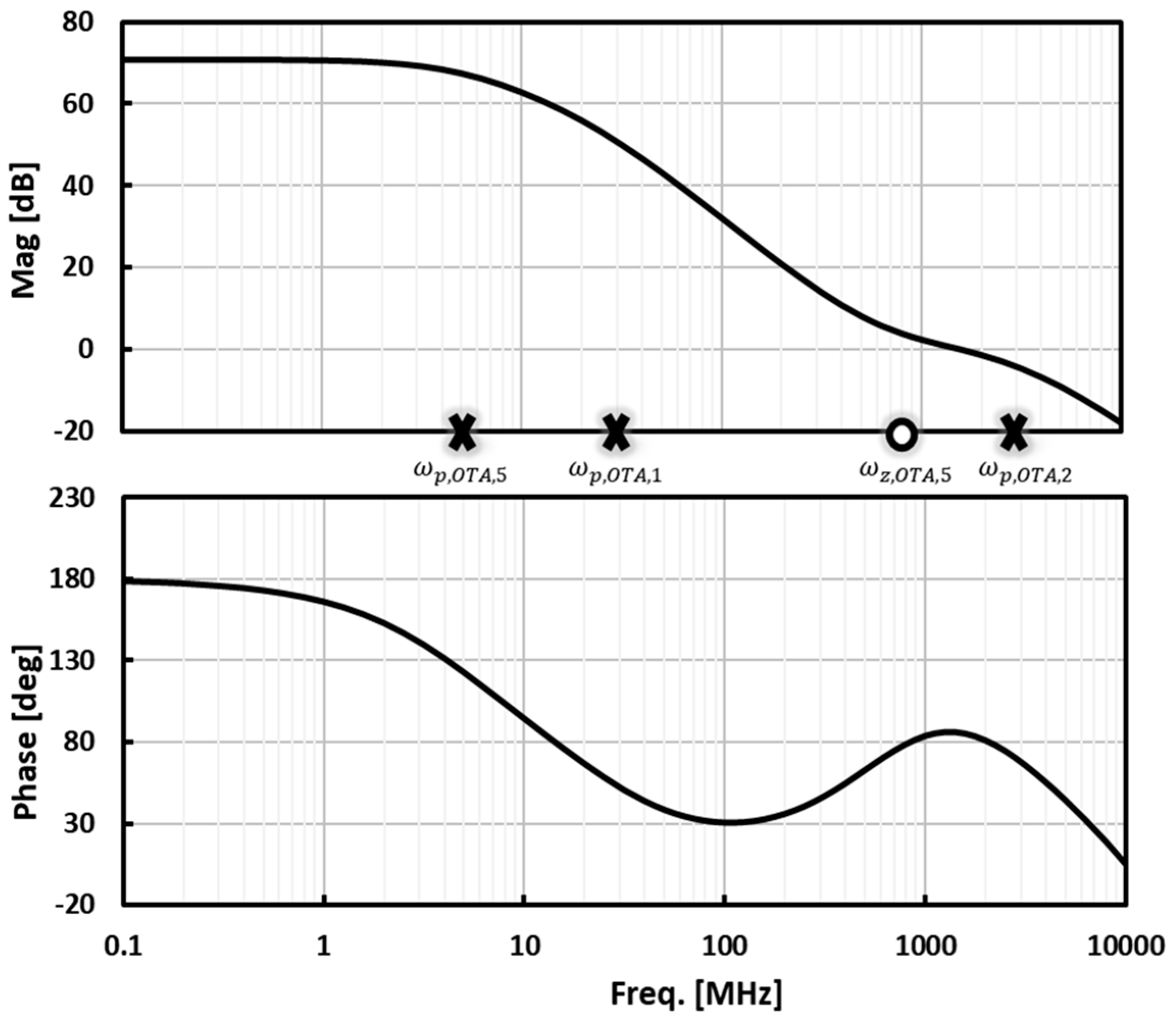
Figure 12.
Self-interference cancellation (a) over RF frequency; (b) as a function of canceler phase.
Figure 12.
Self-interference cancellation (a) over RF frequency; (b) as a function of canceler phase.

Figure 13.
RX NF (a) vs. input frequency; (b) with and without canceler as a function of canceler phase; (c) Noise summary of the system.
Figure 13.
RX NF (a) vs. input frequency; (b) with and without canceler as a function of canceler phase; (c) Noise summary of the system.
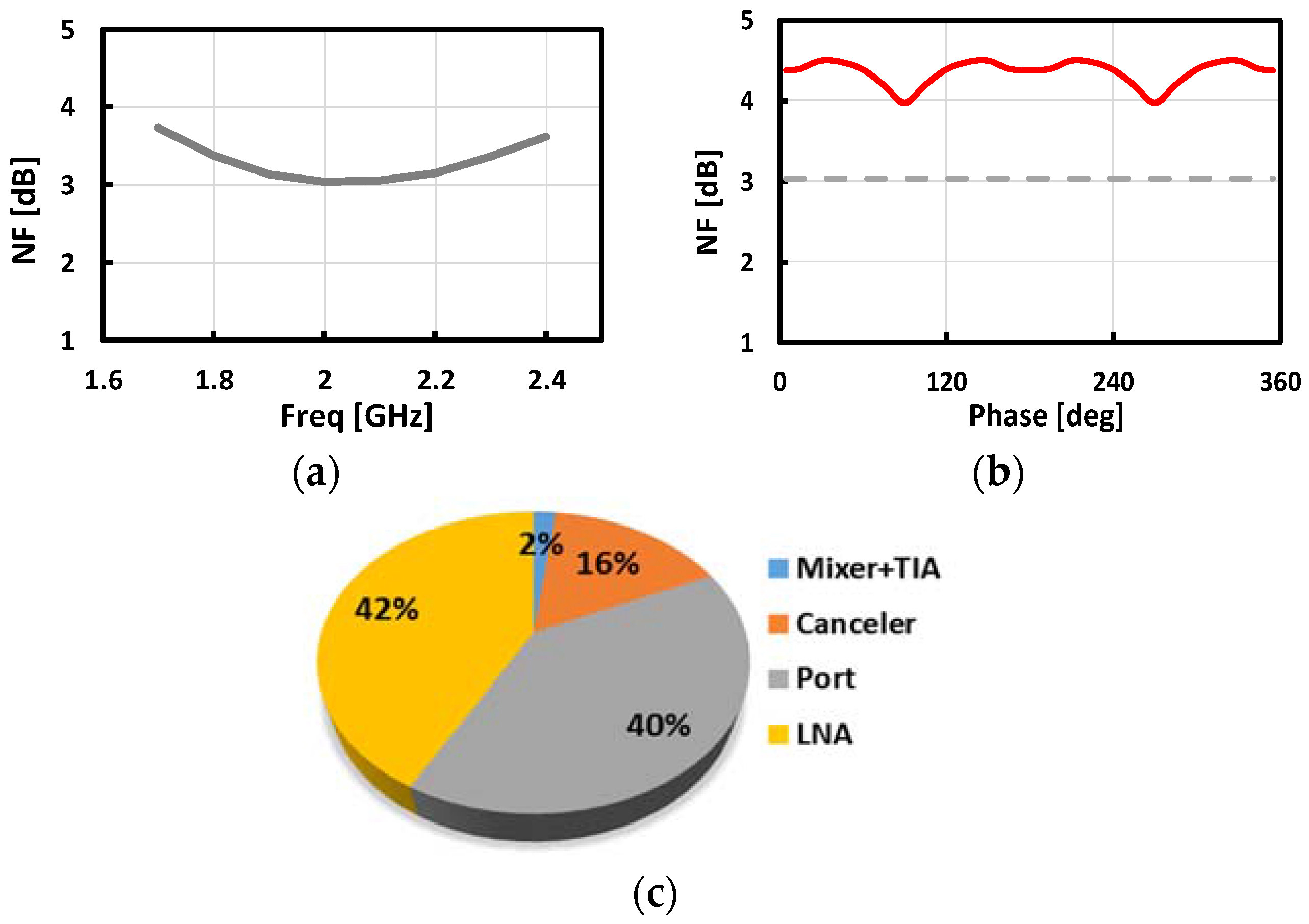
Figure 14.
Two-tone test: (a) spectrum with blocker at 10 MHz offset; (b) with SI at the RX input as a function of canceler control bits.
Figure 14.
Two-tone test: (a) spectrum with blocker at 10 MHz offset; (b) with SI at the RX input as a function of canceler control bits.

Figure 15.
Receiver gain and effective IIP3 before and after cancellation: (a) vs. two-tone frequency spacing; (b) vs. input power for a frequency spacing of 45 MHz.
Figure 15.
Receiver gain and effective IIP3 before and after cancellation: (a) vs. two-tone frequency spacing; (b) vs. input power for a frequency spacing of 45 MHz.
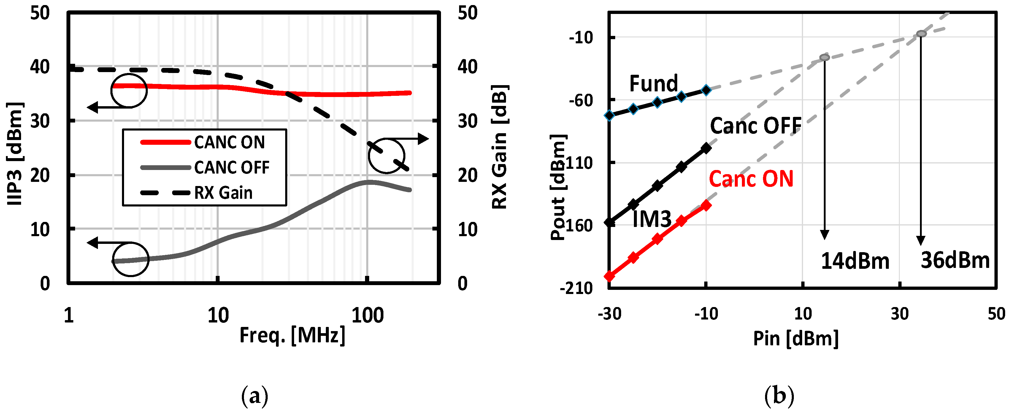
Figure 16.
Effective OOB IIP3 vs. SI cancellation.
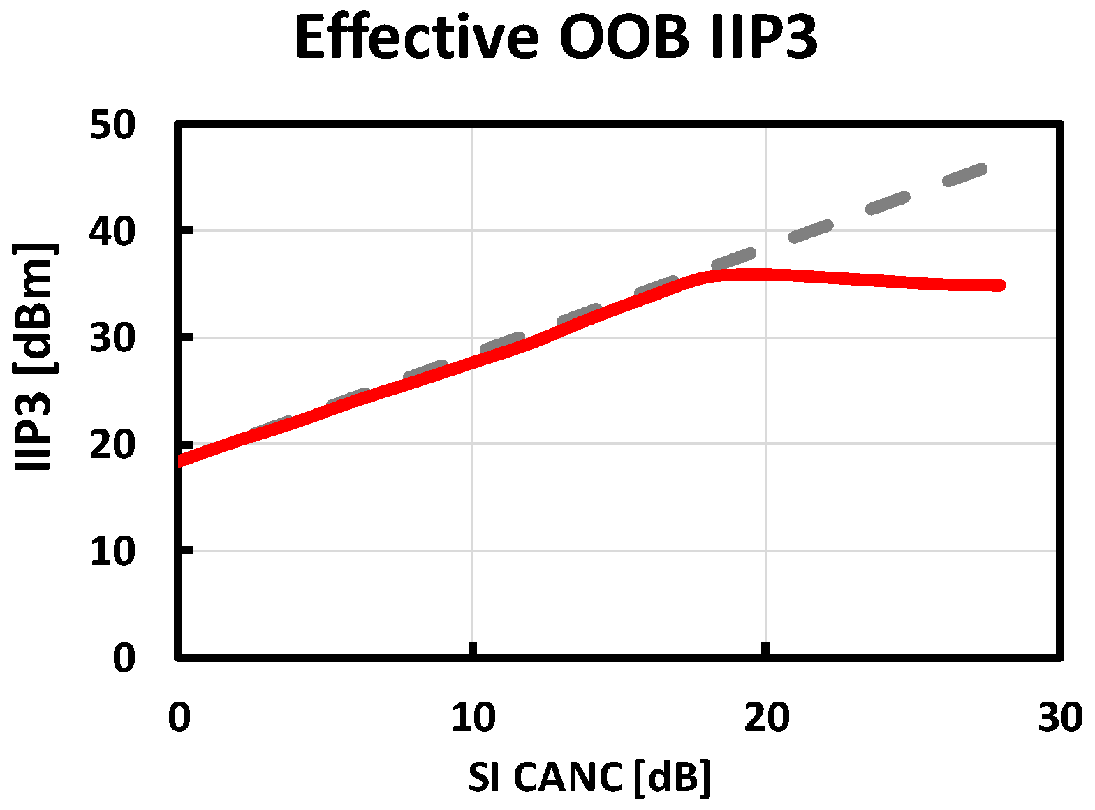
Figure 17.
IIP3 with two-tone cancellation at receiver (RX) input.
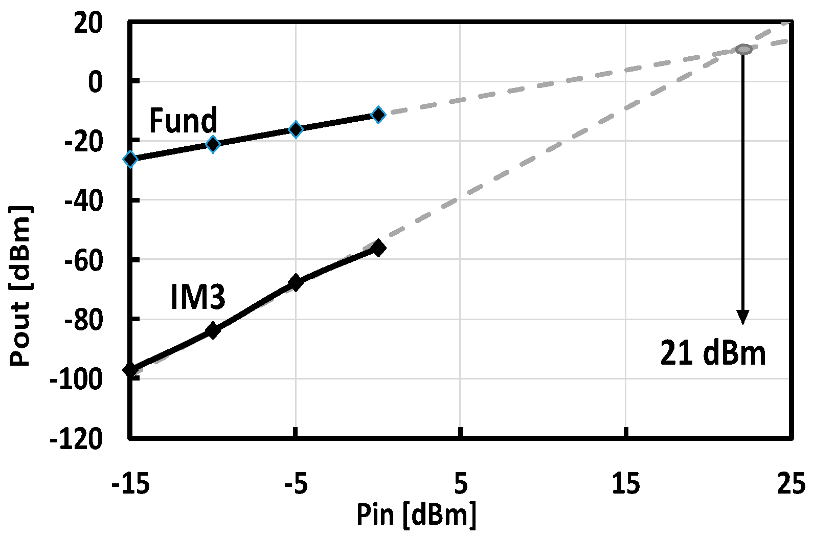
Figure 18.
Receiver P1dB compression with and without the canceler: (a) In-band compression at 11 MHz; (b) Out of band compression at 100 MHz as function of input power.
Figure 18.
Receiver P1dB compression with and without the canceler: (a) In-band compression at 11 MHz; (b) Out of band compression at 100 MHz as function of input power.


Table 1.
Performance comparison.
| This Work | [18] b JSSC ’14 | [20] b ISSCC ’15 | [21] b ISSCC ’15 | [12] b ESSCIRC ’15 | |
|---|---|---|---|---|---|
| FDD/FD | FD/FDD | FDD | FDD/FD | FD | FD |
| Technology | 40 nm | 65 nm | 65 nm | 65 nm | 40 nm |
| CMOS | CMOS | CMOS | CMOS | CMOS | |
| Frequency | 1.5–2.5 GHz | 0.5–1.5 GHz | 0.8–1.4 GHz | 0.15–3.5 GHz | 1–3 GHz |
| NF w/o canc | 3 dB | 4.2–5.6 dB | 4.8–5.8 dB | 6.3 dB | 4.8–5.8 dB |
| NF w/canc | 3.9–4.6 dB | 5–6.4 dB | 5.3/7 dB | 10.3–12.3 dB | 5.3/7 dB |
| IP3 RX | 14 dBm | 12 dBm | 17/−22 dBm | 16.2 dBm a | 18 dBm |
| Eff. IIP3 | 35 dBm | 33 dBm | 27/2 dBm | 19 dBm a | N/A |
| SI Cancellation | >30 dB | 30 dB | 20 dB | 27 dB | 30 dB |
| /250 c–10 d MHz | /25 MHz | /4 MHz | |||
| Max TX Leak. | −4 dBm | +2 dBm | −8 dBm | 1.5 dBm | −20 dBm |
| Power | 14 mW RX | 83 mW RX 72 | 69 mW RX | 23–56 mW | 11 mW RX |
| 11 mW canc | mW canc | 91 mW/path | 0.6 mW/Cac |
a In-band IIP3; b measured results; c without delay between transmitter (TX)/RX; d with 2 ns group delay.
© 2017 by the authors. Licensee MDPI, Basel, Switzerland. This article is an open access article distributed under the terms and conditions of the Creative Commons Attribution (CC BY) license (http://creativecommons.org/licenses/by/4.0/).
Share and Cite
MDPI and ACS Style
Tijani, S.; Manstretta, D. A Low-Power Active Self-Interference Cancellation Technique for SAW-Less FDD and Full-Duplex Receivers. J. Low Power Electron. Appl. 2017, 7, 27. https://doi.org/10.3390/jlpea7040027
AMA Style
Tijani S, Manstretta D. A Low-Power Active Self-Interference Cancellation Technique for SAW-Less FDD and Full-Duplex Receivers. Journal of Low Power Electronics and Applications. 2017; 7(4):27. https://doi.org/10.3390/jlpea7040027
Chicago/Turabian StyleTijani, Saheed, and Danilo Manstretta. 2017. "A Low-Power Active Self-Interference Cancellation Technique for SAW-Less FDD and Full-Duplex Receivers" Journal of Low Power Electronics and Applications 7, no. 4: 27. https://doi.org/10.3390/jlpea7040027
Note that from the first issue of 2016, this journal uses article numbers instead of page numbers. See further details here.