Physical, Electrical, and Reliability Considerations for Copper BEOL Layout Design Rules

Abstract
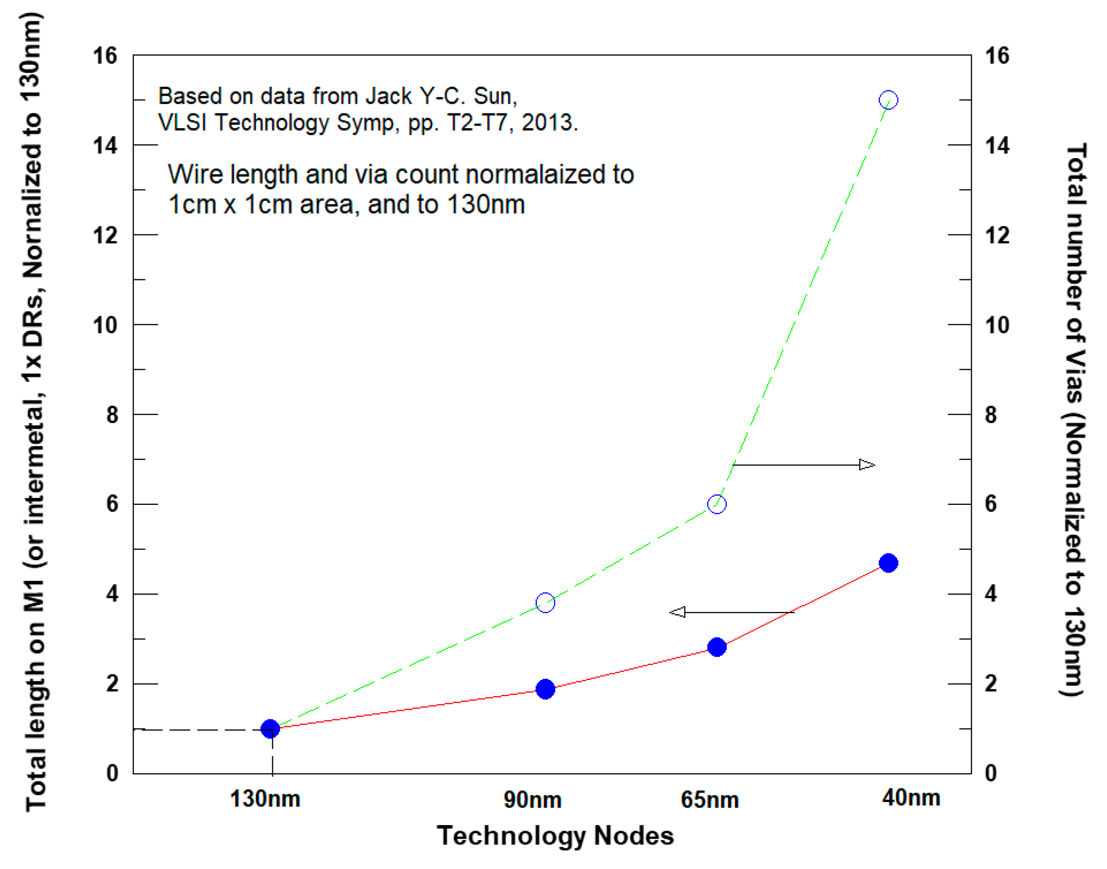
1. Introduction
2. Methodology for BEOL Design Rule Setting
- (i)
- Technology process performance in terms of nominal process targets (like critical dimensions), as well as the accuracy requirement. Basically, the DR “limit” should reflect the “worst-case” process conditions. In practice, a large amount of process data should be collected and analyzed, including aspects of in–die wafer variation, die–to–die (D2D), wafer–to–wafer (W2W), and lot–to–lot (L2L) differences. In addition, to enhance manufacturing cycle-time, the production floor uses several process tools for each step. This is another important aspect that introduces variability.
- (ii)
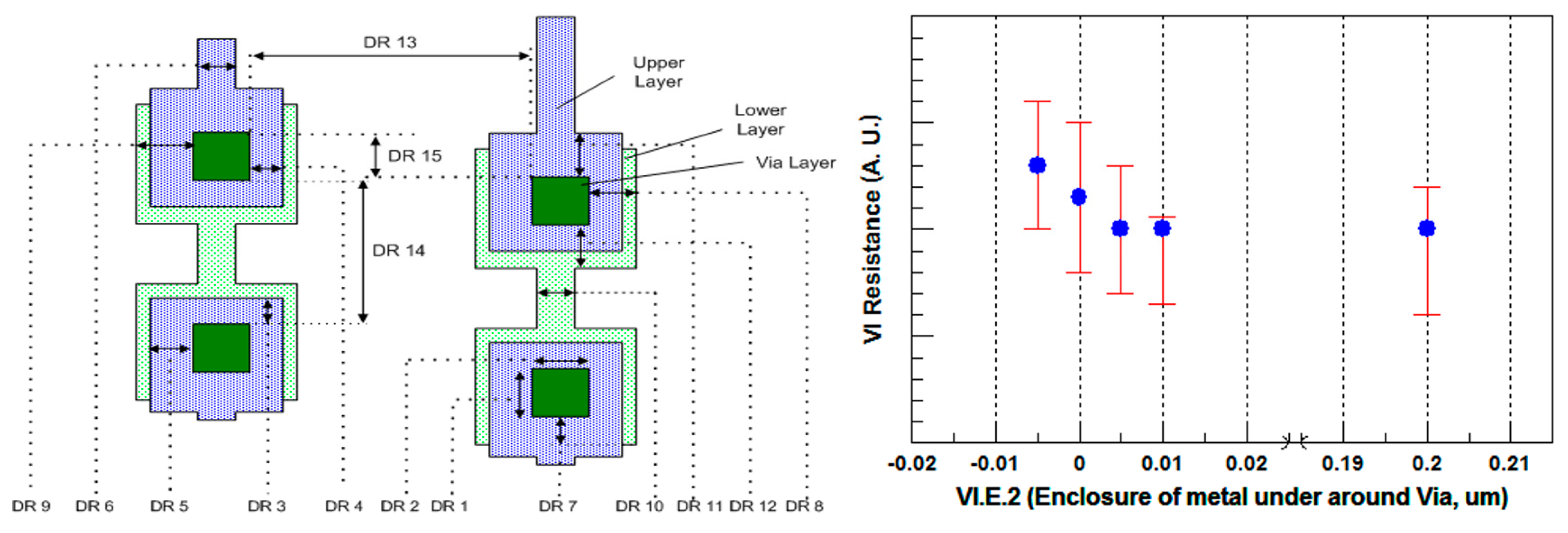
- Sensitivity of the relevant electrical parameter to the process variation. For example, the dependence of the first metal “open” (un-connected M1 line) to M1 nominal width and variability. Some of the dependencies are very clear. However, some require integration of certain aspects of interaction between several layers. For example, the overall sensitivity of the via resistance depends not only on the via size (that is fixed in the design), but also on the enclosure of the metals below and above the via. A small via or insufficient metal enclosure below or above will result in higher via resistance. Therefore, in order to maintain stable via resistance, several rules should be defined.
- (iii)
- Sensitivity of the reliability parameter relevant to the process. For example, the effect of a very narrow M1 line on the maximum current allowed the elimination of working at the EM conditions.
- (iv)
- Scaling demands and manufacturing costs.
3. Contact Related Rules
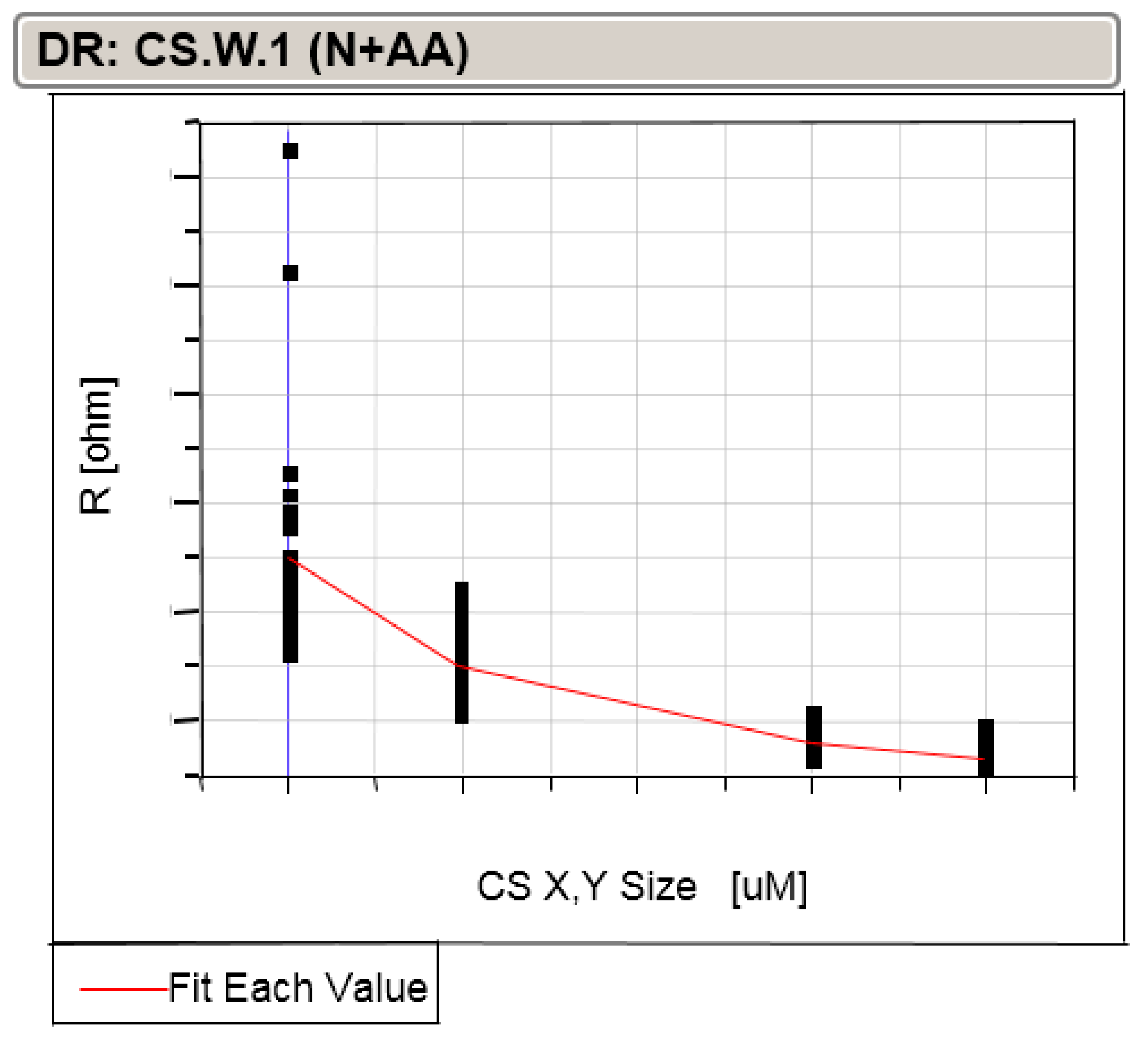
3.1. Contact Width and Space Rules
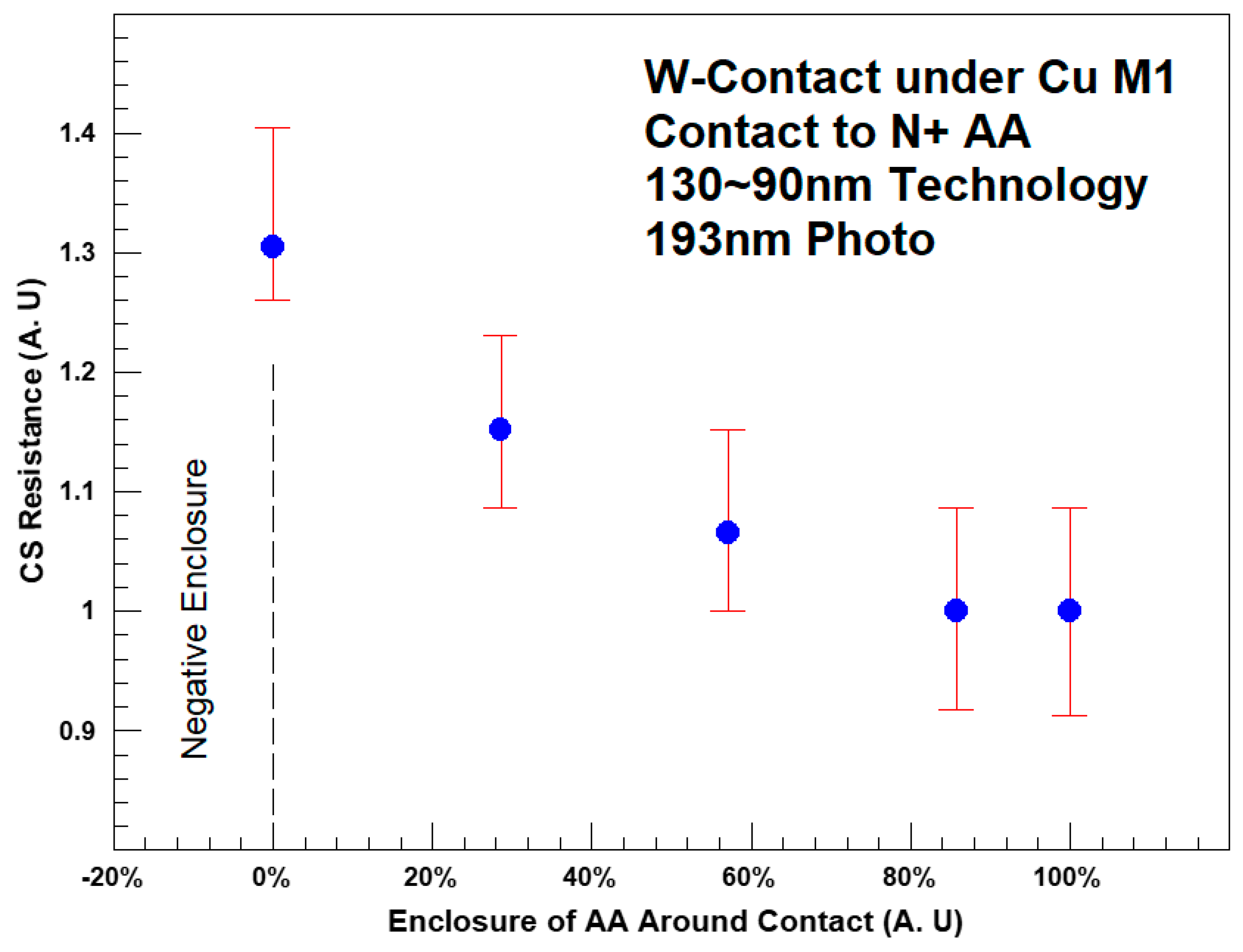
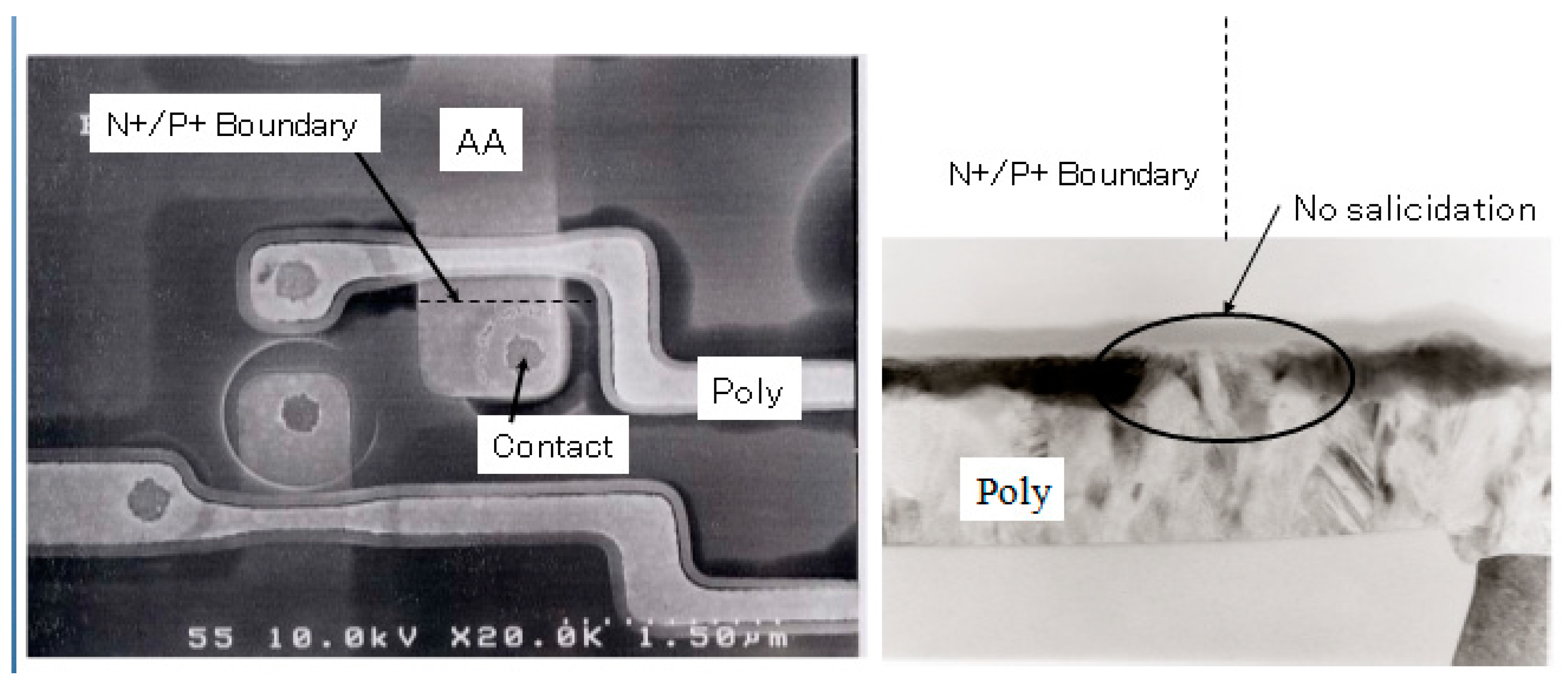
3.2. Enclosure and Extension of Active and Poly around Contact
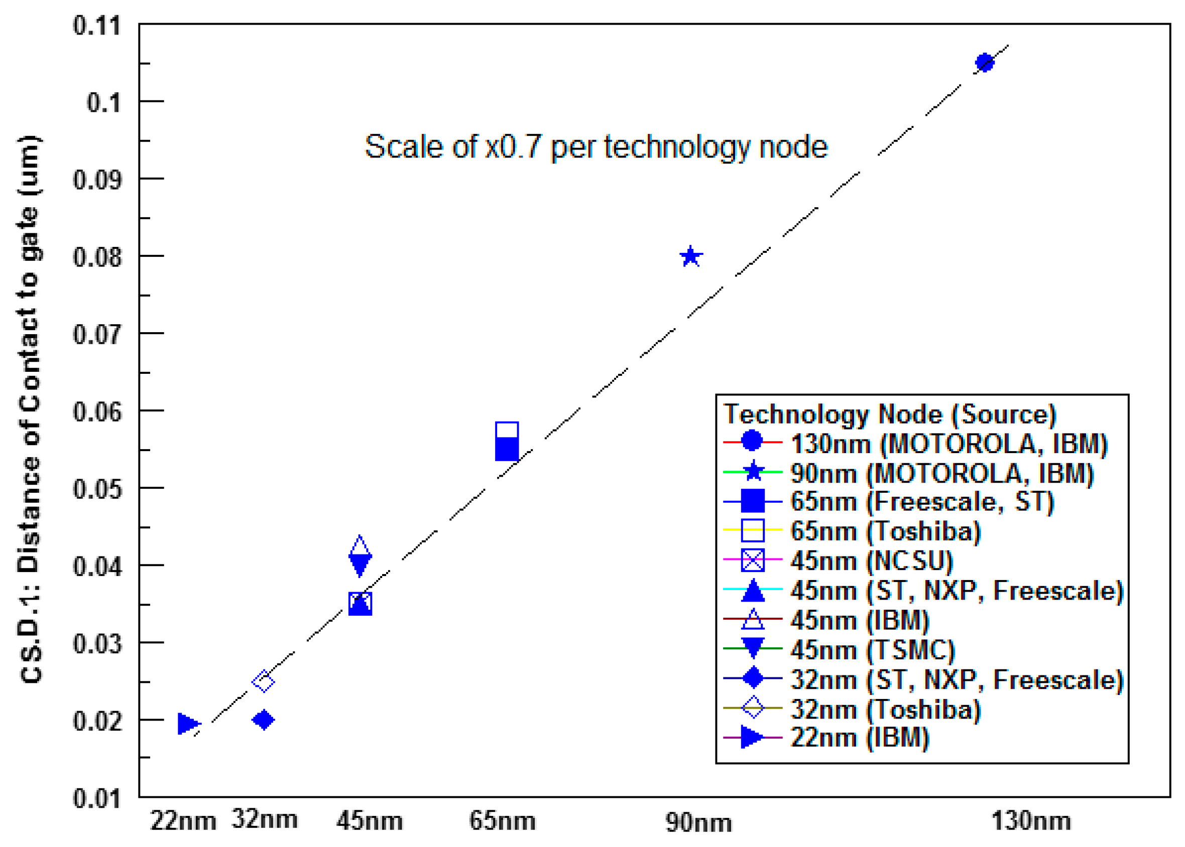
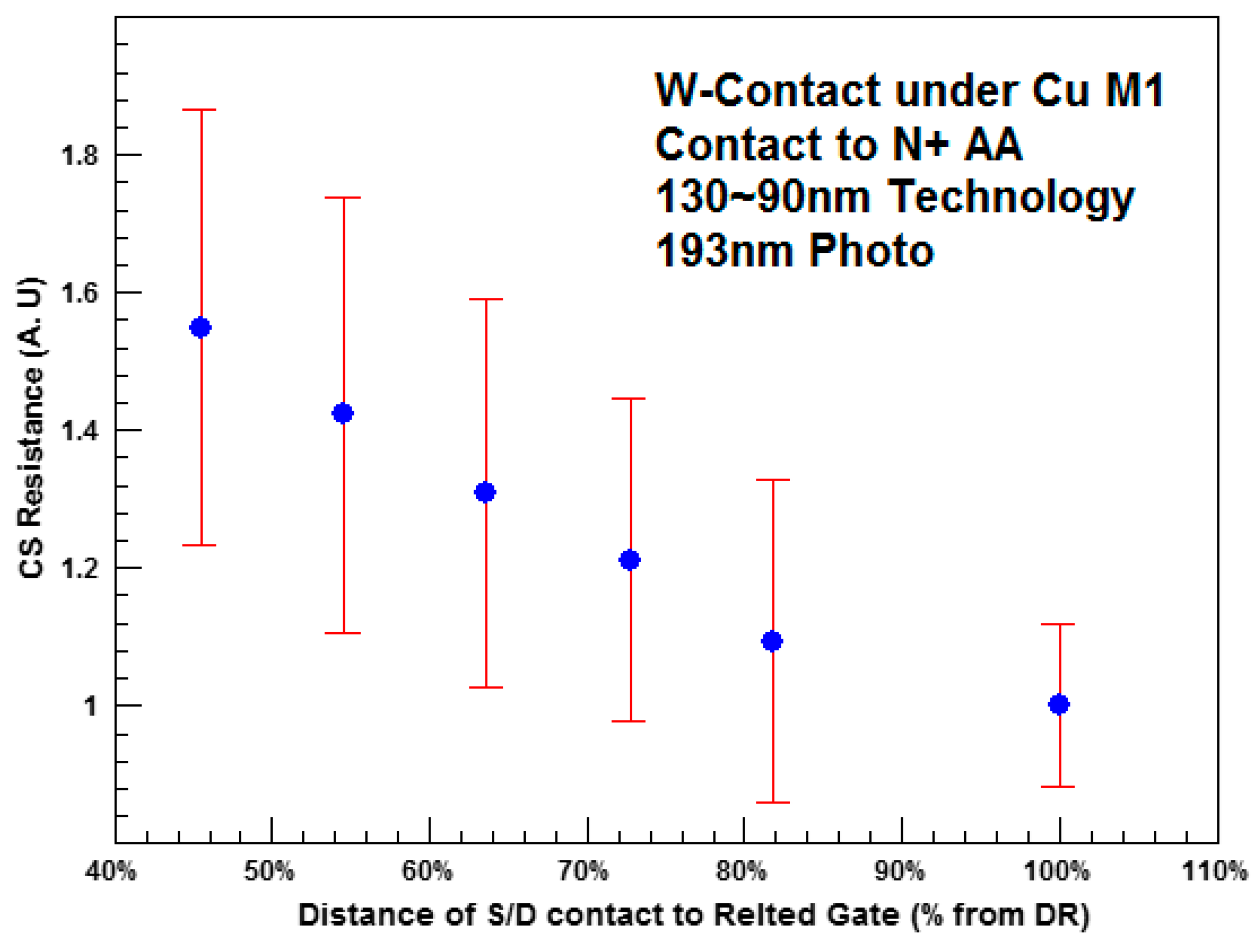
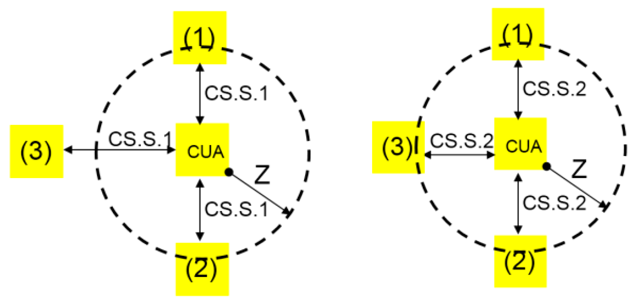
3.3. Distance of S/D Contact to Related Gate (CS.D.1)
- (1)
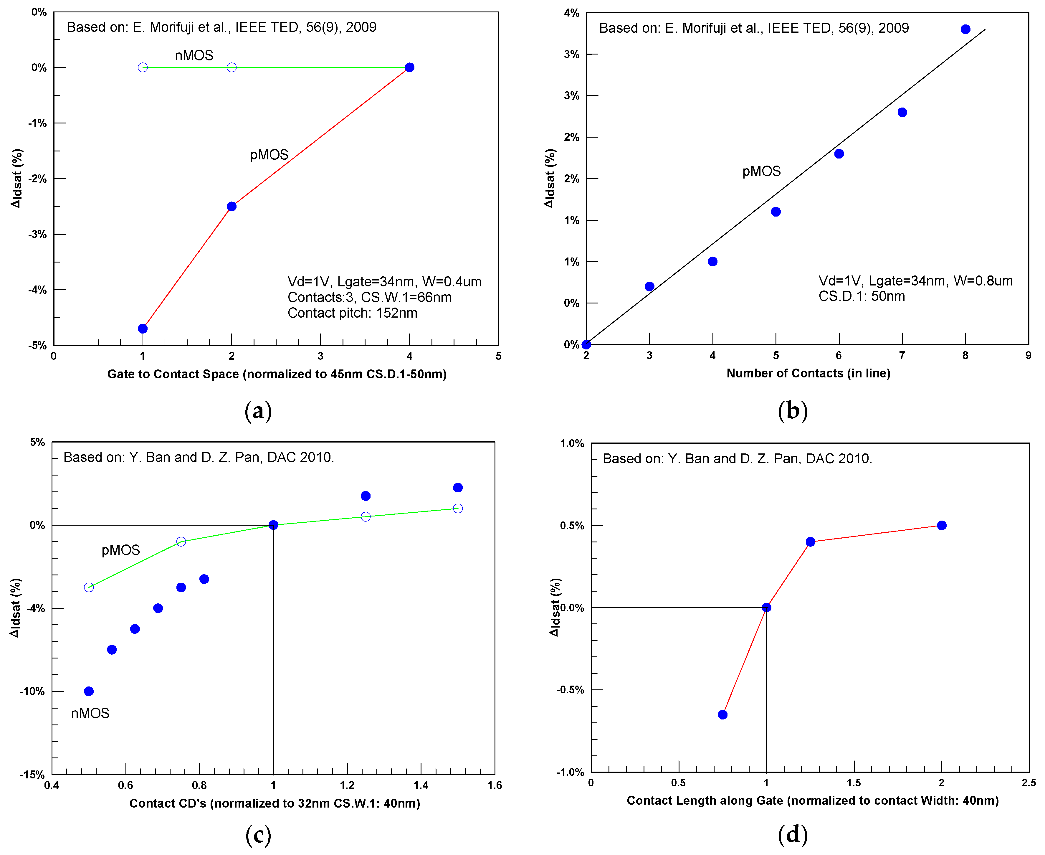
- The distance of S/D contacts to related gate: the larger the distance of the contacts from the gate, the lower is the effective relaxation they induce into the stressed layer [30].In most cases, stress enhance techniques for the nMOSFET used a tensile stressed liner made of nitride that also used as the soft contact etch stop layer (cESL). For the pMOSFET, a compressive linear, together with embedded SiGe (eSiGe), was used (see for example [16,31]). Placing a contact over the S/D area means “punching” the stressed layer, which gives local relaxation to the stress. The closer the contact’sto the related gate (smaller CS.D.1), the higher the effect of the stress relaxation. Due to the fact that the mobility modulation was much higher on pMOSFET when compared to nMOSFET, the effect of pMOSFET was much higher.
- (2)
- Number and the overall area of contacts located between poly gates: a larger number of contacts results in more relaxation of the cESL stress. The contact shape (for the same area) also had an influence. In this case, the current variation of nMOSFET was due to CD variation (area variation), and was found to be more sensitive to that of pMOSFET because of the different resistance dependence [16]. The contact shape was also an important parameter; as the contact length along the gate line was larger (for the same contact area), the saturation current was increased. The main reason was that longer contacts (parallel to the gate) with the same contact area yielded less current crowding from the S/D electric field with similar stress relaxation of the liner [16].For many years, a common guideline for all the technologies recommended the insertion of “double contact” or “redundant contacts” or “as many contacts possible, w/o violating the layout DR’s”. However, for 65 nm technologies and below, which extensively use different types of stressors, such a guideline needs to be modified. New rules and guidelines that specifically define the number of S/D contacts as a function of the transistor width were listed and coded. This is most important for the S/D contact in PMOSFET core that included the eSiGe that does not have a perfect planarity. The P-cell used during design should specify the exact location (CS.D.1) and number of contacts with exact pitch. In addition, during the LPE (layout parameters extraction) step at the design flow, more layout information, including the exact S/D contacts location, was extracted.
- (3)
- Poly pitch: the larger the poly pitch, the higher the stress induced to the channel by the cESL layer until reaching saturation [28]. This stress was not uniform along the poly space and increased toward the center. For nMOSFET, the larger the Poly–Poly space, the higher the mobility enhancement until saturation was reached. However, the overall enhancement was limited to ~5% for 45 nm and <~2% for 20 nm [29]. For pMOSFET, a tight poly space also reduced the enhancement induced from the cESL. In addition, the smaller eSiGe volume also reduced the stress in the channel. The performance enhancement for pMOSFET was ~12% and 10% for 45 nm [13] and 20 nm [29], respectively.
3.4. Non-Square Contacts
3.5. Optical Proximity Correction for Contacts
4. Metal Related Rules
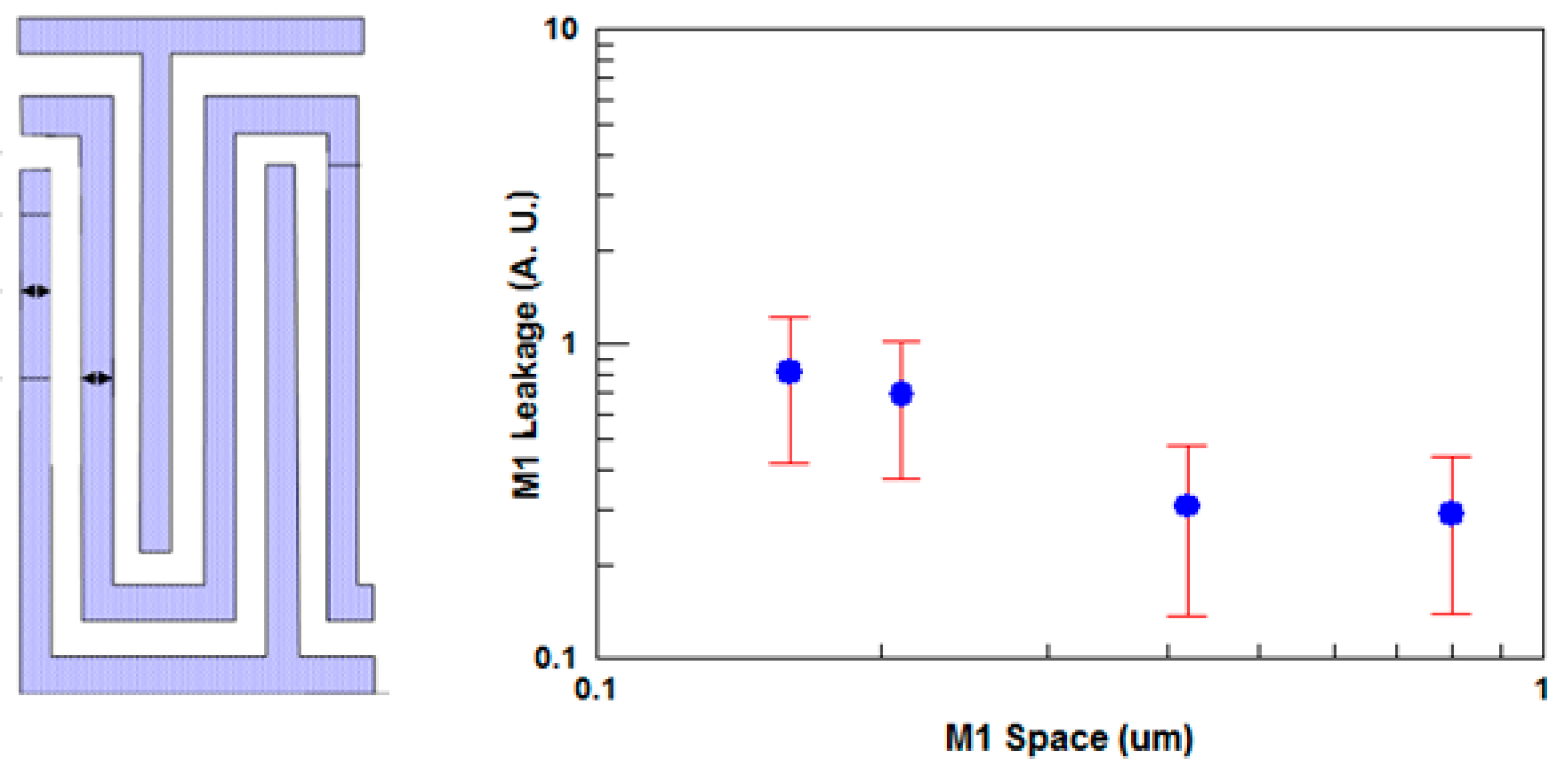
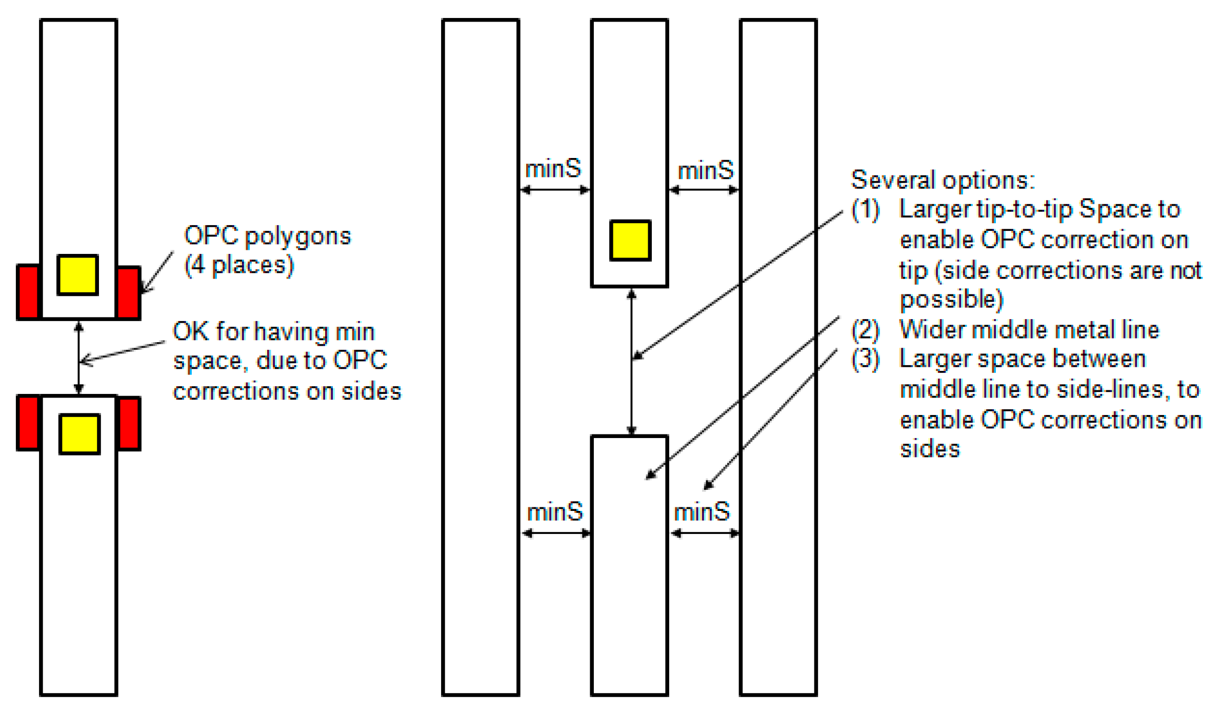
4.1. Metal Width and Space Rules
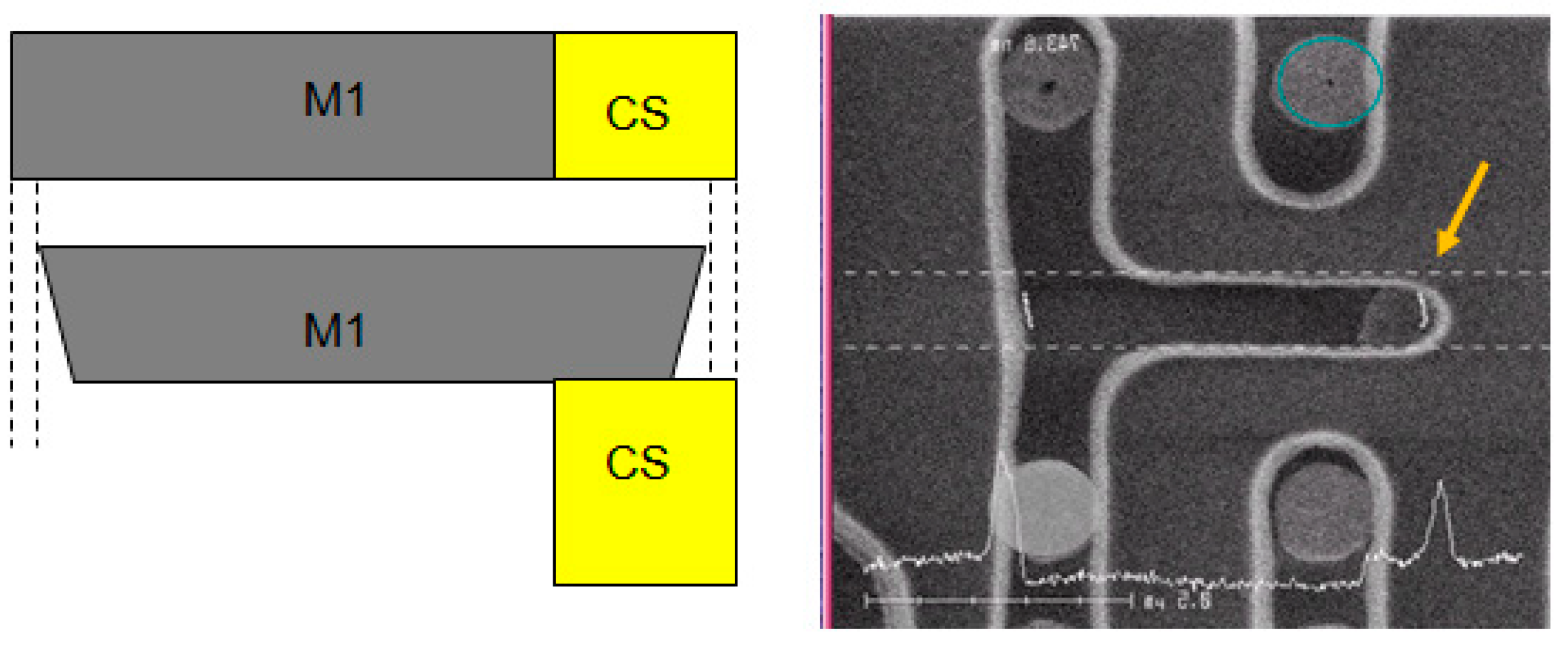
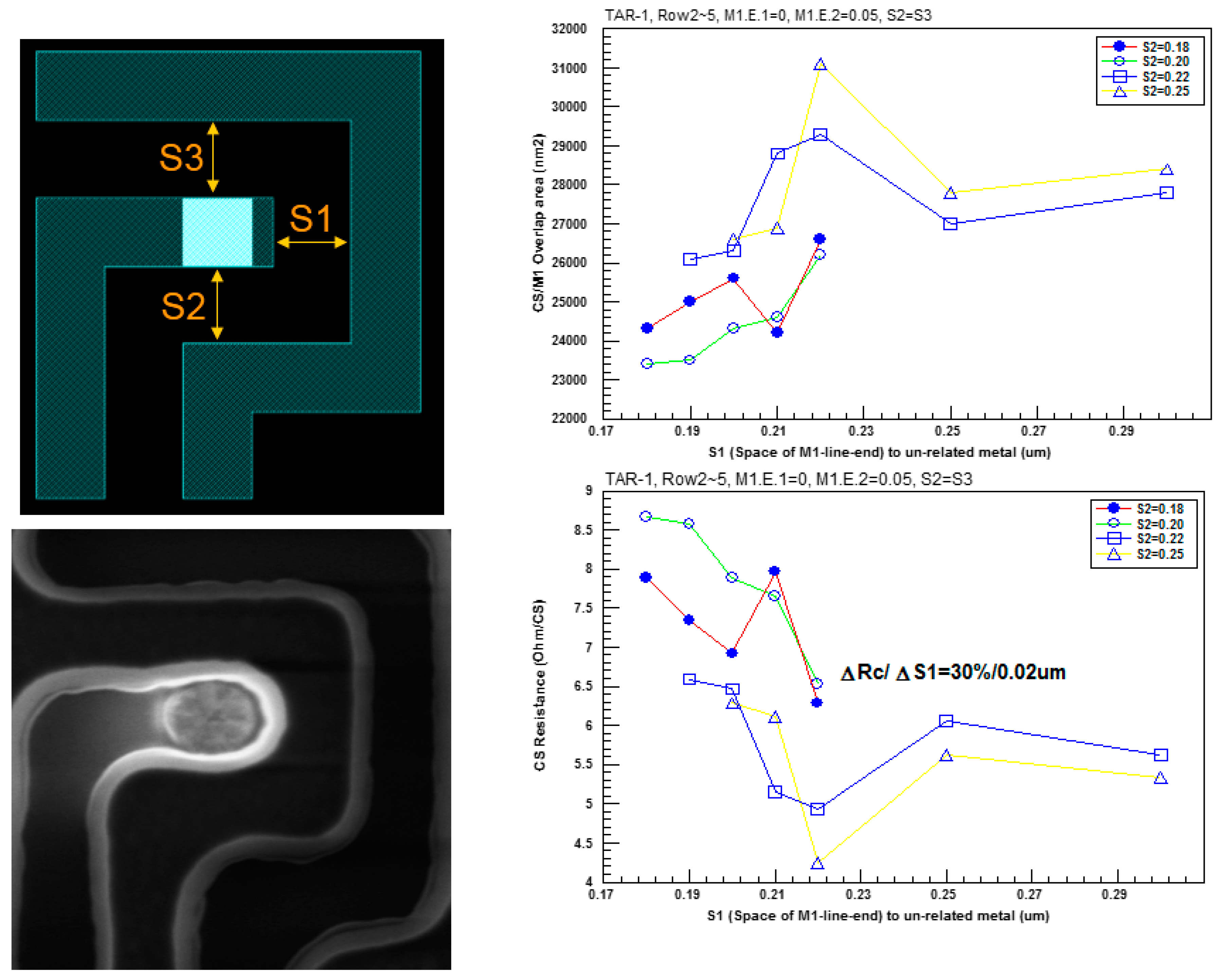
4.2. Metal Enclosed Rules
5. Via Rules
5.1. Via Width and Space Rules
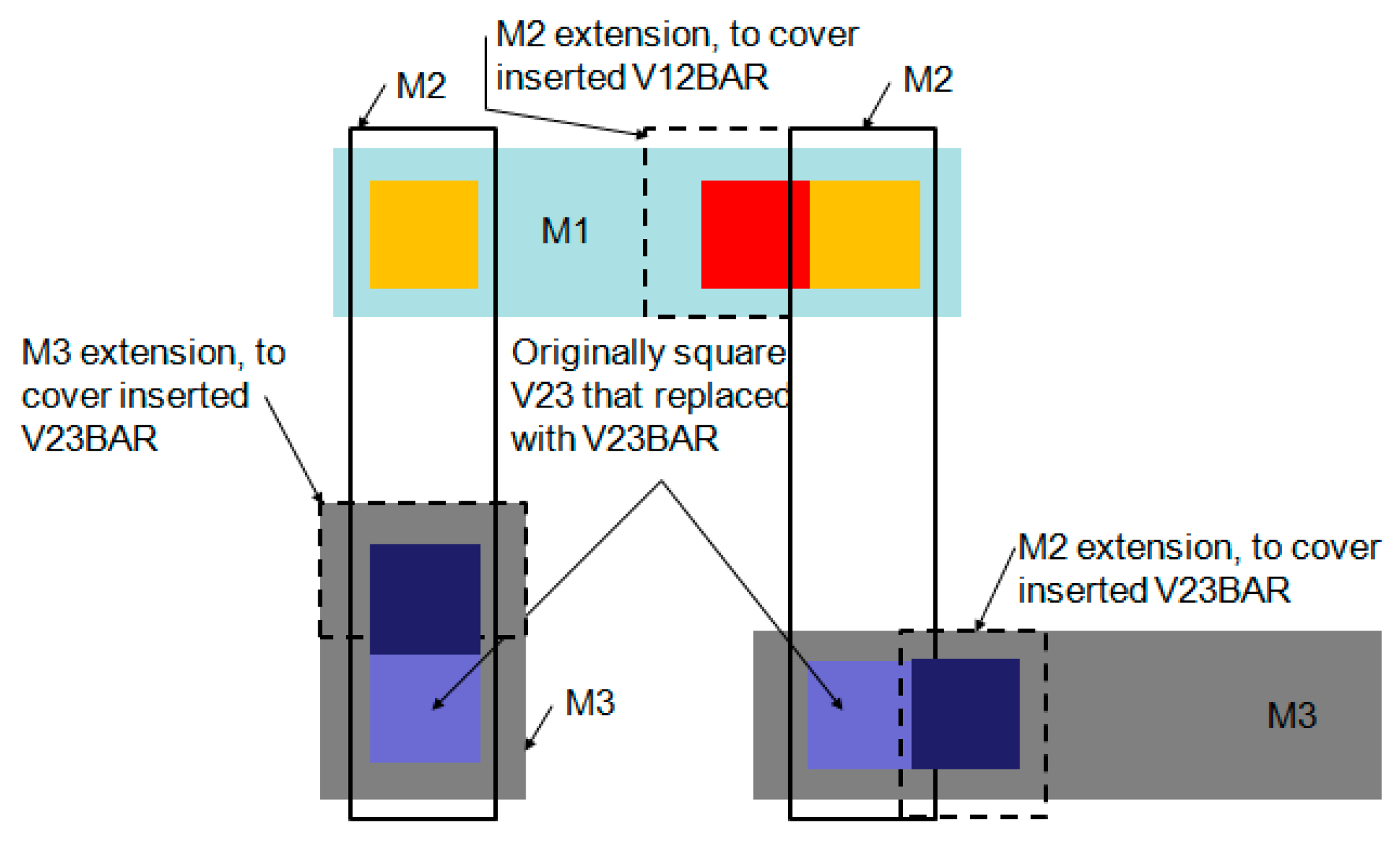
5.2. Double Via and VIABAR Rules
- Step-1:
- Mapping of the different nets, and finding out all square single vias (“lonely via”),
- Step-2:
- Replacing the square via with VIABAR,
- Step-3:
- Checking for structure validity. For example, that the VIABAR is not too close to another via. In case of a violation, go back one step, and change via placing,
- Step-4:
- Ensuring coverage of the metal below/above over the VIABAR. This step is done, by stretching some of the metal (Figure 19),
- Step-5:
- Checking for structure validity. For example, the stretched metal may cause Mx.S.1 violation. In case of a violation, do not stretch the metal and go back to Step 1.
6. BEOL Reliability Related Design Rules
- (1)
- EM tests check the maximum current allowed to pass through a metal line or metal interface (CS/M1 for example). The lifetime (LT) or mean time to failure (MTF) is a function of width, temperature, and the current applied [62]. After analysis, this value was set as the design guideline and included in the design manual.
- (2)
- Stress migration (SM) tests check for any abnormal shift in metal line resistance due to stress generated from the IMD around. These results are used to set up rules related to the number of vias needed to connect two metal lines based on stress induced voids (SIV [63]), failure that is discussed in detail later.
- (3)
- (4)
- After qualification, the data for SM and IMD-TDDB are no longer needed as design guidelines or “rules”, unless the application requires overdrive conditions such as higher maximum temperature or maximum voltage applied.
6.1. Maximum Current Density in Metal Wires and Holes under DC Conditions
6.2. Setting-Up Design Guidelines for Metal Width on the Basis of EM Failures
7. Design Verification
8. BEOL: Next Generation for Materials, Processes, and Related DRs
9. Summary
Funding
Acknowledgments
Conflicts of Interest
References
- Baklanov, R.M.; Ho, P.S.; Zschech, E. (Eds.) Advanced Interconnects for ULSI Technology; Wiley and Sons Publication; John Wiley & Sons, Ltd.: Hoboken, NJ, USA, 2012. [Google Scholar]
- Hau-Riele, C.S. An introduction to Cu electromigration. Microelectron. Reliab. 2004, 44, 195–205. [Google Scholar] [CrossRef]
- Havemann, R.H.; Hutchby, J.A. High-Performance Interconnects: An Integration Overview. Proc. IEEE 2001, 89, 586–601. [Google Scholar] [CrossRef]
- Ishmaru, K. 45 nm/32 nm CMOS—Challanges and perspective. In Proceedings of the 33rd European Solid State Circuits Conference, Munich, Germany, 11–13 September 2007; pp. 1266–1273. [Google Scholar]
- Sun, J.Y.-C. System scaling and collaborative open innovation. In Proceedings of the 2013 Symposium on VLSI Technology, Kyoto, Japan, 11–13 June 2013; pp. T2–T7. [Google Scholar]
- Yoda, T.; Miyajima, H. Advanced BEOL technology overview. In Advanced Nanoscale ULSI Interconnects: Fundamental and Applications; Shacham-Diamand, Y., Osaka, T., Datta, M., Ohba, T., Eds.; Springer: New York, NY, USA, 2009. [Google Scholar]
- Doong, K.Y.-Y.; Ting, J.K.; Hsieh, S.; Lin, S.C.; Shen, B.; Guo, J.C.; Young, K.L.; Chen, I.C.; Sun, J.Y.C.; Wang, J.K. Scaling variance, invariance and prediction of design rule: From 0.25 um to 0.10 um nodes in the era of foundry manufacturing. In Proceedings of the IEEE International Workshop on Statistical Methodology, Kyoto, Japan, 10 June 2001; pp. 38–42. [Google Scholar]
- Doong, K.Y.-Y.; Huang, C.-H.; Chung, C.-C.; Lin, S.-C.; Hung, L.-J.; Ho, S.P.-S.; Hseieh, S.; Wang, R.C.-J.; Lin, P.C.-C.; Kang, R.W.-L.; et al. Infrastructure Development and Integration of Electrical-Based Dimensional Process Window Checking. IEEE Trans. Semiconduct. Manuf. 2004, 17, 123–141. [Google Scholar] [CrossRef]
- Doong, K.Y.-Y.; Hseieh, S.; Lin, S.C.; Hung, L.J.; Wang, R.J.; Shen, B.; Hisa, J.W.; Guo, J.C.; Chen, I.C.; Young, K.L.; et al. As Assessment of physical and electrical design rule based statistical process monitoring and modeling (PEDR-SPMM): For Foundry Manufacturing Line of Multiple-Product-Mixed-Run. In Proceedings of the 2002 International Conference Microelectronic Test Structures, Cork, Ireland, 11 April 2002; pp. 55–59. [Google Scholar]
- Kong, W.; Venkatraman, R.; Castagnetti, R.; Duan, F.; Ramesh, S. High-density and high-performance 6T-SRAM for system-on-Chip in 130 nm CMOS Technology. In Proceedings of the VLSI Symposium on VLSI Technology, Kyoto, Japan, 12–14 June 2001. [Google Scholar]
- Takao, Y.; Nakai, S.; Horiguchi, N. Extended 90 nm CMOS technology with High Manufacturability for High-Performance, Low-Power, RF/Analog Applications. FUJITSU Sci. Tech. J. 2003, 39, 32–39. [Google Scholar]
- Utsumi, K.K.; Morifuji, E.; Kanda, M.; Aota, S.; Yoshida, T.; Honda, K.; Matsubara, Y.; Yamada, S.; Matsuoka, F. A 65 nm Low Power CMOS Platform with 0.495 um2 SRAM for Digital Processing and Mobile Applications. In Proceedings of the VLSI Symposium on VLSI Technology, Kyoto, Japan, 14–16 June 2005. [Google Scholar]
- Morifuji, E.; Aikawa, H.; Yoshimura, H.; Sakata, A.; Ohta, M.; Iwai, M.; Matsuoka, F. Layout dependence modeling for 45-nm CMOS with stress-enhanced technique. IEEE Trans. Electron. Device 2009, 56, 1991–1998. [Google Scholar] [CrossRef]
- NCSU FreePDK45. Available online: www.eda.ncsu.edu/wiki/FreePDK45:Contents (accessed on 21 February 2018).
- Ban, Y.; Ma, Y.; Levinson, H.J.; Deng, Y.; Kye, J.; Pan, D.Z. Modeling and characterization of contact-edge roughness for minimizing design and manufacturing variations in 32-nm node standard cell. Proc. SPIE 2010, 7641. [Google Scholar]
- Ban, Y.; Pan, D.Z. Compact modeling and robust layout optimization for contacts in deep sub-wavelength lithography. In Proceedings of the 2010 47th ACM/IEEE Design Automation Conference (DAC), Anaheim, CA, USA, 13–18 June 2010; p. 408. [Google Scholar]
- Wu, S.-Y.; Liaw, J.J.; Lin, C.Y.; Chiang, M.C.; Yang, C.K.; Cheng, J.Y.; Tsai, M.H.; Liu, M.Y.; Wu, P.H.; Chang, C.H.; et al. A highly manufacturable 28 nm CMOS low power platform technology with fully functional 64Mb SRAM using dual/tripe gate oxide process. In Proceedings of the 2009 Symposium on VLSI Technology, Kyoto, Japan, 16–18 June 2009; pp. 88–89. [Google Scholar]
- Shauly, E.N. CMOS Leakage and Power Reduction in Transistors and Circuits: Process and Layout Considerations. J. Low Power Electron. Appl. 2012, 2, 1–29. [Google Scholar] [CrossRef]
- Shauly, E.N.; Rotstein, I.; Schwarzband, I.; Edan, O.; Levi, S. Monitoring and Characterization of Metal-over-Contact Based Edge-contour Extraction Measurement Followed by Electrical Simulation. Proc. SPIE 2010, 7638, 793810. [Google Scholar]
- Parihar, S.; Angyal, M.; Boeck, B.; Reber, D.; Singhal, A.; van Gompel, T.; Li, R.; Wilson, B.; Wright, M.; Chen, J.; et al. A high density 0.10 µm CMOS technology using low K dielectric and copper interconnect. In Proceedings of the 2001 International Electron Devices Meeting, Washington, DC, USA, 2–5 December 2001. [Google Scholar]
- Mueller, J.; Thoma, R.; Demircan, E.; Bernicot, C.; Juge, A. Modeling of MOSFET parasitic capacitances, and their impact on circuit performance. Solid State Electron. 2007, 51, 1485–1493. [Google Scholar] [CrossRef]
- Fenouillet-Beranger, C.; Denorme, S.; Icard, B.; Boeuf, F.; Coignus, J.; Faynot, O.; Brevard, L.; Buj, C.; Soonekindt, C.; Todeschini, J.; et al. Fully-Depleted SOI Technology using High-K and Single-Metal Gate for 32 nm Node LSTP Applications featuring 0.179 µm2 6T-SRAM bitcell. In Proceedings of the IEEE International Electron Devices Meeting (IEDM 2007), Washington, DC, USA, 10–12 December 2007. [Google Scholar]
- Li, J.; Wille, W.; Zhao, L.; Teo, L.; Dyer, T.; Fang, S.; Yan, J.; Kwon, O.; Kwon, O.; Park, D.; et al. High performance transistors featured in an aggressively scaled 45nm bulk CMOS Technology. In Proceedings of the VLSI Symposium on VLSI Technology, Kyoto, Japan, 12–14 June 2007. [Google Scholar]
- Cheng, K.; Wu, C.C.; Wang, Y.P.; Lin, D.W.; Chu, C.M.; Tarng, Y.W.; Lu, S.Y.; Yang, S.J.; Hsieh, M.H.; Liu, C.M.; et al. A Highly Scaled, High Performance 45 nm Bulk Logic CMOS Technology with 0.242 µm2 SRAM Cell. In Proceedings of the IEEE International Electron Devices Meeting (IEDM 2007), Washington, DC, USA, 10–12 December 2007; pp. 243–246. [Google Scholar]
- Hasegawa, S.; Kitamura, Y.; Takahata, K.; Okamoto, H.; Hirai, T.; Miyashita, K.; Ishida, T.; Aizawa, H.; Aota, S.; Azuma, A.; et al. A cost-conscious 32 nm CMOS platform technology with advanced single exposure lithography and gate-first metal Gate/High-k process. In Proceedings of the IEEE International Electron Devices Meeting (IEDM 2008), San Francisco, CA, USA, 15–17 December 2008. [Google Scholar]
- Haran, B.S.; Kumar, A.; Adam, L.; Chang, J.; Basker, V.; Kanakasabapathy, S.; Horak, D.; Fan, S.; Chen, J.; Faltermeier, J.; et al. 22 nm Technology Compatible Fully Functional 0.1 μm2 6T-SRAM Cell. In Proceedings of the IEEE International Electron Devices Meeting (IEDM 2008), San Francisco, CA, USA, 15–17 December 2008. [Google Scholar]
- King, M.C.; Chin, A. New test structure to monitor contact-to-poly leakage in sub-90 nm CMOS technologies. IEEE Trans. Semiconduct. Manuf. 2008, 21, 244–247. [Google Scholar] [CrossRef]
- Yokogawa, S.; Uno, S.; Kato, I.; Tsuchiya, H.; Shimizu, T.; Sakamoto, M. Statistics of breakdown field and time-dependent dielectric breakdown in contact-to-poly modules. In Proceedings of the 2011 IEEE International Reliability Physics Symposium (IRPS), Monterey, CA, USA, 10–14 April 2011; pp. 149–154, 76410D. [Google Scholar]
- Sato, F.; Ramachandran, R.; van Meer, H.; Cho, K.H.; Ozbek, A.; Yang, X.; Liu, Y.; Li, Z.; Wu, X.; Jain, S.; et al. Process and Local Layout Effect interaction on a high performance planar 20 nm CMOS. In Proceedings of the 2013 Symposium on VLSI Technology, Kyoto, Japan, 11–13 June 2013; Volume 56. [Google Scholar]
- Liebmann, R.; Nawaz, M.; Bach, K.H. Efficient 2D approximation for Layout-dependent Relaxation of Etch Stop Liner Stress due to Contact Holes. In Proceedings of the 2006 International Conference on Simulation of Semiconductor Processes and Devices (SISPAD), Monterey, CA, USA, 6–8 September 2006; pp. 6–8. [Google Scholar]
- Wang, C.-C.; Zhao, W.; Liu, F.; Chen, M.; Cao, Y. Modeling of layout-dependent stress effect in CMOS design. In Proceedings of the IEEE/ACM International Conference on Computer-Aided Design—Digest of Technical Papers (ICCAD’09), San Jose, CA, USA, 2–5 November 2009; p. 513. [Google Scholar]
- Levin, M.; Heng, F.L.; Northop, G. Backend CAD Flows for “Restrictive Design Rules”. In Proceedings of the IEEE/ACM International Conference on Computer Aided Design (ICCAD 2004), San Jose, CA, USA, 7–11 November 2004; pp. 739–746. [Google Scholar]
- Arora, R.; Seth, S.; Poh, J.C.H.; Cressler, J.D.; Sutton, A.K.; Nayfeh, H.M.; Rosa, G.L.; Freeman, G. Impact of Source/Drain Contact and Gate Finger Spacing on the RF Reliability of 45-nm RF nMOSFETs. In Proceedings of the IEEE International Reliability Physics Symposium, Monterey, CA, USA, 10–14 April 2011; pp. 461–466. [Google Scholar]
- Fournier, D.; Ducatteau, D.; Fontaine, J.; Scheer, P.; Bon, O.; Rauber, B.; Buczko, M.; Gloria, D.; Gaquiere, C.; Chevalier, P. Improvement of the RF Power Performance of nLDMOSFETs on Bulk and SOI Substrates with “Ribon” Gate and Source contacts layouts. In Proceedings of the 21st International Symposium on Power Semiconductor Devices & IC’s, Barcelona, Spain, 14–18 June 2009. [Google Scholar]
- Cheng, K.; Khakifirooz, A. Fully depleted SOI (FDSOI) technology. Sci. China Inf. Sci. 2016, 59, 1–15. [Google Scholar] [CrossRef]
- Morgenfeld, B.; Stobert, I.; Haffner, H.; An, J.; Kanai, H.; Ostermayr, M.; Chen, N.; Aminpur, M.; Brodsky, C.; Thomas, A. Strategies for single patterning of contacts for 32 nm and 28 nm technology. In Proceedings of the 2011 22nd Annual IEEE/SEMI Advanced Semiconductor Manufacturing Conference (ASMC), Saratoga Springs, NY, USA, 16–18 May 2011. [Google Scholar]
- Wang, C.-H.; Liu, Q.; Zhang, L.; Hung, C.-Y. No-forbidden-pitch SRAF rules for advanced contact lithography. Proc. SPIE 2006, 6349. [Google Scholar] [CrossRef]
- Gupta, T. Copper Interconnect Technology; Springer: New York, NY, USA, 2009. [Google Scholar]
- Ciofi, I.; Roussel, P.J.; Saad, Y.; Moroz, V.; Hu, C.-Y.; Baert, R.; Croes, K.; Contino, A.; Vandersmissen, K.; Gao, W.; et al. Modeling of Via Resistance for Advanced Technology Nodes. IEEE Trans. Electron Devices 2017, 64, 2306–2313. [Google Scholar] [CrossRef]
- Mistry, K.; Allen, C.; Auth, C.; Beattie, B.; Bergstrom, D.; Bost, M.; Brazier, M.; Buehler, M.; Cappellani, A.; Chau, R.; et al. A 45 nm Logic Technology with High-k+Metal Gate Transistors, Strained Silicon, 9 Cu Interconnect Layers, 193 nm Dry Patterning, and 100% Pb-free Packaging. In Proceedings of the IEEE International Electron Devices Meeting (IEDM 2007), Washington, DC, USA, 10–12 December 2007; pp. 247–250. [Google Scholar]
- Natarajan, S.; Armstrong, M.; Bost, M.; Brain, R.; Brazier, M.; Chang, C.-H.; Chikarmane, V.; Childs, M.; Deshpande, H.; Dev, K.; et al. A 32 nm logic technology featuring 2nd-Generation High-k+Metal-Gate transistors, enhanced channel strain and 0.171 μm2 SRAM Cell Size in a 291Mb Array. In Proceedings of the 2008 IEEE International Electron Devices Meeting, San Francisco, CA, USA, 15–17 December 2008; pp. 941–943. [Google Scholar]
- Kitada, H.; Suzuki, T.; Kimura, T.; Kudo, H.; Ochimizu, H.; Okano, S.; Tsukune, A.; Suda, S.; Sakai, S.; Ohtsuka, N.; et al. The Influence of the Size Effect of Copper Interconnect on RC Delay Variability Beyond 45 nm Technology. In Proceedings of the IEEE International Interconnect Technology Conference (IEEE 2007), Burlingame, CA, USA, 4–6 June 2007; pp. 10–12. [Google Scholar]
- Hegde, G.; Bowen, R.C.; Rodder, M.S. Lower Limits of Line Resistance in Nanocrystalline Back End of line Cu Interconnects. Appl. Phys. Lett. 2016, 109, 193106. [Google Scholar] [CrossRef]
- Aubel, O.; Gall, M. BEOL reliability challenges and its interaction with process integration. In Proceedings of the Tutorial in International Reliability Physics Symposium, Waikoloa, HI, USA, 1–5 June 2014. [Google Scholar]
- Aubel, O.; Hennesthal, C.; Hauschildt, M.; Beyer, A.; Poppe, J.; Talut, G.; Gall, M.; Hahn, J.; Boemmels, J.; Nopper, M.; et al. Backend-of-Line Reliability Improvement Options for 28 nm Node Technologies and Beyond. In Proceedings of the 2011 IEEE International Interconnect Technology Conference and 2011 Materials for Advanced Metallization (IITC/MAM), Dresden, Germany, 8–12 May 2011; pp. 1–3. [Google Scholar]
- Chiang, C.C.; Kawa, J. Design for Manufacturability and Yield for Nano-Scale CMOS; Springer: Cham, The Netherlands, 2007. [Google Scholar]
- Mentor Graphics. Yield Analyzer. Available online: http://www.mentor.com (accessed on 13 May 2018).
- Abrecrombie, D.; Ferguson, J. Equation-Based DRC: A Novel Approach to Resolving Complex Nanometer Design Issues. Available online: http://bbs.hwrf.com.cn/downpcbe/1-TP2--David_Abercrombie_John_Ferguson-7143.pdf (accessed on 13 May 2018).
- Shi, X.; Socha, B.; Bendik, J.; Dusa, M.; Conley, W.; Su, B. Experimental Study of Line End Shortening. Proc. SPIE 1999, 3678. [Google Scholar] [CrossRef]
- Yang, J.; Capodieci, L.; Sylvester, D. Layout Verification and Optimization based on Flexible Design Rules. Proc. SPIE 2006, 6156. [Google Scholar] [CrossRef]
- Azzoni, P.; Bertoletti, M.; Dragone, N.; Fummi, F.; Guardiani, C.; Vendraminetto, W. Yield-aware Placement Optimization. In Proceedings of the Design, Automation & Test in Europe Conference & Exhibition, Nice, France, 16–20 April 2007. [Google Scholar]
- Alagna, P.; Zurita, O.; Rechtsteiner, G.; Lalovic, I.; Bekaert, J.P. Improving On-wafer CD Correlation Analysis Using Advanced Diagnostics and Across-wafer Light-source Monitoring. Proc. SPIE 2014, 9052, 905228. [Google Scholar] [CrossRef]
- Veendrick, H.J.M. Nanometer CMOS ICs; Springer: Berlin, Germany, 2017. [Google Scholar]
- Ludwing, C.; Meyer, S. Double Patterning for Memory ICs. Available online: https://www.intechopen.com/books/recent-advances-in-nanofabrication-techniques-and-applications (accessed on 13 May 2018).
- Kawasaki, H.; Lee, C.; Pintchovski, F. The Effect of Test Structure and stress Condition on electromigration failure. In Proceedings of the Symposium on Reliability of Metals in Electronics; The Electrochemical Society, Inc.: Pennington, NJ, USA, 1995; pp. 165–177. [Google Scholar]
- Liu, W.; Lim, Y.K.; Tan, J.B.; Zhang, W.Y.; Liu, H.; Siah, S.Y. Study of TDDB reliability in misaligned via chain structures. In Proceedings of the 2012 IEEE International Reliability Physics Symposium (IRPS), Anaheim, CA, USA, 15–19 April 2012. [Google Scholar]
- Inohara, M.; Tamura, I.; Yamaguchi, T.; Koike, H.; Enomoto, Y.; Arakawa, S.; Watanabe, T.; Ide, E.; Kadomura, S.; Sunouchi, K. High performance Copper and Low-k interconnect technology fully compatible to 90 nm-node SOC application (CMOS4). In Proceedings of the International IEDM, Electron Devices Meeting (IEDM '02), San Francisco, CA, USA, 8–11 December 2002. [Google Scholar]
- Okuno, M.; Okabe, K.; Sakuma, T.; Suzuki, K.; Miyashita, T.; Yao, T.; Morioka, H.; Terahara, M.; Kojima, Y.; Watatani, H.; et al. 45-nm node CMOS integration with a novel STI structure and full-NCS/Cu interlayers for low-operation-power (lop) applications. In Proceedings of the IEEE International Electron Devices Meeting IEDM Technical Digest, Washington, DC, USA, 5 December 2005; pp. 52–55. [Google Scholar]
- Chatterjee, A.; Yoon, J.; Zhao, S.; Tang, S.; Sadra, K.; Crank, S.; Mogul, H.; Aggarwal, R.; Chatterjee, B.; Lytle, S.; et al. A 65 nm CMOS technology for mobile and digital signal processing applications. In Proceedings of the IEEE International Electron Devices Meeting (IEDM 2004), San Francisco, CA, USA, 13–15 December 2004. [Google Scholar]
- Schiml, T.; Biesemans, S.; Brase, G.; Burrell, L.; Cowley, A.; Chen, K.C.; Ehrenwall, A.V.; Ehrenwall, B.V.; Felsner, P.; Gill, J.; et al. A 0.13 µm CMOS Platform with Cu/Low-k Interconnects for System on Chip Applications. In Proceedings of the 2001 International Symposium on VLSI Technology, Kyoto, Japan, 18–20 April 2001; Volume 12, pp. 2000–2001. [Google Scholar]
- Sardin, P. Via Redundancy improvement using ViaBAR features in 28 nm CMOS custom layout. In Proceedings of the Mentor Graphics U2U Meeting, Santa Clara, CA, USA, 12 April 2012. [Google Scholar]
- JEDEC Publication. Standard Method for Calculating the Electromigration Model Parameters for Current Density and Temperature; JESD63; JEDEC: Arlington, VA, USA, 1998. [Google Scholar]
- Ogawa, E.T.; McPherson, J.W.; Rosal, J.A.; Dickerson, K.J.; Chiu, T.; Tsung, L.Y.; Jain, M.K.; Bonifield, T.D.; Ondrusek, J.C.; McKee, W.R. Stress-induced voiding under-vias connected to wide Cu metal leads. In Proceedings of the IEEE 40th Annual International Reliability Physics Symposium Proceedings, Dallas, TX, USA, 7–11 April 2002; pp. 312–321. [Google Scholar]
- McPherson, J.W. Reliability Physics and Engineering, Time-to-Failure-Modeling; Springer: New York, NY, USA, 2010. [Google Scholar]
- Croes, K.; Wu, C.; Kocaay, D.; Li, Y.; Roussell, P.; Bommels, J.; Toki, Z. Current Understanding of BEOL TDDB Lifetime models. ECS J. Solid-State Sci. Technol. 2015, 4, N3094–N3097. [Google Scholar] [CrossRef]
- Ohring, M. Reliability and Failure of Electronic Materials and Devices; Academic Press: New York, NY, USA, 1998. [Google Scholar]
- Llyod, J.R.; Rodbell, K.P. Reliability. In Handbook of Semiconductor Interconnection Technology, 2nd ed.; Schwartz, G.C., Srikrishman, K.V., Eds.; CRC Press: New York, NY, USA, 2006. [Google Scholar]
- JEDEC/FSA Joint Publication. Foundry Process Qualification Guidelines (Wafer Fabrication Manufacturing Sites); JP001.01; JEDEC: Arlington, VA, USA, 2014. [Google Scholar]
- AEC-Q100. Failure Mechanism Based Stress Test Qualification for Integrated Circuits. Available online: http://www.aecouncil.com/index.html (accessed on 13 May 2018).
- Kuper, F. Reliability qualification strategies. In Proceedings of the IEEE International Reliability Physics Symposium (IRPS), Waikoloa, HI, USA, 1–5 June 2014. [Google Scholar]
- Vairagar, A.V.; Mhaisalkar, S.G.; Krishnamoorthy, A. Electromigration Behavior of Dual-damascene Cu Interconnects—Structure, Width, and Length Dependencies. Microelectron. Reliab. 2004, 44, 747–754. [Google Scholar] [CrossRef]
- Lin, M.H.; Lin, Y.L.; Chang, K.P.; Su, K.C.; Wang, T. Copper Interconnect Electromigration Behaviors in Various Structures and Life Time Improvement by Cap/Dielectric Interface Treatment. Microelectron. Reliab. 2005, 45, 1061–1078. [Google Scholar] [CrossRef]
- Aubel, O. BEOL Reliability Challenges and Its Interaction with Process Integration. In Proceedings of the IEEE International Reliability Physics Symposium, Monterey, CA, USA, 10–14 April 2011. [Google Scholar]
- Oates, A.S.; Lin, M.H. The Impact of trench width and barrier thickness on scaling of the electromigration short—Length effect in Cu/Low-k interconnects. In Proceedings of the 2013 IEEE International Reliability Physics Symposium (IRPS), Anaheim, CA, USA, 14–18 April 2013. [Google Scholar]
- Cheng, Y.L.; Lin, B.L.; Lee, S.Y.; Chiu, C.C.; Wu, K. Cu Interconnect width effect, mechanism and resolution on down-stream electromigration. In Proceedings of the IEEE 45th Annual International Reliability Physics Symposium, Phoenix, AZ, USA, 15–19 April 2007; pp. 128–133. [Google Scholar]
- Ko, T.; Chang, C.L.; Chou, S.W.; Lin, M.W.; Lin, C.J.; Shin, C.H.; Su, H.W.; Tsai, M.H.; Shue, W.S.; Liang, M.S. High performance/reliability Cu interconnects with selective CoWP cap. In Proceedings of the 2003 VLSI Symposium on VLSI Technology, Kyoto, Japan, 10–12 June 2003. [Google Scholar]
- Lin, M.H.; Lin, M.T.; Wang, T. Effects of Length Scaling on Electromigration in Dual-Damascene Copper Interconnects. Microelectron. Reliab. 2008, 48, 569–577. [Google Scholar] [CrossRef]
- Lee, K.-D.; Ogawa, E.T.; Yoon, S.; Lu, X.; Ho, P.S. Electromigration reliability of dual-damascene Cu/porous methylsilsesquioxane low-k interconnects. Appl. Phys. Lett. 2003, 82, 2032–2034. [Google Scholar] [CrossRef]
- Seo, S.; Yang, C.-C.; Wang, M.; Monsieur, F.; Adam, L.; Johnson, J.B.; Horak, D.; Fan, S.; Cheng, K.; Stathis, J.; et al. Copper Contact for 22 nm and Beyond: Device Performance and Reliability Evaluation. IEEE Electron Device Lett. 2010, 31, 1452–1454. [Google Scholar] [CrossRef]
- Seo, S.; Yang, C.-C.; Yeh, C.; Haran, B.; Horak, D.; Fan, S.; Koburger, C.; Canaperi, D.; Rao, S.S.P.; Monsieur, F.; et al. Copper Contact metallization for 22 nm and beyond. In Proceedings of the IEEE International Interconnect Technology Conference (IITC 2009), Sapporo, Hokkaido, Japan, 1–3 June 2009; pp. 8–10. [Google Scholar]
- Van der Veen, M.H.; Vandersmissen, K.; Dictus, D.; Demuynck, S.; Liu, R.; Bin, X.; Nalla, P.; Lesniewska, A.; Hall, L.; Croes, K.; et al. Cobalt bottom-up contact and via prefill enabling advanced logic and DRAM technologies. In Proceedings of the 2015 IEEE International Interconnect Technology Conference and 2015 IEEE Materials for Advanced Metallization Conference (IITC/MAM), Grenoble, France, 18–21 May 2015; pp. 25–28. [Google Scholar]
- Morris, J. IEDM 2017: GlobalFoundries Announces 7 nm Chipmaking Process. Available online: https://www.zdnet.com/article/iedm-2017-globalfoundries-announces-7nm-chipmaking-process/ (accessed on 13 December 2017).
- Hu, C.; Kelly, J.; Huang, H.; Motoyama, K.; Shobha, H.; Ostrovski, Y.; Chen, J.H.; Patlolla, R.; Peethala, B.; Adusumilli, P.; et al. Future on-chip interconnect metallization and electromigration. In Proceedings of the 2018 IEEE International Reliability Physics Symposium (IRPS), Burlingame, CA, USA, 11–15 March 2018. [Google Scholar]


| Rule Code | Rule Description | Action | 130 nm | 90 nm | 65 nm | 45 nm | 28 nm |
|---|---|---|---|---|---|---|---|
| CS.W.1 | Contact width | exact | 0.15 [10] | 0.12 [11] | 0.09 [12] | 0.06 [13]; 0.065 [14] | 0.04 [15] |
| CS.S.1 | Contact space (same net) | min | 0.19 [10] | 0.14 [11] | 0.11 [12] | 0.08 [13]; 0.075 [14] | 0.07 [16] |
| Rule Code | Rule Description | Action | 130 nm | 90 nm | 65 nm | 45 nm | 32/28 nm |
|---|---|---|---|---|---|---|---|
| M1.Th | M1 (local) Thickness (nm) | ~ 400 | ~0.35 | ~0.24 | 144 [40] | 95 [41] | |
| M1.Diel | M1 Inter-Metal Dielectric (Type, k) | LK, 3.0 [23] | |||||
| M1.W.1 | Width of M1 | min | 0.16 [10] | 0.12 [11] | 0.09 [12] | 0.065 [23] | 0.05 [25] |
| M1.S.1 | Space of M1 | min | 0.18 [10] | 0.12 [11] | 0.09 [12] | 0.065 [23] | 0.05 [25] |
| MI.Th | MI (Intermediate) Thickness (nm) | ~450 | ~0.35 | ~0.24 | 144 [40] | 95 [41] | |
| MI.Diel | MI Inter-Metal Dielectric (Type, k) | ULK, 2.4 [23] | |||||
| MI.W.1 | Width of MI | min | 0.20 [10] | 0.14 [11] | 0.10 [12] | 0.14 [23] | 0.10 [25] |
| MI.S.1 | Space of MI | min | 0.20 [10] | 0.14 [11] | 0.10 [12] | 0.14 [23] | 0.10 [25] |
| MZ.Th | MZ (Semi-Global) Thickness (nm) | 504 [40] | |||||
| MZ.Diel | MZ Inter-Metal Dielectric (Type, k) | LK, 3.0 [23] | |||||
| MZ.W.1 | Width of MZ | min | 0.28 [11] | 0.28 [23] | |||
| MZ.S.1 | Space of MZ | min | 0.28 [11] | 0.28 [23] | |||
| ML.Th | ML (Global) Thickness (nm) | 720 [40] | 504 [41] | ||||
| ML.Diel | ML Inter-Metal Dielectric (Type, k) | USG, 4.2 | USG, 4.2 | USG, 4.2 | FSG, 3.65 [23] | ||
| ML.W.1 | Width of ML | min | ~0.40 | 0.42 [11] | 0.40 [23] | ~0.28 [41] | |
| ML.S.1 | Space of ML | min | ~0.40 | 0.42 [11] | 0.40 [23] | ~0.28 [41] | |
| MF.Th | MF (Fat) Thickness (nm) | ~3 µm | ~3 µm | ~3 µm | ~3 µm | ~3 µm | |
| MF.Diel | MF Inter-Metal Dielectric (Type, k) | USG, 4.2 | USG, 4.2 | USG, 4.2 | USG, 4.2 | USG, 4.2 | |
| MF.W.1 | Width of MF | min | ~2 µm | ~2 µm | ~2 µm | ~2 µm | ~2 µm |
| MF.S.1 | Space of MF | min | ~2 µm | ~2 µm | ~2 µm | ~2 µm | ~2 µm |
| Rule Code | Rule Description | Action | 130 nm | 90 nm | 65 nm | 45 nm | 32/28 nm |
|---|---|---|---|---|---|---|---|
| VI.W.1 | Width of Vi (Intermediate) | min | 0.18 [10] | 0.14 [57] | 0.10 [12] | 0.07 [58] | 0.05 [25] |
| VI.S.1 | Space of Vi (Intermediate) | min | 0.18 [10] | 0.14 [57] | 0.10 [12] | 0.07 [58] | 0.07 [25] |
| VZ.W.1 | Width of VZ (Semi-Global) | min | 0.28 [57] | 0.18 [59] | 0.14 [58] | 0.10 [25] | |
| VZ.S.1 | Space of VZ (Semi-Global) | min | 0.28 [57] | 0.27 [59] | 0.14 [58] | 0.10 [25] | |
| VL.W.1 | Width of VL (Global) | min | 0.40 [60] | 0.60 [57] | 0.36 [59] | 0.42 [58] | |
| VL.S.1 | Space of VL (Global) | min | 0.40 [60] | 0.60 [57] | 0.49 [59] | 0.42 [58] | |
| VF.W.1 | Width of VF (Top) | min | 0.50 [58] | ||||
| VF.S.1 | Space of VF (Top) | min | 1.18 [58] |
| Platform (Node) | Layer and Thickness (nm) | JDC_max at 110 °C (mA/um) |
|---|---|---|
| 130~90 nm | ~0.9 um | ~6 |
| 65~55 nm | ~1.2 um | ~9 |
| 45~40 nm | ~1.5 um | ~9 |
© 2018 by the author. Licensee MDPI, Basel, Switzerland. This article is an open access article distributed under the terms and conditions of the Creative Commons Attribution (CC BY) license (http://creativecommons.org/licenses/by/4.0/).
Share and Cite
Shauly, E.N. Physical, Electrical, and Reliability Considerations for Copper BEOL Layout Design Rules. J. Low Power Electron. Appl. 2018, 8, 20. https://doi.org/10.3390/jlpea8020020
Shauly EN. Physical, Electrical, and Reliability Considerations for Copper BEOL Layout Design Rules. Journal of Low Power Electronics and Applications. 2018; 8(2):20. https://doi.org/10.3390/jlpea8020020
Chicago/Turabian StyleShauly, Eitan N. 2018. "Physical, Electrical, and Reliability Considerations for Copper BEOL Layout Design Rules" Journal of Low Power Electronics and Applications 8, no. 2: 20. https://doi.org/10.3390/jlpea8020020
APA StyleShauly, E. N. (2018). Physical, Electrical, and Reliability Considerations for Copper BEOL Layout Design Rules. Journal of Low Power Electronics and Applications, 8(2), 20. https://doi.org/10.3390/jlpea8020020