
Analysis and Implementation of a Frequency Control DC–DC Converter for Light Electric Vehicle Applications

Department of Electrical Engineering, National Yunlin University of Science and Technology, Yunlin 640, Taiwan
Electronics 2021, 10(14), 1623; https://doi.org/10.3390/electronics10141623
Submission received: 24 June 2021
/
Revised: 5 July 2021
/
Accepted: 6 July 2021
/
Published: 7 July 2021
(This article belongs to the Special Issue 10th Anniversary of Electronics: Related Researches in Electrical and Autonomous Vehicles)
Abstract
:In order to realize emission-free solutions and clean transportation alternatives, this paper presents a new DC converter with pulse frequency control for a battery charger in electric vehicles (EVs) or light electric vehicles (LEVs). The circuit configuration includes a resonant tank on the high-voltage side and two variable winding sets on the output side to achieve wide output voltage operation for a universal LEV battery charger. The input terminal of the presented converter is a from DC microgrid with voltage levels of 380, 760, or 1500 V for house, industry plant, or DC transportation vehicle demands, respectively. To reduce voltage stresses on active devices, a cascade circuit structure with less voltage rating on power semiconductors is used on the primary side. Two resonant capacitors were selected on the resonant tank, not only to achieve the two input voltage balance problem but also to realize the resonant operation to control load voltage. By using the variable switching frequency approach to regulate load voltage, active switches are turned on with soft switching operation to improve converter efficiency. In order to achieve wide output voltage capability for universal battery charger demands such as scooters, electric motorbikes, Li-ion e-trikes, golf carts, luxury golf cars, and quad applications, two variable winding sets were selected to have a wide voltage output (50~160 V). Finally, experiments with a 1 kW rated prototype were demonstrated to validate the performance and benefits of presented converter.
1. Introduction
Clean renewable energies with power electronic techniques have been widely developed to generate alternative current (AC) voltage or direct current (DC) voltage on AC utility systems [1,2,3,4] or DC microgrid systems [5,6]. Normally, DC/DC pulse-width modulation converters (PWMs) and AC/DC PWM converters are adopted for solar power [7,8] and wind power [9] applications to convert unstable DC and AC voltage into a stable DC voltage on DC nanogrid or microgrid systems. The DC bus voltage on a DC microgrid may be 380, 760, or 1500 V for residential houses, light rail vehicles, or DC traction vehicles applications, respectively. DC–DC converters [10,11,12,13] with full bridge circuit topologies have been developed to convert low voltage (380 V) input into low voltage units (5, 12, or 48 V) for computers, server systems, light electric vehicle (LEVs), or telecommunication applications. Three level or multilevel converters [14,15,16] have been proposed for medium voltage (760 V) or high voltage (1500 V) input applications. Soft switching converters were researched in [17,18,19,20,21,22] to decrease switching losses on power semiconductors and high efficiency. Active clamp pulse-width modulation (PWM) and asymmetric PWM techniques were studied in [17,18] to improve the switching loss from half rated power to full power by adding an extra inductor on the primary side of a DC/DC PWM converter. However, the main problems of asymmetric PWM converters are unbalanced voltages and current stresses on power devices. Using the phase shift PWM technique on full bridge converters [19,20] can reduce switching loss and obtain a high circuit efficiency. The main disadvantage of phase shift PWM techniques is the hard switching problem on the lagging-leg switches. Resonant converters with the pulse frequency modulation technique were presented in [21,22] to realize low switching losses on power semiconductors over the whole load range. However, the main drawback of resonant converters is their narrow input voltage range.
To implement clean transportation alternatives and realize emission-free demands, a new PWM converter with the advantages of a wide voltage output capability and low switching loss is presented and verified in this paper for a universal battery charger in LEV or electric vehicle (EV) applications. A cascade resonant circuit was selected to lessen the voltage rating on active devices so that 600 V power switches are adopted for the 760 V input condition. Two resonant capacitors are used on the resonant tank to not only achieve resonant behavior but also input spilt voltage balance. Due to the variable switching frequency, active devices are turned on under zero voltage switching (ZVS), and the fast recovery diodes are turned off under zero current switching (ZCS). Therefore, the power losses are reduced in the presented converter. To implement the wide voltage output capability for universal battery charger applications in LEV or EV systems, two winding sets were selected for the low voltage side to have different voltage gains under high or low output voltage regions. The presented circuit has a more concise circuit configuration, less device counts, and an easier control strategy when using the general purpose PWM integrated circuit compared to the conventional DC converters. The basic DC microgrid system and the circuit configuration of the presented converter are provided in Section 2. The circuit operation for wide voltage operation capability is discussed in Section 3. The circuit analysis of the studied converter is provided in Section 4. Section 5 gives the design procedures and experiments of the presented circuit. In Section 6, the conclusion and future work directions are provided.
2. Circuit Configuration
The basic circuit blocks of DC nanogrid or microgrid systems are illustrated in Figure 1. The input voltages on a DC microgrid can be DC or AC voltage from clean renewable energies such as wind power and photovoltaic (PV) power or utility systems. Therefore, the AC/DC or DC/DC PWM converters need to change unstable AC voltage from wind turbine generators or unstable DC voltage from PV panels to stable DC voltage on DC microgrid systems. Bidirectional AC/DC or DC/DC PWM converters are needed between utility and DC microgrid systems to achieve bidirectional power flow capability. DC microgrids can supply AC motor drives, energy storage units, light rail transit systems, or battery chargers for LEVs through DC/AC inverters or DC/DC converters. The input voltage of DC transportation applications is 750 or 1500 V. However, the input voltage of a residential house or a local industry factory is 380, ±380, or 760 V. Therefore, the DC bus voltage on DC microgrids can be 380, ±380, 760, or 1500 V for different power rating requirements. High voltage PWM converters are normally adopted to supply the high power output for EV chargers or DC transportation systems.
Figure 2 provides a circuit diagram of the studied high voltage DC/DC converter. The input voltage is 760 V from the DC bus of the DC microgrid. The output voltage of the studied converter is used to charge batteries for LEV applications such as scooters, electric motorbikes, Li-ion e-trikes, golf carts, luxury golf cars, and quads. Due to the wide battery voltage range in LEV applications, DC/DC converters need to have wide output voltage operation capabilities. Figure 2a provides a diagram of the presented circuit with Vin = 760 V and Vo = 50 V–160 V. Four active devices, two input capacitors, an isolated transformer, a resonant inductor, and two resonant capacitors are used on the high voltage side (primary side). Four fast recovery diodes, an active switch, an output capacitor, and a DC resistor are adopted on the low voltage side (secondary side). Due to the series connection of four active devices on the high voltage side, active devices with a 600 V voltage rating are adopted on the primary side to withstand 760 V input. The series resonant circuit structure with Lr, Cr1, Cr2, and Lm is adopted on the presented converter to have the advantage of a soft switching operation for active devices (S1–S4) and fast recovery diodes (D1–D4). Two center-taped rectifiers with different winding turns are used on the low voltage side to extend the output voltage range operation. If switch S5 is OFF (Figure 2b), D1 and D4 are OFF. The low voltage output is provided in the proposed converter with ns secondary winding turns. The voltage gain at the low voltage output condition (Figure 2b) is Vo/Vin = G(fsw)ns/(4np), where G(fsw) is the voltage gain of the series resonant circuit. If switch S5 is ON (Figure 2c), D2 and D3 are OFF and the high voltage output is provided in the proposed converter with 2ns secondary winding turns. Therefore, the voltage gain at the high voltage output condition is Vo/Vin = G(fsw)ns/(2np). Thus, the studied converter can provide a low (high) voltage output range with S5 OFF (ON).
3. Circuit Operation
To realize the wide output voltage operation, the presented circuit has two equivalent sub-circuits, as shown in Figure 2b,c. S1–S4 are controlled with pulse switching frequency modulation (PFM). For low and high output voltage ranges, the switching signals and the main voltage and current waveforms are provided in Figure 3a,b, respectively. For the low voltage output range, the studied converter is only operated at a low voltage gain. Therefore, S5 is off, and D1 and D4 are also off. In order to generate the square voltage PWM waveforms on leg voltages vab and vbc, the gate waveforms of S1 (S2) and S3 (S4) are identical. If the proposed converter is used at the switching frequency fsw < (or >) series resonant frequency fr,1 by Cr1, Cr2, and Lr, the presented resonant converter has six (or four) working modes in every switching cycle. Figure 4 shows the equivalent working modes under fsw < fr,1. If the converter is operated at fsw > fr,1, then only modes 1, 3, 4, and 6 are used in the proposed converter for every switching period.
Mode 1 [t0 ~ t1]: vCS1 = vCS3 = 0 at time t0. Due to iCS3 < 0 and iCS1 < 0, the body diodes DS3 and DS1 are naturally conducting. The ZVS turn-on of S3 and S1 is accomplished at t0. The capacitor voltage vCr2 + vCr1 = Vdc1. Due to iLr (t) > iLm(t), the fast recovery diode D2 is conducting and vLm = (np/ns)Vo. Lr, Cr2, and Cr1 are resonant in mode 1 with resonant frequency where Cr = Cr1 = Cr2.
Mode 2 [t1 ~ t2]: since fr,1 < fsw, iD2 will decrease to 0 at t1. Then, D1 becomes off without reverse recovery current loss. On the primary side, Lm, Lr, Cr2, and Cr1 are naturally resonant with the resonant frequency .
Mode 3 [t2 ~ t3]: S1 and S3 are turned off at t2, and CS2 and CS4 are discharged. After time t2, iLm > iLr such that D3 is conducting and vLm becomes −(np/ns)Vo. The magnetizing current iLm(t2) can be obtained as follows:
The ZVS condition of S4 and S2 is given as:
where Coss = CS1 = CS2 = CS3 = CS4. However, the dead time td between S2 and S1 must be greater than the discharged time of CS2 and CS4. Therefore, the maximum value of Lm can be obtained as follows:
Mode 4 [t3 ~ t4]: at t3, vCS2 = vCS4 = 0. The body diodes DS4 and DS2 are naturally forward-biased. The ZVS turn-on of S4 and S2 is achieved. Due to iLr(t3) < iLm(t3), the fast recovery diode D3 is conducting and vLm = −(np/ns)Vo. Lr, Cr2, and Cr1 are naturally resonant on the primary side in mode 4.
Mode 5 [t4 ~ t5]: at time t4, iD3 = 0. Thus, D3 becomes off. Lm, Lr, Cr2, and Cr1 are naturally resonant on the primary side with the resonant frequency fr,2.
Mode 6 [t5 ~ Tsw+t0]: S2 and S4 turn off at t5, and CS1 and CS3 are discharged. After time t5, iLm < iLr such that D2 becomes forward-biased and vLm = (np/ns)Vo. At time t0 + Tsw, vCS1 = vCS3 = 0.
For the high voltage output range, the studied converter has a high voltage gain. S5 is turned on, and the fast recovery diodes D2 and D3 are reverse-biased. The presented converter has six (or four) operating modes in every switching cycle if fsw < (or >) fr,1. Figure 5 provides the equivalent circuits for fsw < fr,1.
Mode 1 [t0 ~ t1]: at time t0, vCS1 = vCS3 = 0. DS1 and DS3 are conducting, vS2,ds = vS4,ds = Vin/2, and vCr1 + vCr2 = Vin/2. D1 is conducting so that vLm = npVo/(2ns).
Mode 2 [t1 ~ t2]: if fr,1 > fsw, the iD1 will be decreased to 0 at t1. Then, D1 is off.
Mode 3 [t2 ~ t3]: at t2, S1 and S3 turn off. Due to iLr < iLm, the fast recovery diode D4 becomes forward-biased and vLm = −npVo/(2ns). The magnetizing current iLm(t2) can be obtained as follows:
The ZVS condition of S4 and S2 for the high voltage output region is obtained as follows:
In order to have ZVS operation, the maximum value of Lm for the high voltage output region is given as follows:
Mode 4 [t3 ~ t4]: at t3, vCS2 = vCS4 = 0. DS4 and DS2 become forward-biased. Due to iLm > iLr, the fast recovery diode D4 becomes forward-biased and vLm = −npVo/(2ns).
Mode 5 [t4 ~ t5]: if fr,1 > fsw, the iD4 will be decreased to 0 at time t4. Then, D4 becomes reverse-biased.
Mode 6 [t5 ~ Tsw+t0]: at time t5, S4 and S2 are turned off. Due to iLr > iLm after time t5, the fast recovery diode D1 becomes forward-biased and vLm = npVo/(2ns). At time t0 + Tsw, vCS3 = vCS1 = 0.
4. Circuit Analysis
For the design of the resonant converter, a general pulse frequency modulation was selected to generate the PWM signals for all power switches. Power switch S5 is controlled by using an input voltage comparator to select low (or high) winding turns on the output side under the low (or high) voltage output region. For frequency analysis under frequency modulation, the equivalent AC circuit of the proposed converter on the primary side is given in Figure 6a. In Figure 6a, Vin,e and Re are the equivalent AC input voltage and AC resistor on the primary side, respectively. The voltage Vin,e is a square voltage waveform with voltage values of 0 V and Vin/2. One can obtain the input voltage at fundamental frequency . Components Cr1 and Cr2 are connected in parallel (Cr,eq = Cr1 + Cr2 = 2Cr) under the equivalent AC resonant tank. For the low voltage output range, the turn-ratio of the isolation transformer is np/ns (S5 off). However, the transformer turn-ratio is np/(2ns) under the high voltage output range (S5 on). One can obtain the magnetizing voltage vLm = ±npVo/ns (low voltage output range) or ±npVo/(2ns) (high voltage output range). The magnetizing voltage at the fundamental frequency can be obtained as (or ) for the low output voltage range (or high output voltage range). The equivalent AC resistor Re on the primary side is given as follows:
The voltage transfer function between the output and input sides is given in Equation (8) and shown in Figure 6b.
where , ln = Lm/Lr, and fn = fsw/fr,1. From Equation (8), Vo can be obtained as follows:
5. Design Considerations and Experiments
In this presented converter, the following are the basic input and output electric specifications: Vin = 760 V, Vo = 50~160 V, Po = 1000 W, fr,1 = 100 kHz, and ln = 7.5. For the low voltage output range, Vo = 50~90 V. For the high voltage output range, Vo is between 90 and 160 V. The circuit design procedure is based on the low voltage output range (Vo = 50~90 V). The design voltage gain of the presented converter is unity at fsw = fr,1 with Vin = 760 V and Vo = 50 V. From Equation (8), np/ns can be obtained as follows:
The transformer T is implemented with the ferrite core (TDK EE-55) with Ae = 3.54 cm2 and ΔB = 0.4 T. The assumed minimum switching frequency fsw,min = 60 kHz at Vin = 90 V. The primary turns np,min can be obtained in Equation (11):
In this laboratory prototype, the selected winding turns were np = 32 and ns = 8. Then, DC voltage gains were obtained through Equations (12) and (13):
For the high output voltage range (Vo = 90~160 V), the maximum and minimum DC gains of the presented converter could be obtained as follows:
Under the low output voltage range and the full load condition, Re is given in Equation (16) at Vo = 90 V:
The quality factor x = 0.05 and inductor ratio ln = 7.5 were selected in this design procedure, and Cr1, Cr2, Lr, and Lm could be derived in Equations (17)–(19).
S1–S4 have a voltage stress of 190 V (=Vin,max/4). STF40N60M2 (650 V/22 A) power devices were selected for S1–S4. Die to Vo,max = 160 V, STTH15R06D (600 V/12 A) power diodes were selected for D1–D4. Power switch S5 was chosen to be implemented by 6R070P6 (650 V/33 A). The selected capacitances were Cin1 = Cin2 = 330 μF/450 V and Co = 1360 μF/200 V. The Schmitt voltage comparator with Vf = 90 V was selected to control switch S5 (S5 OFF if Vo ≤ 90 V or S5 ON if Vo > 90 V). The UCC25600 was selected to implement pulse frequency modulation for S1–S4. Table 1 illustrates the circuit parameters in the laboratory prototype. Figure 7 shows a picture of the prototype circuit in the laboratory test.
The experimental results of the proposed converter for low voltage range operation are illustrated in Figure 8 and Figure 9. Figure 8 illustrates the experiments of the presented circuit under Vin = 760 V and Vo = 50 V at a 1 kW load. Figure 8a gives the experimental PWM waveforms of S1–S4. S1 and S3 were found to have the same PWM signals. In the same manner, the PWM signals of S2 and S4 were identical. Figure 8b shows the PWM signal of S1 and leg voltages vab and vbc. If S1 and S3 were on and S2 and S4 were off, then the leg voltages vab = VCdc1 = Vin/2 = 380 V and vbc = 0. When S1 and S3 were off and S2 and S4 were on, the leg voltages vab = 0 and vbc = VCdc2 = Vin/2 = 380 V. Figure 8c illustrates the experimental waveforms of vCr1, vCr2, and iLr. The AC voltage components of vCr1 and vCr2 were found to be complementary to each other, and the voltage value vCr1 + vCr2 = Vin/2. Due to the half bridge type resonant circuit, the DC voltage values vCr1,DC = vCr2,DC = Vin/4 = 190 V. The presented converter at Vo = 50 V had a GDC,min,L = 1.05 theoretical DC voltage gain. The switching frequency was close to the resonant frequency. Therefore, the inductor current iLr was a sinusoidal waveform. Since the presented converter at Vo = 50 V was operated under the low voltage output region, S5 was off and D1 and D4 were reverse-biased. Figure 8d illustrates the experimental waveforms of the secondary-side currents iD2, iD3, and Io and load voltage Vo. The PWM signals of S1 at Po = 200 W (20% load) and 1 kW (100% load) are given in Figure 8e,f, respectively. It can be seen in Figure 8e,f that the active device S1 turned on at ZVS from 20% load to 100% load. In the same manner, the experiments of the presented converter under Vo = 90 V and 1 kW load are illustrated in Figure 9. Following from Equations (12) and (13), the converter at Vo = 90 V output had more voltage gain than at the Vo = 50 V output condition. Thus, the switching frequency in Figure 9a–d (at Vo = 90 V output) was less than the switching frequency in Figure 8a–d (at Vo = 50 V output). For Vo = 90 V output, the theoretical DC voltage gain in Equation (12) was 1.89. Therefore, it could be expected that the switching frequency was less than the series resonant frequency shown in Figure 9c and the fast recovery diodes D2 and D3 could be turned off at the zero current switching shown in Figure 9d. From the experiments shown in Figure 9e,f, it is clear that S1 turned on at ZVS from 20% load to 100% load. Similarly, the experiments of the converter under high voltage range operation are provided in Figure 10 and Figure 11. For the high voltage output operation, S5 was on and D2 and D3 were reverse-biased. Figure 10 and Figure 11 illustrate the experiments for the Vo = 95 and 160 V output and 100% load conditions. Following Equations in (14) and (15), the voltage gain of converter at Vo = 95 V was close to unity and the DC voltage gain at Vo = 160 V was greater than unity. Therefore, the switching frequency of the presented converter at the Vo = 95 V (160 V) output was greater (less) than the resonant frequency. This phenomenon can be observed in Figure 10a–d and Figure 11a–d. For the Vo = 95 V condition, it can be seen that fsw > fr,1. In Figure 10d, the fast recovery diodes D1 and D4 were turned off at hard switching. On the other hand, the switching frequency fsw < fr,1 under the Vo = 160 V output condition. Therefore, D1 and D4 were turned off at zero current switching, as shown in Figure 11d. From the test experiments in Figure 10e,f and Figure 11e,f, it can be seen that S1 was turned off at ZVS from 20% load to full load for both Vo = 95 and 160 V. Since the circuit characteristics of S2, S3, and S4 are the same as S1, it could be expected that S1–S4 had the soft switching turn-on operation. The experiments of output voltage Vo and switch S5 are provided in Figure 12 during the output voltage variation between 50 and 160 V. If the output voltage was less than 90 V, S5 was off (vS5,g = 0 V). On the other hand, S5 was on (vS5,g = 15 V) if Vo > 90 V. The presented converter had 90%, 94%m and 91% efficiencies at Vo = 50, 95, and 160 V, respectively, under the Vin = 760 V and Po = 1 kW conditions. The proposed converter at Vo = 95 V was operated at fsw > fr,1. Therefore, power switches were operated at ZVS turn-on and rectifier diodes were operated at hard switching turn-off. Due to the fsw > fr,1 at the Vo = 95 V condition, the higher switching frequency reduced the magnetizing current loss compared to the Vo = 160 V condition (fsw < fr,1). Therefore, the circuit efficiency at the Vo = 95 V condition was better than Vo = 160 V.
6. Conclusions
A new DC resonant converter is presented and verified in this paper in DC nano- or micro-grid systems with a wide output voltage capability. The main contributions of the presented DC–DC converter are (1) a high input voltage circuit structure that uses a flying capacitor to balance two input capacitor voltages, (2) a wide output voltage operation using a control switch, and (3) a wide ZVS operation range for wide output voltage and load ranges. Since the square voltage waveforms are generated on vab and vbc, the voltage vCr1 + vCr2 = VCdc1 (if S1 and S3 are on) with d = Tsw/2 or VCdc2 (if S2 and S4 are on) with d = Tsw/2. Thus, the flying capacitors Cr1 and Cr2 can be used to balance input capacitor voltages VCdc1 = VCdc2 = Vin/2. To solve the high voltage application problems, a cascade resonant circuit is used on high voltage side to limit the voltage stress on active devices at Vin/2. Therefore, the general purpose power MOSFETs with a 600 V voltage rating can be used in the presented circuit. To realize wide output voltage requirements, such as for battery chargers for universal electric motorcycles or vehicles, the converter has two winding sets to extend the output voltage range using a control switch. In order to lessen the switching losses on active devices and increase the circuit efficiency, a series resonant converter using a LLC circuit structure was adopted for the presented converter to have a ZVS turn-on characteristic on active devices and a possible ZCS turn-off characteristic on fast recovery diodes. Therefore, the proposed converter can achieve soft switching operation from 200 to 1000 W load in the experimental test. Finally, the design procedures and experiments of the prototype circuit are provided to show the circuit performance and effectiveness of the studied converter. Further work on this circuit will consider reducing the number of circuit components and cost, as well as extending the output voltage range for universal battery charging station applications.
Funding
This research is supported by the Ministry of Science and Technology (MOST), Taiwan, under grant number MOST 108-2221-E-224-022-MY2.
Acknowledgments
The author thanks the financial support by the Ministry of Science and Technology, Taiwan, under contract MOST 108-2221-E-224-022-MY2. The author also likes to thank Y.H. Peng for his help to measure and validate the experimental waveforms.
Conflicts of Interest
The author declare no conflict of interest.
References
- He, J.; Yang, Y.; Vinnikov, D. Energy Storage for 1500 V Photovoltaic Systems: A Comparative Reliability Analysis of DC- and AC-Coupling. Energies 2020, 13, 3355. [Google Scholar] [CrossRef]
- Youssef, E.; Costa, P.B.C.; Pinto, S.F.; Amin, A.; El Samahy, A.A. Direct Power Control of a Single Stage Current Source Inverter Grid-Tied PV System. Energies 2020, 13, 3165. [Google Scholar] [CrossRef]
- Yang, M.; Cao, W.; Lin, T.; Zhao, J.; Li, W. Low Frequency Damping Control for Power Electronics-Based AC Grid Using Inverters with Built-In PSS. Energies 2021, 14, 2435. [Google Scholar] [CrossRef]
- Ali, A.I.M.; Sayed, M.A.; Mohamed, A.A.S. Seven-Level Inverter with Reduced Switches for PV System Supporting Home-Grid and EV Charger. Energies 2021, 14, 2718. [Google Scholar] [CrossRef]
- Frivaldsky, M.; Morgos, J.; Prazenica, M.; Takacs, K. System Level Simulation of Microgrid Power Electronic Systems. Electronics 2021, 10, 644. [Google Scholar] [CrossRef]
- Zhang, C.; Li, P.; Guo, Y. Bidirectional DC/DC and SOC Drooping Control for DC Microgrid Application. Electronics 2020, 9, 225. [Google Scholar] [CrossRef] [Green Version]
- Litrán, S.P.; Durán, E.; Semião, J.; Barroso, R.S. Single-Switch Bipolar Output DC-DC Converter for Photovoltaic Application. Electronics 2020, 9, 1171. [Google Scholar] [CrossRef]
- Xiong, X.; Yang, Y. A Photovoltaic-Based DC Microgrid System: Analysis, Design and Experimental Results. Electronics 2020, 9, 941. [Google Scholar] [CrossRef]
- Thayumanavan, P.; Kaliyaperumal, D.; Subramaniam, U.; Bhaskar, M.S.; Padmanaban, S.; Leonowicz, Z.; Mitolo, M. Combined Harmonic Reduction and DC Voltage Regulation of a Single DC Source Five-Level Multilevel Inverter for Wind Electric System. Electronics 2020, 9, 979. [Google Scholar] [CrossRef]
- Kim, D.H.; Kim, M.S.; Nengroo, S.H.; Kim, C.H.; Kim, H.J. LLC Resonant Converter for LEV (Light Electric Vehicle) Fast Chargers. Electronics 2019, 8, 362. [Google Scholar] [CrossRef] [Green Version]
- Mouli, G.R.C.; Duijsen, P.V.; Grazian, F.; Jamodkar, A.; Bauer, P.; Isabella, O. Sustainable E-Bike Charging Station That Enables AC, DC and Wireless Charging from Solar Energy. Energies 2020, 13, 3549. [Google Scholar] [CrossRef]
- Kim, C.-E. Optimal Dead-Time Control Scheme for Extended ZVS Range and Burst-Mode Operation of Phase-Shift Full-Bridge (PSFB) Converter at Very Light Load. IEEE Trans. Power Electron. 2019, 34, 10823–10832. [Google Scholar] [CrossRef]
- Jain, P.; Pahlevaninezhad, M.; Pan, S.; Drobnik, J. A Review of High-Frequency Power Distribution Systems: For Space, Telecommunication, and Computer Applications. IEEE Trans. Power Electron. 2014, 29, 3852–3863. [Google Scholar] [CrossRef]
- Madhusoodhanan, S.; Tripathi, A.; Patel, D.; Mainali, K.; Kadavelugu, A.; Hazra, S.; Bhattacharya, S.; Hatua, K. Solid-State Transformer and MV Grid Tie Applications Enabled by 15 kV SiC IGBTs and 10 kV SiC MOSFETs Based Multilevel Converters. IEEE Trans. Ind. Appl. 2015, 51, 3343–3360. [Google Scholar] [CrossRef]
- Lin, B.-R.; Lu, H.-H. New multilevel rectifier based on series connection of H-bridge cell. IEE Proc. Electr. Power Appl. 2000, 147, 304. [Google Scholar] [CrossRef]
- Duarte, J.L.; Lokos, J.; Van Horck, F.B.M. Phase-Shift-Controlled Three-Level Converter with Reduced Voltage Stress Featuring ZVS Over the Full Operation Range. IEEE Trans. Power Electron. 2012, 28, 2140–2150. [Google Scholar] [CrossRef] [Green Version]
- Lin, B.-R.; Chao, C.-H. A New ZVS DC/DC Converter with Three APWM Circuits. IEEE Trans. Ind. Electron. 2012, 60, 4351–4358. [Google Scholar] [CrossRef]
- Pont, N.C.D.; Bandeira, D.G.; Lazzarin, T.B.; Barbi, I. A ZVS APWM Half-Bridge Parallel Resonant DC–DC Converter with Capacitive Output. IEEE Trans. Ind. Electron. 2019, 66, 5231–5241. [Google Scholar] [CrossRef]
- Ren, R.; Liu, B.; Jones, E.A.; Wang, F.F.; Zhang, Z.; Costinett, D. Capacitor-Clamped, Three-Level Gan-Based dc-dc Converter with Dual Voltage Outputs for Battery Charger Applications. IEEE J. Emerg. Sel. Top. Power Electron. 2016, 4, 841–853. [Google Scholar] [CrossRef]
- Safaee, A.; Jain, P.; Bakhshai, A. A ZVS Pulsewidth Modulation Full-Bridge Converter with a Low-RMS-Current Resonant Auxiliary Circuit. IEEE Trans. Power Electron. 2015, 31, 4031–4047. [Google Scholar] [CrossRef]
- Steigerwald, R.L. A comparison of half-bridge resonant converter topologies. IEEE Trans. Power Electron. 1988, 3, 174–182. [Google Scholar] [CrossRef]
- Lin, B.; Chu, C. Hybrid full-bridge and LLC converter with wide ZVS range and less output inductance. IET Power Electron. 2016, 9, 377–384. [Google Scholar] [CrossRef]
Figure 1.
Circuit blocks of a simplified DC microgrid system.
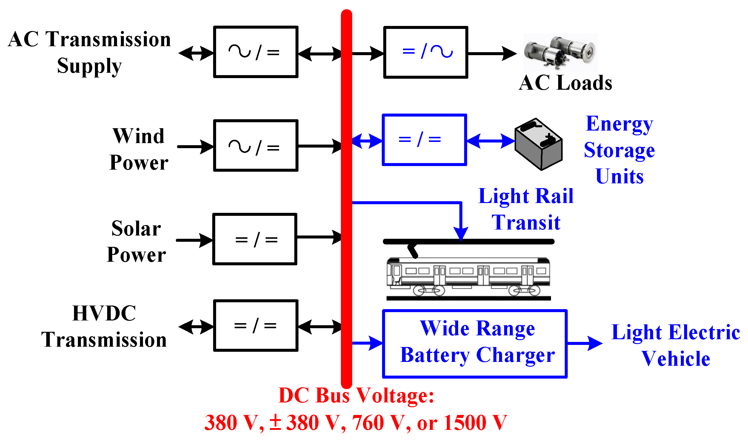
Figure 2.
Circuit configuration of (a) presented DC/DC converter at (b) low voltage output and (c) high voltage output.
Figure 2.
Circuit configuration of (a) presented DC/DC converter at (b) low voltage output and (c) high voltage output.


Figure 3.
Main PWM signals and circuit waveforms of the presented converter for (a) the low output voltage range and (b) the high output voltage range.
Figure 3.
Main PWM signals and circuit waveforms of the presented converter for (a) the low output voltage range and (b) the high output voltage range.
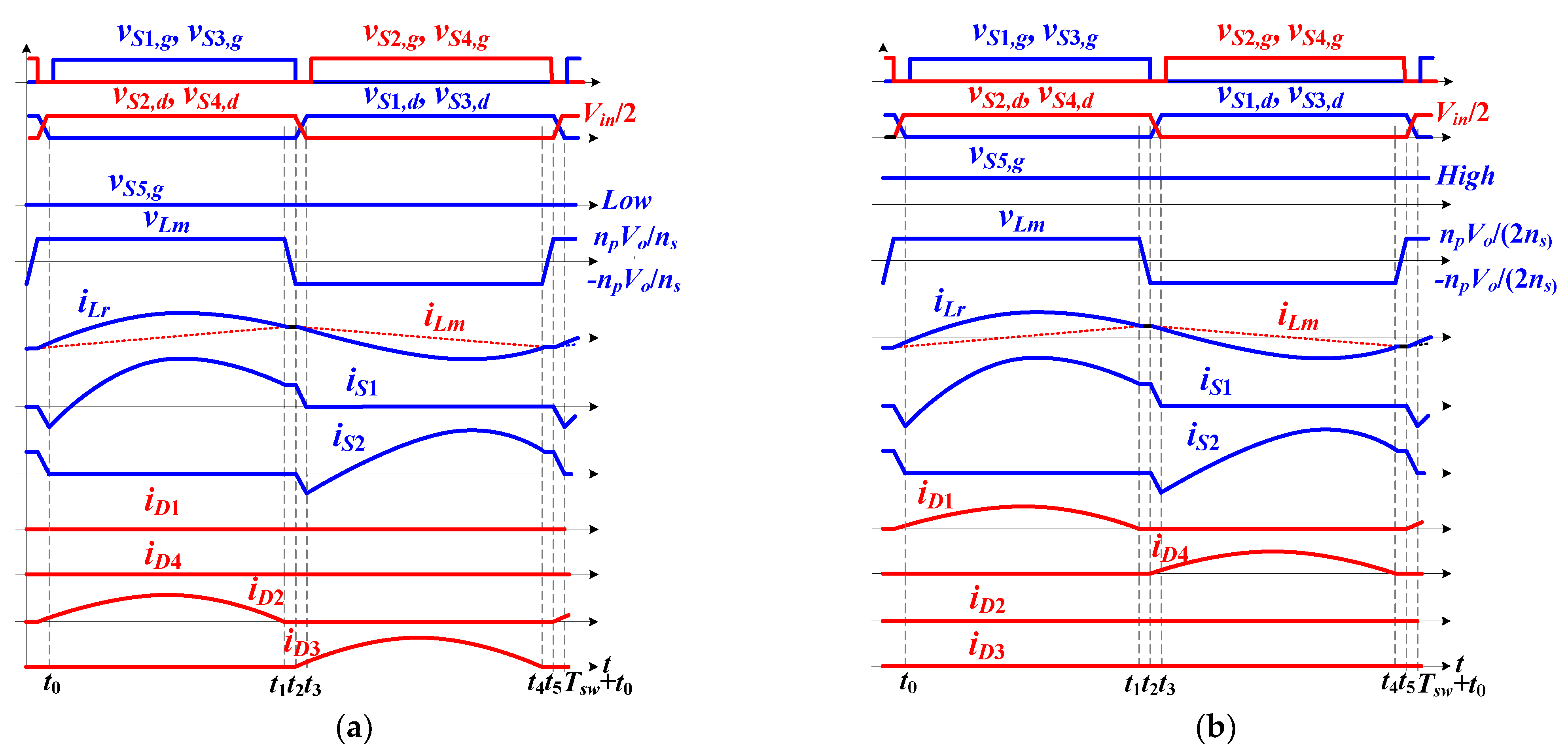
Figure 4.
Equivalent mode circuits under low voltage range operation if fsw < fr: (a) mode 1 circuit, (b) mode 2 circuit, (c) mode 3 circuit, (d) mode 4 circuit, (e) mode 5 circuit, and (f) mode 6 circuit.
Figure 4.
Equivalent mode circuits under low voltage range operation if fsw < fr: (a) mode 1 circuit, (b) mode 2 circuit, (c) mode 3 circuit, (d) mode 4 circuit, (e) mode 5 circuit, and (f) mode 6 circuit.

Figure 5.
Equivalent mode circuits under high voltage range operation if fsw < fr: (a) mode 1 circuit, (b) mode 2 circuit, (c) mode 3 circuit, (d) mode 4 circuit, (e) mode 5 circuit, and (f) mode 6 circuit.
Figure 5.
Equivalent mode circuits under high voltage range operation if fsw < fr: (a) mode 1 circuit, (b) mode 2 circuit, (c) mode 3 circuit, (d) mode 4 circuit, (e) mode 5 circuit, and (f) mode 6 circuit.
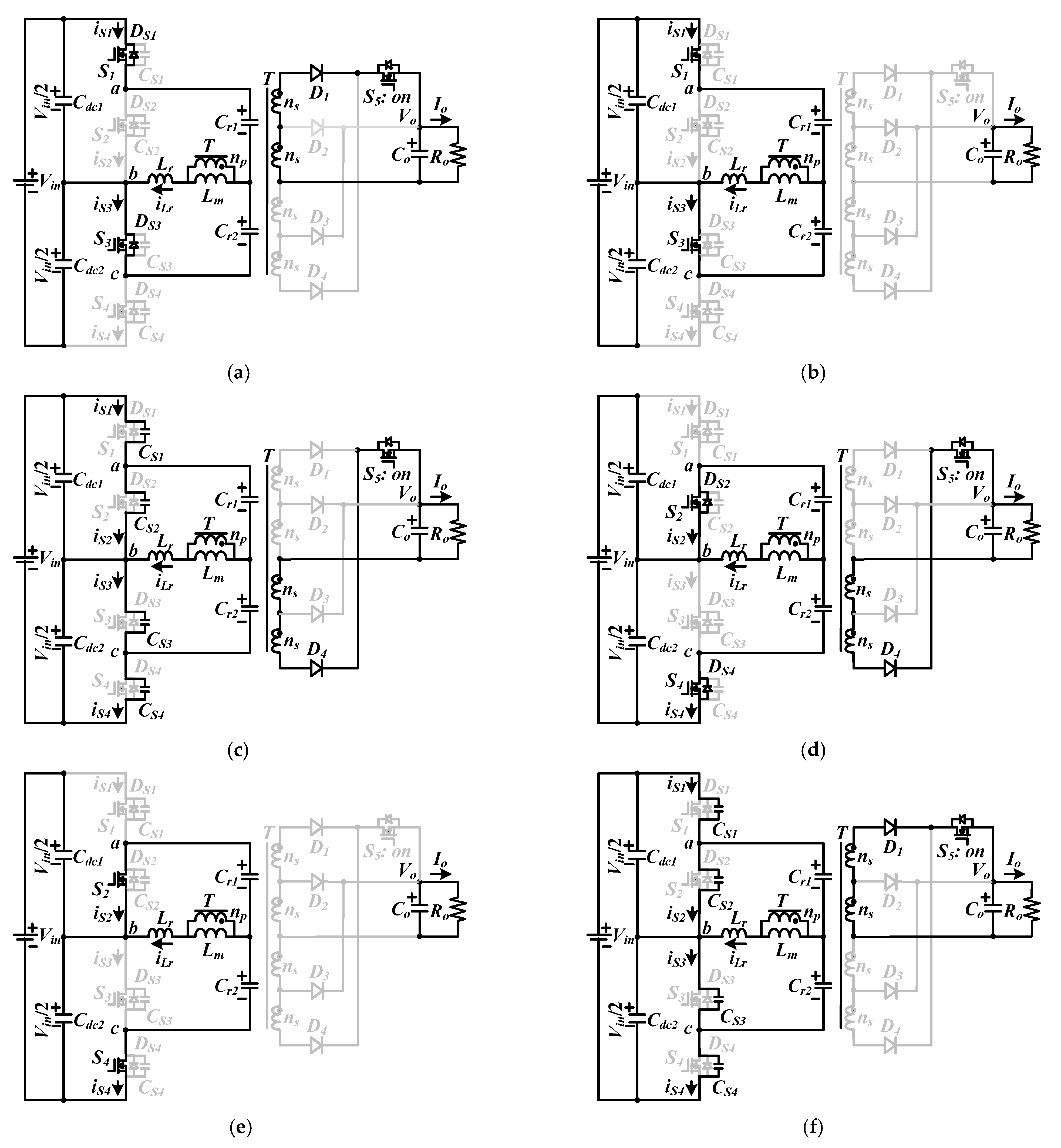
Figure 6.
Resonant Tank of the proposed converter: (a) equivalent AC circuit and (b) AC voltage gain.
Figure 6.
Resonant Tank of the proposed converter: (a) equivalent AC circuit and (b) AC voltage gain.

Figure 7.
Picture of the prototype circuit in the laboratory test.
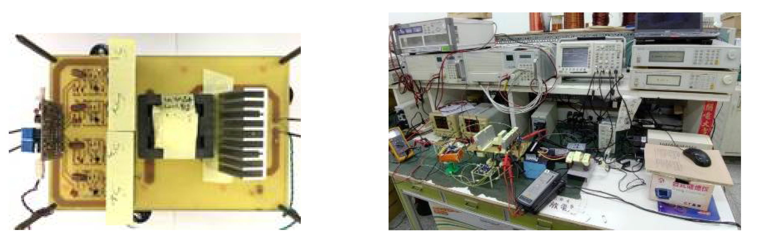
Figure 8.
Experiments of the presented converter under Vo = 50 V: (a) vS1,g, vS2,g, vS3,g, and vS4,g under Vin = 760 V and Po = 1 kW; (b) vS1,g, vab, and vbc under Vin = 760 V and Po = 1 kW; (c) vCr1, vCr2, and iLr under Vin = 760 V and Po = 1 kW; (d) iD2, iD3, Vo, and Io under Vin = 760 V and Po = 1 kW; (e) vS1,g, vS1,d, and iS1 under Vin = 760 V and Po = 200 W; and (f) vS1,g, vS1,d, and iS1 under Vin = 760 V and Po = 1 kW.

Figure 9.
Experiments of the presented converter under Vo = 90 V: (a) vS1,g, vS2,g, vS3,g, and vS4,g under Vin = 760 V and Po = 1 kW; (b) vS1,g, vab, and vbc under Vin = 760 V and Po = 1 kW; (c) vCr1, vCr2, and iLr under Vin = 760 V and Po = 1 kW; (d) iD2, iD3, Vo, and Io under Vin = 760 V and Po = 1 kW; (e) vS1,g, vS1,d, and iS1 under Vin = 760 V and Po = 200 W; and (f) vS1,g, vS1,d, and iS1 under Vin = 760 V and Po = 1 kW.
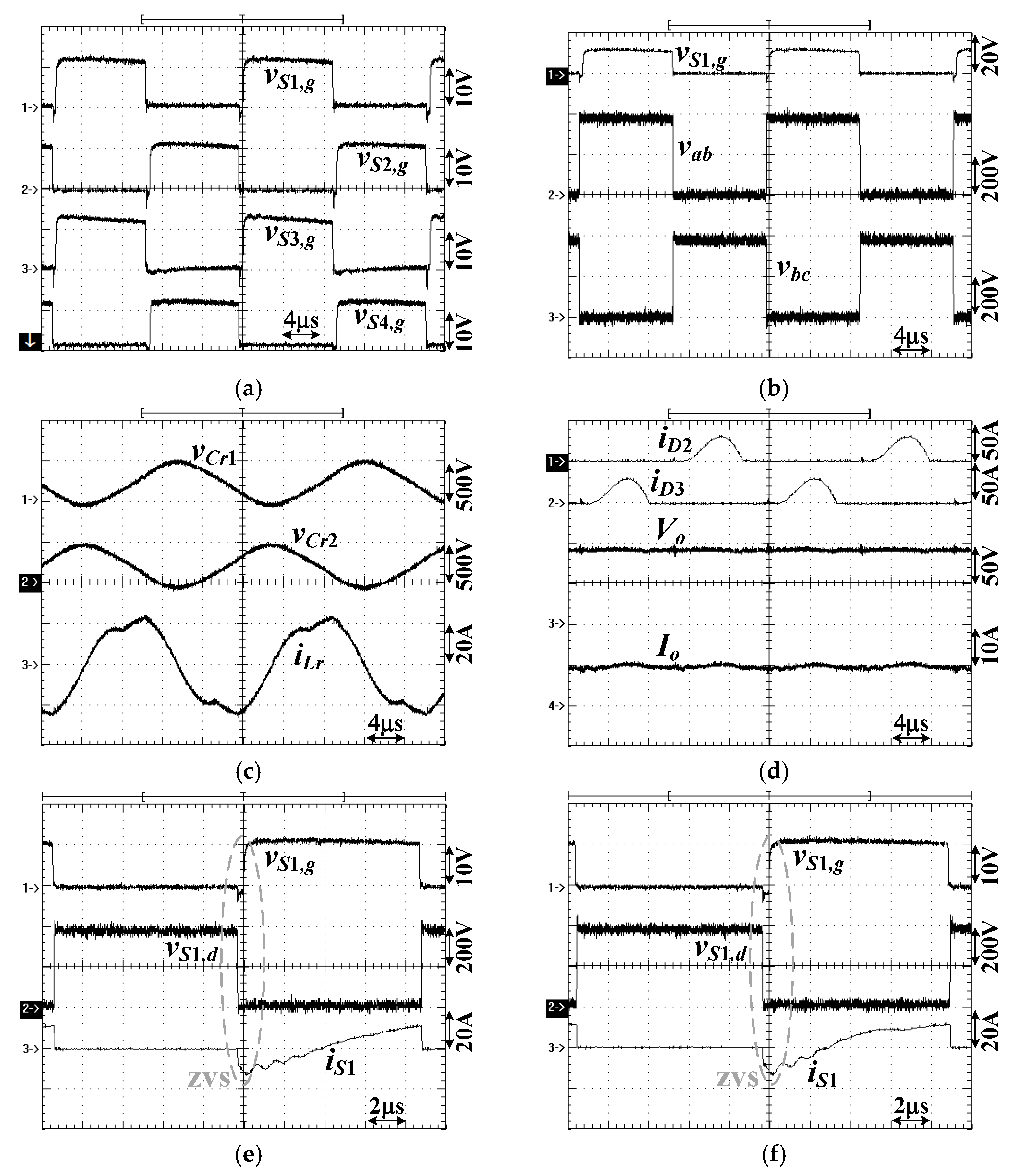
Figure 10.
Experiments of the presented converter under Vo = 95 V: (a) vS1,g, vS2,g, vS3,g, and vS4,g under Vin = 760 V and Po = 1 kW; (b) vS1,g, vab, and vbc under Vin = 760 V and Po = 1 kW; (c) vCr1, vCr2, and iLr under Vin = 760 V and Po = 1 kW; (d) Io, Vo, iD1, and iD4 under Vin = 760 V and Po = 1 kW; (e) vS1,g, vS1,d, and iS1 under Vin = 760 V and Po = 200 W; and (f) vS1,g, vS1,d, and iS1 under Vin = 760 V and Po = 1 kW.
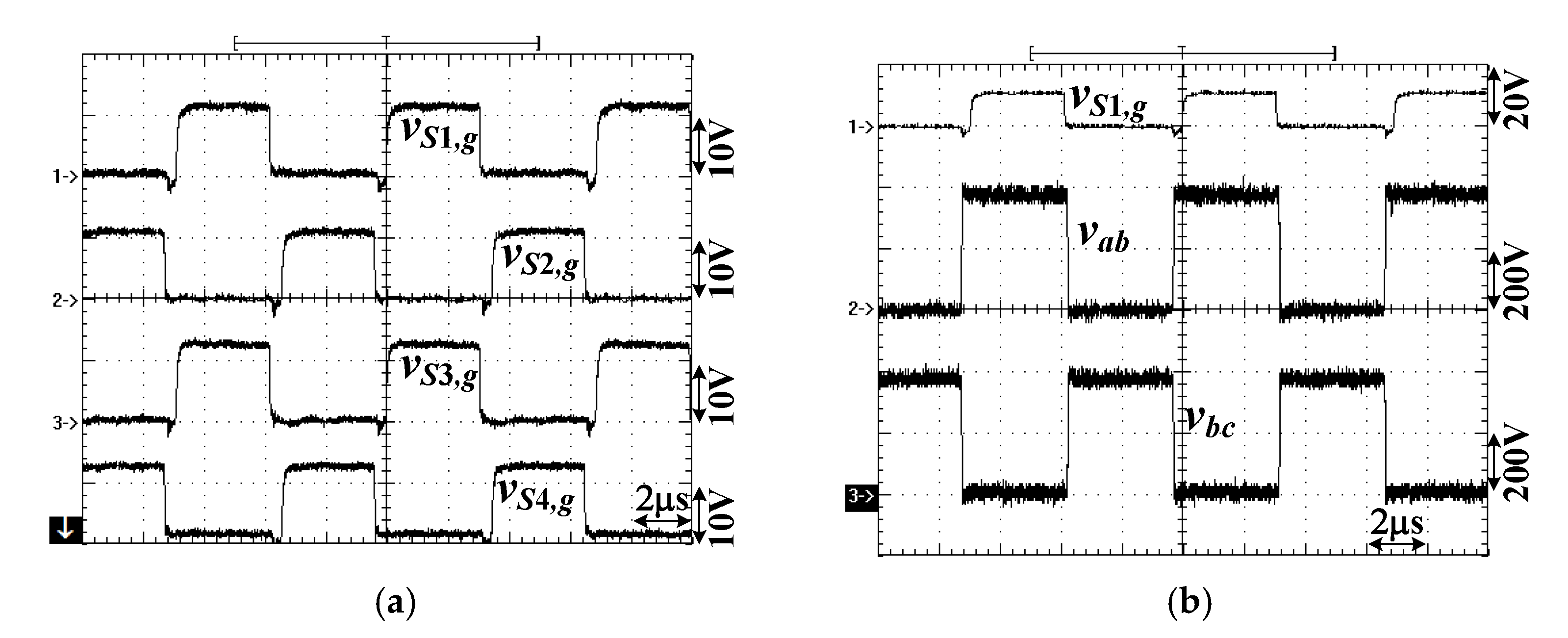
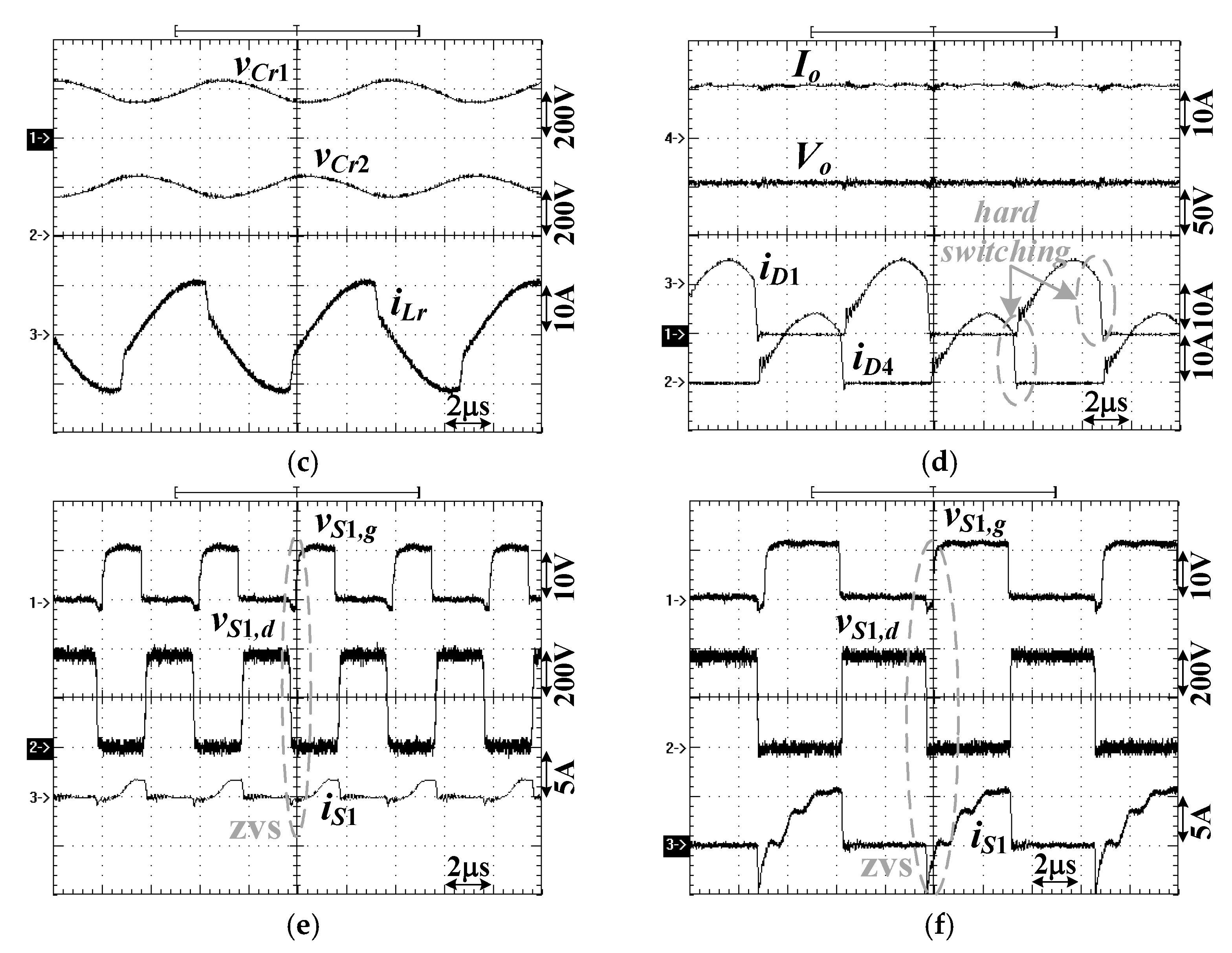
Figure 11.
Experiments of the presented converter under Vo = 160 V: (a) vS1,g, vS2,g, vS3,g, and vS4,g under Vin = 760 V and Po = 1 kW; (b) vS1,g, vab, and vbc under Vin = 760 V and Po = 1 kW; (c) vCr1, vCr2, and iLr under Vin = 760 V and Po = 1 kW; (d) Io, Vo, iD1, and iD4 under Vin = 760 V and Po = 1 kW; (e) vS1,g, vS1,d, and iS1 under Vin = 760 V and Po = 200 W; and (f) vS1,g, vS1,d, and iS1 under Vin = 760 V and Po = 1 kW.
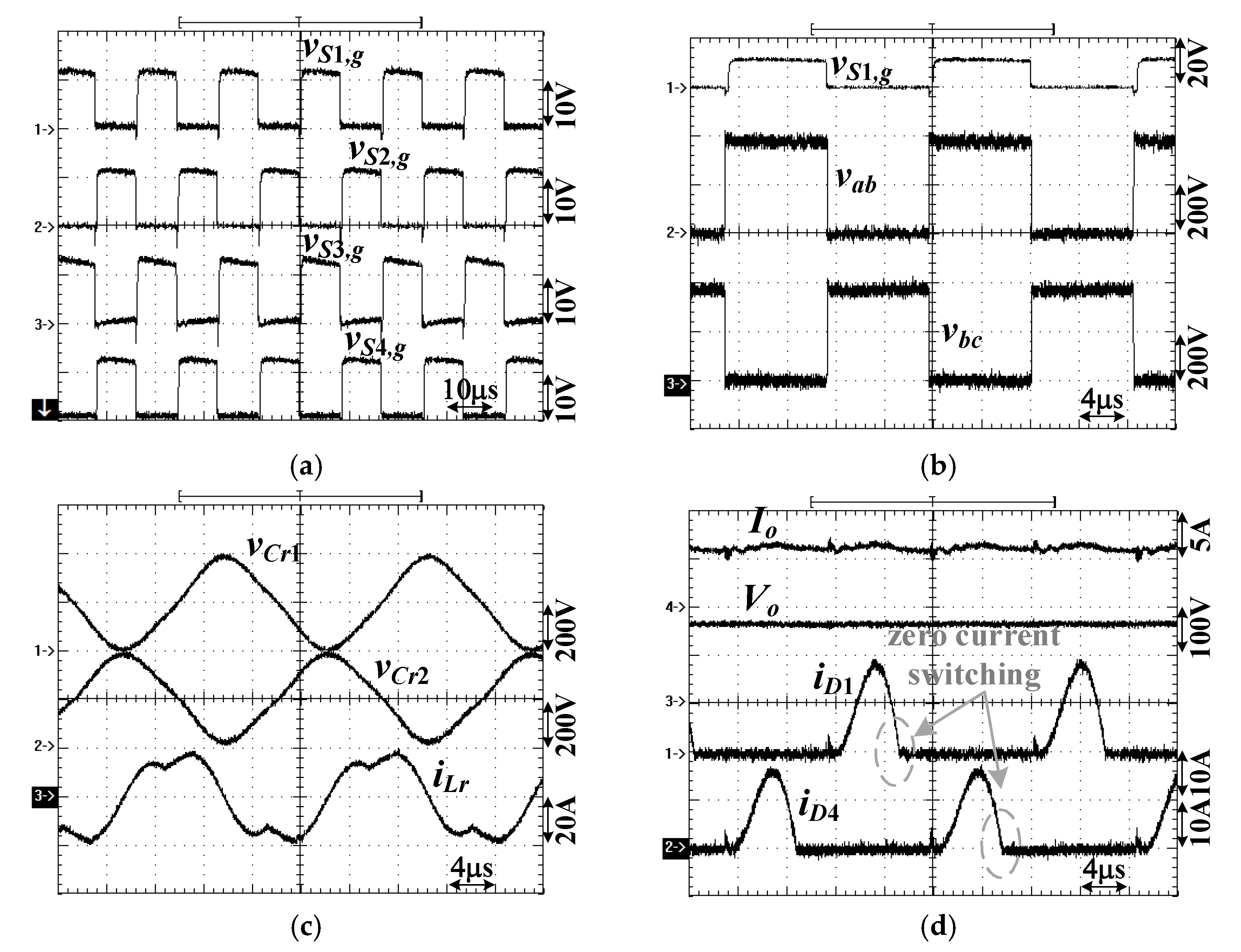

Figure 12.
Experiments of Vo and Io during output voltage variation between 50 and 160 V.


Table 1.
Circuit components in the prototype circuit.
| Items. | Parameter | Items | Parameter |
|---|---|---|---|
| Vin | 760 V | Vo | 50~160 V |
| Po | 1 kW | S1~S4 | STF40N60M2 (650 V/22 A) |
| Cin1, Cin2 | 330 µF/450 V | D1~D4 | STTH15R06D (600 V/12 A) |
| fr,1 | 100 kHz | S5 | 6R070P6 (650 V/33 A) |
| Co | 1360 µF/200 V | np:ns | 32:8 |
| Lr | 8.35 µH | Lm | 62.6 µH |
| Cr1, Cr2 | 152 nF |
Publisher’s Note: MDPI stays neutral with regard to jurisdictional claims in published maps and institutional affiliations. |
© 2021 by the author. Licensee MDPI, Basel, Switzerland. This article is an open access article distributed under the terms and conditions of the Creative Commons Attribution (CC BY) license (https://creativecommons.org/licenses/by/4.0/).
Share and Cite
MDPI and ACS Style
Lin, B.-R. Analysis and Implementation of a Frequency Control DC–DC Converter for Light Electric Vehicle Applications. Electronics 2021, 10, 1623. https://doi.org/10.3390/electronics10141623
AMA Style
Lin B-R. Analysis and Implementation of a Frequency Control DC–DC Converter for Light Electric Vehicle Applications. Electronics. 2021; 10(14):1623. https://doi.org/10.3390/electronics10141623
Chicago/Turabian StyleLin, Bor-Ren. 2021. "Analysis and Implementation of a Frequency Control DC–DC Converter for Light Electric Vehicle Applications" Electronics 10, no. 14: 1623. https://doi.org/10.3390/electronics10141623
Note that from the first issue of 2016, this journal uses article numbers instead of page numbers. See further details here.