Article

Modeling of PV Module and DC/DC Converter Assembly for the Analysis of Induced Transient Response Due to Nearby Lightning Strike

by
Alessandro Formisano
1,
Jesus C. Hernández
2,*,
Carlo Petrarca
3 and
Francisco Sanchez-Sutil
2
1
Department of Engineering, University Della Campania “Luigi Vanvitelli”, Via Roma 29, 81031 Aversa, Italy
2
Department of Electrical Engineering, Campus Lagunillas s/n, University of Jaén, Edificio A3, 23071 Jaén, Spain
3
Department of Electrical Engineering and Information Technology, University di Napoli “Federico II”, Via Claudio 21, 80125 Napoli, Italy
*
Author to whom correspondence should be addressed.
Electronics 2021, 10(2), 120; https://doi.org/10.3390/electronics10020120
Submission received: 16 December 2020 / Revised: 30 December 2020 / Accepted: 4 January 2021 / Published: 8 January 2021

Abstract

:
Photovoltaic (PV) systems are subject to nearby lightning strikes that can contribute to extremely high induced overvoltage transients. Recently, the authors introduced a 3D semi-analytical method to study the electromagnetic transients caused by these strikes in a PV module. In the present paper we develop an improved model of the PV module that: (a) takes into account high-frequency effects by modelling capacitive and inductive couplings; (b) considers the electrical insulation characteristics of the module; (c) includes the connection to a DC/DC converter. The whole process involves three major steps, i.e., the magnetic-field computation, the evaluation of both common-mode- and differential-mode-induced voltages across the PV module, and the use of the calculated voltages as input to a lumped equivalent circuit of the PV module connected to the DC/DC converter. In such a framework, the influence of the PV operating condition on the resulting electrical stresses is assessed; moreover, the relevance or insignificance of some parameters, such as the module insulation or the frame material, is demonstrated. Finally, results show that the induced overvoltage are highly dependent both on the grounding of the conducting parts and on the external conditions such as lightning current waveforms and lightning channel (LC) geometry.

1. Introduction

The increasing generation of electric power from PV sources requires larger PV modules size, which get more exposed to open-field weather conditions, and consequently can be more susceptible to direct or indirect lightning discharges [1,2,3,4]. Assemblies of PV modules, called PV arrays, are usually equipped with lightning protection systems to avoid damages due to direct lightning [5]. However, the more likely event of a strike hitting nearby the PV array can still cause relevant effects and possibly damage the PV modules [2,6,7,8] or other PV components [9,10,11]. The study of lightning effects on PV modules is therefore a key issue for their safety [4]. Particularly, the knowledge of lightning-induced voltage on a PV module and its characteristics [1] gives the engineer an opportunity to take specific measure for its protection in the PV system design phase.
Active research on the lightning effects on PV systems [12] recently showed a massive increase. In [2], scientific background and essential assumptions taken for the design of lightning protection systems for PV systems are discussed. Field measurements are presented in [6,13,14], and the performance of PV systems under both direct and indirect lightning strikes is investigated. Experimental tests on single PV modules or reduced-scale PV arrays are analyzed in [3,8,15,16,17,18,19,20,21,22] to show the transient behavior. Overvoltage at the DC side is addressed in [3,4,8,14,15,16,17,18,19,20,21,22,23,24,25,26,27,28,29]. Recently, the degradation of the PV module under impulse voltage was investigated [7,30,31,32,33,34].
Note that previous simulation studies focused on single PV modules [15,16,19,20,21,22] or reduced-scale PV arrays [3,6,15,18,22,23,25,28,29] are mainly based on over-simplified models. They cannot provide a complete and systematic evaluation of the lightning-induced overvoltage. For example, the inductive coupling between the inner wiring structure of the PV module and its metal frame is almost always omitted due to its computational complexity [1,15,16,21,22]. Additionally, the capacitive coupling among metallic parts inside and around the PV module is never considered (see, e.g., [19,35,36,37]). Consequently, the induced transient voltages resulting from the presence of both coupling mechanisms have not been accurately assessed to date.
Modelling and value setting of dynamic AC circuit parameters for a PV module gives important insight to characterize and diagnose its behavior in case of lightning events. Extensive studies on the determination of parameters of the active electrical circuitry for PV cells and modules are available in the literature, mostly focused on calculating both the DC and AC electrical parameters [38,39,40,41,42,43,44,45,46,47,48,49,50,51,52,53]. The most widely used method to study the PV dynamic behavior is the impedance spectroscopy [40,43,54,55,56,57,58]. Alternative methods are based on time domain techniques [59,60]. Based on these or other methods, the AC parameters of a PV cell/module, such as capacitance and parallel and series resistance, can be accurately characterized. However, there are few studies on the characterization of parameters related to the PV module electrical insulation [23,36,61,62].
Although efforts have been made to characterize the high-frequency modelling of PV module/array under lightning strikes, as previously described, it is found that studies usually considered simple frequency models for the PV array components (inaccurate models under transient conditions), and just a few researchers have considered accurate high-frequency models [13,23]. An efficient high-frequency modelling for the PV module would therefore be necessary to provide effective lightning protection. In this context, the authors proposed in [1] a 3D semi-analytical method, able to predict the transient overvoltage induced in a PV module by an indirect lightning, considering both capacitive and inductive coupling effects.
The present paper shows results extending the previous work [1] while adding two important contributions. The first one is the proposal of an improved modelling for the PV module, able to cope also with high-frequency effects and to treat the module insulation to frame and to ground, also including the connection to a DC/DC converter. This allows to analyze the influence of different PV operating conditions (module voltage bias) on lightning induced voltages. The assumed parameter variations are based on an exhaustive literature review [38,39,40,41,42,43,44,45,46,47,48,49,50,51,52,53,54,55,56,57,58,59,60,61,62,63].
The second contribution involves a comprehensive sensitivity analysis that conclusively demonstrates the relevance (or the insignificance) of certain parameters, such as the module insulation (dependent on meteorological conditions) or the frame material. Additionally, these overvoltages were found to be highly dependent on factors external to the DC/DC converter-PV module assembly, such as the lightning current waveform or the lightning channel geometry.
The rest of the paper is structured as follows. The mathematical model for computing the magnetic field from a lightning channel is briefly recalled in Section 2. The description of the PV module is detailed in Section 3. The LC–module coupling as well as the detailed model for the PV module and DC/DC converter are presented in Section 4. Our comprehensive analysis of the influence on inducted voltages of the PV operating conditions and value setting for some parameters of the PV module model as well as other relevant external aspects of this phenomenon is presented in Section 5. Concluding remarks are noted in Section 6.

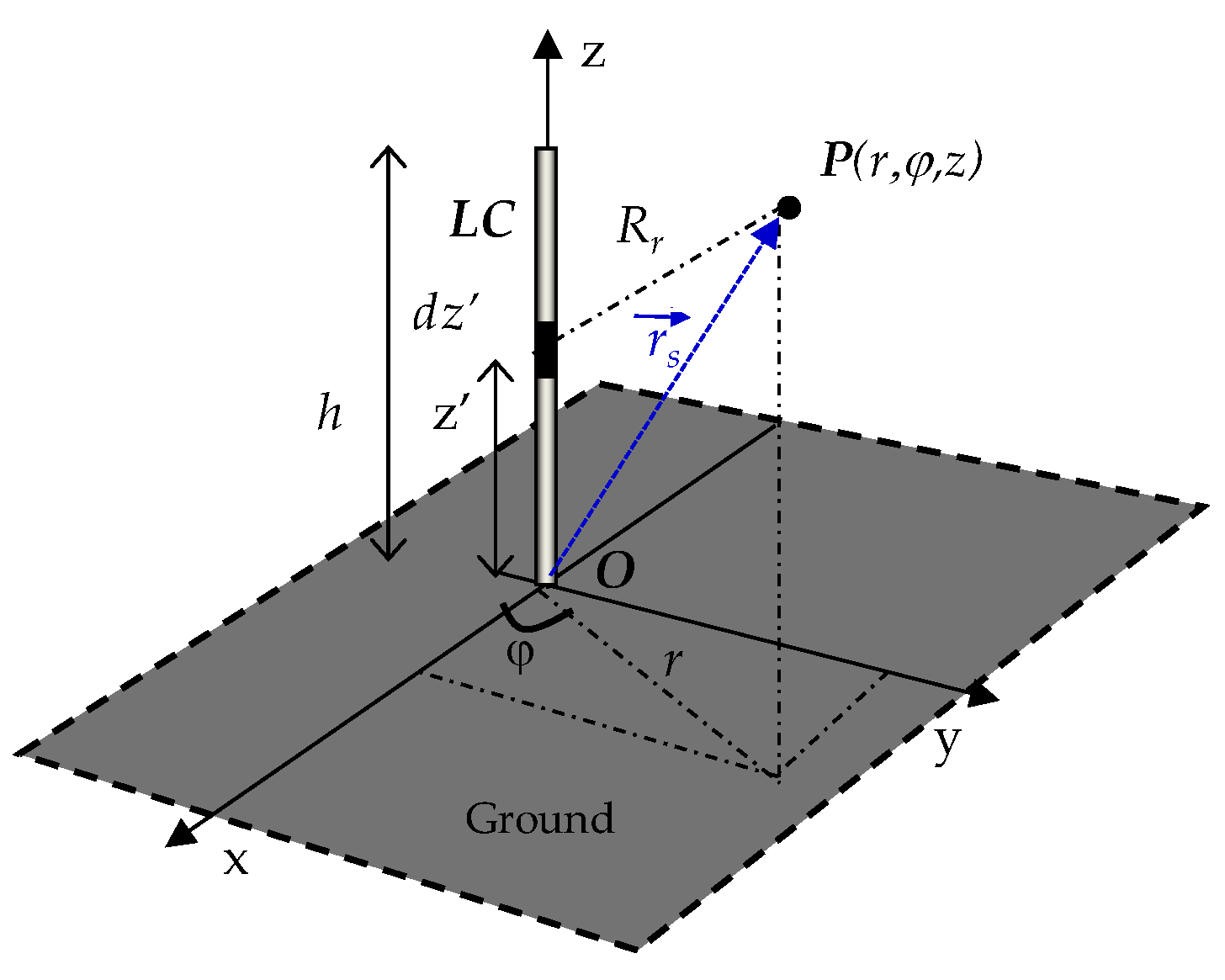
2. Magnetic-Field Computation from a Lightning Channel

This section summarizes the magnetic field computation from a tortuous LC developed by the authors (see [1,64,65] for a more detailed description). The LC is represented by a number of arbitrarily oriented segments Ck; it starts from an infinitely conducting ground in proximity of a PV module and develops towards the clouds (Figure 1). Parameters describing the channel geometry are chosen according to data about natural flashes presented in [66]: the average absolute value of the angle between adjacent segments φ is assumed to be equal to 17° in this study (both positive and negative values are allowed). The average length of each segment is L m = 8.5   m . The overall length of the channel is L = 10   km . The LC is travelled by a lightning current of amplitude I 0 that propagates without attenuation or distortion at constant speed v , equal to 1/3 of speed of light c in vacuum.
In case of a vertical lightning channel (Figure 2) starting from ground, the magnetic vector potential A ( r ¯ s , t ) from the LC is given by
A ( r ¯ s , t ) = μ 0 4 π 0 h I 0 ( t ) u ( t R r c z v ) R r d z i ^ z
where h is the channel height, u is the Heaviside step function, μ 0 is the vacuum permeability and the main geometrical parameters are represented in Figure 2. The method of images is then adopted to take into account the presence of the perfectly conductive ground: an “image channel” is located under the ground plane and is travelled by the same current and carries an opposite charge. The vector potential A ( r ¯ s , t ) is finally line-integrated along the inner circuitry of each module and along the boundaries of the aluminum protection case, and time-differentiated to evaluate both common-mode- and differential-mode-induced overvoltage. Full details about Equation (1) and the underlying model are given in [1,65].
In the case of a tortuous LC, it is necessary to calculate and then sum up the contributions of each segment Ck composing the lightning path. Such a contribution can be easily calculated by using the same Formula (1) if a suitable local cylindrical coordinate system is adopted, as shown in Figure 3.
Regarding the lightning current waveform I 0 ( t ) at ground, the typical analytical expressions as reported in the IEC standards [67] has been adopted
I 0 ( t ) = I p e a k η ( t τ 1 ) n 1 + ( t τ 1 ) n e x p ( t τ 2 )
Full details about the current waveform model are reported in the IEC Standard. Assuming that the current propagates undistorted along the channel, the computation of the vector potential produced by a generic current I 0 ( t ) starting from the ground can then be performed by the Duhamel’s theorem and by the convolution product with the vector potential calculated at the same point and generated by a unit step current.
The waveforms adopted in this study are typical of either a first negative short stroke (Figure 4a) or a subsequent negative short stroke (Figure 4b); the related parameters are reported in Table 1.

3. Modeling of the PV Module

3.1. Wiring of the PV Module

The PV module is a packaged, connected assembly of PV cells with a metal frame. PV cells within a PV module are series connected to achieve higher voltage output, as the voltage produced by a single cell is limited. Figure 5a shows the dimensions of the investigated PV module. The standard PV module has 270-watt output power from a matrix of 60 square cells, with a size of 156 mm, series connected to reach a maximum output voltage of 114.18 V. The cells are sealed in the module to protect from the environment, and DC cabling is provided to connect cells in series.
According to the actual size of the PV module and its spatial distribution, the PV inner wiring complex 3D shape is modelled by connections with a thin-wire structure and developing on a planar path Figure 5b). Since the up–down transitions on different planes of the semiconductor cells do not contribute significantly to the concatenated magnetic flux and, consequently, to induced voltages [1], we assumed a planar path for the cell interconnections; consequently, the connections create a geometric loop (see the equivalent brown line Γ in Figure 5b,c), determining a differential-mode area Adm (grey). The conducting frame around the PV module determines a second closed loop, enclosing the frame area Af (green). The relative complement of the internal loop area Adm and the frame loop area Af determines the common-mode area Acm (purple). Therefore, the 3D model (Figure 5d) incorporates features such as the geometries of the frame and the traces which connect the PV cells within the module.
The model of the PV module assumes a 1 m height and a 35° tilt with respect to the ground, with the LC touching ground 5 m away from the lower left corner of the module. The ground is aligned to the xy plane, and the LC develops along the z axis on the average. With the assumption that it would have a negligible effect on the simulation results, the glass sheet at the front of a PV module is omitted.

3.2. PV Metallic Frame

Traditional PV modules are commonly embedded in a metal frame. The frame can help to fix and seal the PV module and protect the module from damages during transportation and installation. For the sake of information, we note that frameless modules also have advantages, as they reduce the possibility of electric shock and of potential-induced degradation [36,68].
The frame equivalent resistance is computed by assuming an even current density distribution and adopting the standard expression
R f r a = ρ · l fra / S C
where ρ is the material resistivity (aluminum and steel data are discussed in Section 5), l f r a is the total length of the four frame sides, and S C is the C shape equivalent section.
The frame equivalent self-inductance Lfra is computed by modeling the frame as a rectangular coil, with a square section [69], with dimensions fitting the equivalent area of the C-shaped actual section, and adopting suited shape coefficients to compensate for the different current density distribution. Internal inductance is neglected. Mutual inductance with the PV circuitry Mfra-mod is computed using the code INDIANA [69], developed by the authors, based on the line integration of vector potential.
Thanks to its excellent mechanical performance (high strength, lightweight, easy installation), a C-shaped steel or aluminum profile is commonly used in PV modules. The profile used in this paper has a higher width of 40 mm and the thickness of 3 mm. Note that, while aluminum can be assumed nonmagnetic, steel may show nonlinear magnetic behavior. We neglected this aspect in the study, assuming a nonmagnetic steel [70]. We also neglected frequency-dependent current redistribution.

4. Modelling of the PV Module and DC/DC Converter Assembly

4.1. Modelling for the PV Module

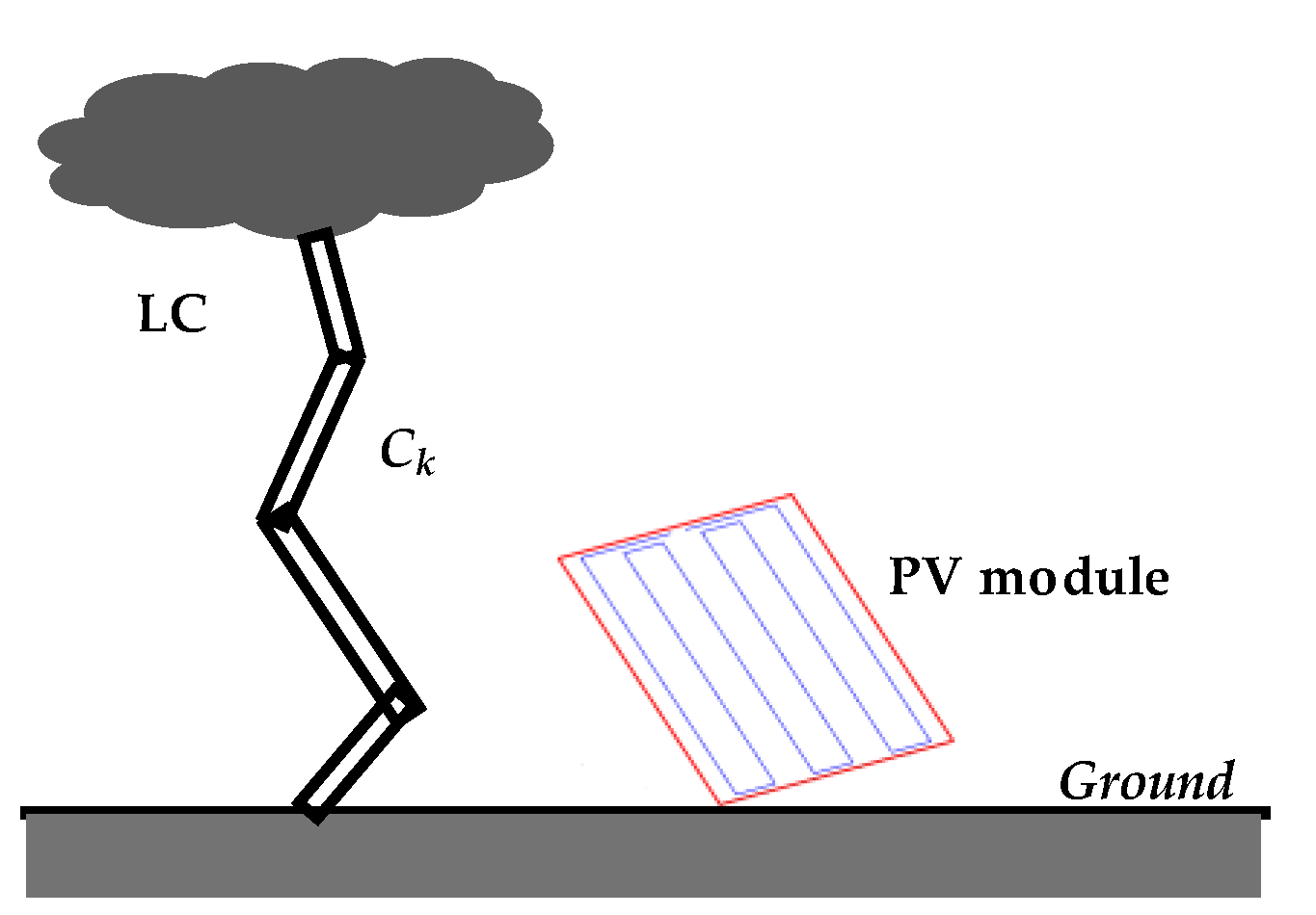
4.1.1. Lightning Channel Coupling Model for a Single PV Module

Since this study only accounts nearby lightning strikes, not directly hitting the PV power system, only the induction effects due to lightning current must be considered. Taking into account the lightning current magnitude, and the relatively limited dimensions of the PV module, a straightforward computation demonstrates that the relevant coupling mechanism in this case is the inductive coupling, as reported in [1,16].
The coupling between the LC and the module (see Figure 6) is modelled by introducing two equivalent voltage sources: an equivalent voltage source (Vmod) simulating the coupling of the LC with the module inner electrical circuitry (area Adm, Figure 5c) and another voltage source (Vfra) that gathers the coupling with the conducting frame (area Af, Figure 5c).

4.1.2. Dynamic and Insulation Model of a PV Module

The models of active electrical circuitry for PV cells were extensively studied over the years. The single-diode model [71], double-diode model, and modified three-diode equivalent circuit model [72], are the most adopted ones to represent the PV cells in circuit simulation under DC conditions. For the lightning transient study in this paper, the dynamic PV single-diode model is adopted, as shown in Figure 7a. Ig is the photocurrent. For the dynamic analysis considered here, the equivalent PV cell electric circuit is obtained by replacing the diode with the diffusion capacitance (CD,PVc), the transition capacitance (CT,PVc) and the dynamic resistance of diode (Rd,PVc), Figure 7b [38,39]. The transition capacitance describes the charge stored in the depletion region at the semiconductor p-n junction and the diffusion capacitance describes the charge stored in the neutral region of the semiconductor outside the depletion region [40,41]. The magnitude of diffusion capacitance is much larger than the transition capacitance one. It happens to be prominent when the p-n junction is forward-biased and negligible when reverse-biased. Transition capacitance dominates at small positive and negative voltages, where the junction is not conducting a significant current, and diffusion capacitance dominates above the voltage of the MPP, where the junction carries a significant current.
The current source is ignored due to its value, which is much lower than the lightning-induced current. Series resistance (Rs,PVc) results from the bulk resistance of the p- and n-layers to majority carriers flow as well as from the Ohmic contacts on the cell to the external wiring. Shunt resistance (Rsh,PVc) results primarily from the leakage currents around the edges of the PV cell, but also from the low insulation at both terminals of the PV cell. This parameter shows a high uncertainty, due to inhomogeneities and defects resulting from the production process.
The series resistance (Rs) and the series inductance (Ls) model the parasitic effects associated with cables and connectors and are assumed to be constant.
The dynamic model can be simplified using a parallel resistance (Rp,PVc) which is the result of combining Rd,PVc with Rsh,PVc and a parallel capacitance Cp,PVc, which is the result of combining CD,PVc with CT,PVc; see Figure 7c.
When PV cells are arranged in series and parallel in a PV module, the dynamic parameter values of the module are the combination of the individual cell characteristics. The dynamic impedance of the PV module in dark conditions at the working frequency ω can be calculated using the following equation
Z P V m = [ R s , P V m + R p , P V m ( ω R p , P V m C p , P V m ) 2 + 1 ] j [ ω R p , P V m 2 R p , P V m ( ω R p , P V m C p , P V m ) 2 + 1 ]
Details of the derivation can be found in [49] or [61]. The parameter values of the PV cell/module model are not constant, but depend on irradiation, temperature, and cell/module voltage bias [40,43,54,59]. Generally, increasing voltage bias increases parallel capacitance and decreases parallel resistance [40,42,54]. As temperature increases, resistance decreases due to a higher number of free carriers and capacitance increases. Similarly, increasing irradiation lowers parallel resistance and increases parallel capacitance [40,56].
Regarding series resistance, this is voltage independent and only is influenced by irradiance [44] and temperature [23]. As an example, its value decreased up to three times when irradiance increased from 100 to 1200 W/m2.
Regarding parallel resistance, dynamic resistance (Rd,PVc) is voltage-dependent and shunt resistance (Rsh,PVc) is voltage-independent [43,45]. Furthermore, parallel resistance achieves the highest values at dark conditions, about 7 to 22 times to that of the full irradiation [42,46,47]. Focusing on low irradiation conditions, parallel resistance decreases as positive voltage bias increases. Thus, reference [42] reported that this resistance at MPP and Open-Circuit (OC) conditions could achieve a 3.03% and 0.17% value, respectively, compared to that of the Short-Circuit (SC) condition. Nonetheless, a lower change of about three times between MPP and OC conditions was reported in [44,48].
Regarding parallel capacitance, transition capacitance (CT,PVc) is voltage-dependent whereas diffusion capacitance (CD,PVc) is voltage- and frequency-dependent [43,45,46,50,59]. Therefore, the mathematical model of parallel capacitance (Cp,PVc) at various frequency f and voltage bias of the PV cell VPVc is identified by curve fitting using [49]
C p , P V c ( V P V c , f ) = a ( 1 V P V c b ) 1 / 2 + [ c 2 π f e x p ( V P V c d ) ] ( 1 + e ( 2 π f ) 2 1 ) 1 2
where a, b, c, d are fitting parameters. Details on the extraction of these parameters can be found in [73].
Focusing on low irradiation conditions (about 100 W/m2), reference [42] describes that the parallel capacitance at MPP and OC conditions could achieve a 294% and 340% value, respectively, compared to that of the SC condition. The resulting parallel capacitance is also irradiance-dependent [42,46,51,59,60]. Thus, for different voltage biases, this capacitance could decrease in the range 15% to 70% when irradiance decreases from high to low irradiation [42,60].
Self-inductance (Ls) and wiring resistance (Rs) were computed using the approach described above. It was found in the literature [3] that both the resistance (Rs) and inductance (Ls) were almost frequency-invariant and were coincident with the DC inductance and DC resistance, respectively.
This section concludes with modeling the PV module electrical insulation (insulation resistance and capacitance). This variable is key for human safety and the reliability of a PV module [36,68]. The equivalent circuit model that emulates the behavior of the PV module insulation was already defined in [36], Figure 8. Thus, the model consists of a leakage capacitance (Cp,iso,PVm), a series insulation resistance (Rs,iso,PVm), and a parallel insulation resistance (Rp,iso,PVm).
The insulation parameter values change with meteorological conditions, namely, the relative humidity and the module temperature [36]. High values of relative humidity and module temperature were the meteorological variables that determined the lowest module insulation resistance Riso,PVm (Rs,iso,PVm + Rp,iso,PVm) and the highest leakage capacitance. This usually happens at sunrise on winter days. The opposite insulation condition, i.e., the highest insulation resistance and the lowest leakage capacitance, typically occurs in summertime.
Because of the change in meteorological conditions, module leakage capacitance can increase from the lowest values up to 65 times, whereas the series and parallel insulation resistances can decrease from the highest values up to 9.2 and 46 times, respectively [69].
The values adopted for the parameters described in this section are introduced in Section 5, both for a reference case and for a number of parametric studies, to help assess the sensitivity of induced overvoltage to the most relevant parameters.

4.2. Modelling of the DC/DC Boost Converter

The boost converter for the DC load connection from the PV module consists of an insulated-gate bipolar transistor (IGBT)-diode pair switch, an LC filter (Lboost and Cboost) and a control circuit, Figure 9. The employed DC/DC power converter increases the DC MPP voltage of the PV module and converts an unregulated input voltage (i.e., distorted 114.18 V) to a regulated output voltage of 120 V. Several power converters provide a fixed output reference to ensure that the delivered output voltage is always set on a specific value regardless of the input [62,74,75]. More specifically, the high-frequency model of DC/DC converter is as follows: at the DC load side, two parameters, Rdc,w and Ldc,w, were added to represent the parasitic resistance and inductance of the connecting wires on the converter’s DC side. Similarly, at the PV module side, Rpv,w and Lpv,w were added to represent the connections to the PV module. A resistance RLoad was added to represent the load. Finally, the IGBT-diode pair switch was modelled by an ideal switch in series with an R branch formed of a resistance Rsw,on in order to take the commutation losses into consideration. The commutation speed of the power device was reproduced by an R-C branch (Rsw,sh, Csw,sh) connected in parallel to the device.
As explained, the insulation model of the PV module includes a leakage capacitance and a series/parallel insulation resistance. The ground path impedance was indicated with Zgn. The electrical model of converter insulation includes both the stray shunt capacitance Csw,shunt and shunt resistance Rsw,shunt between the aluminum radiator of IGBT module and the ground.
The ground is assumed here as the common reference voltage. Therefore, the common mode voltage at the terminals of the DC/DC converter is as follows
V c m = V n e g . g n d + V p o s . g n d 2
The differential mode voltage is the input converter voltage
V d m = V p o s . g n d V n e g . g n d
The common mode current is the sum of the two-line input current
I c m = I 1 + I 2
and the differential mode current is given by
I d m = I 1 I 2 2
The differential mode current corresponds to the current injected into the converter, while the common mode current flows through the parasitic resistive/capacitive couplings between the different parts of the PV module and the ground connection. For this reason, it is known also as the ground current.
The converter inductance and capacitance are given by the basic rules for the design of a boost converter in continuous conduction mode
L b o o s t = V i n · D f s · Δ I L b o o s t
C b o o s t = I o u t · D f s · Δ V C b o o s t
where D is the duty cycle of the converter, fs is the switching frequency, and the other quantities are related to the voltage and current ripples.

5. Results

5.1. Simulation Setup

The whole mathematical model involves three major steps, i.e., the magnetic vector potential computation, the evaluation of consequent overvoltage at different loops of the PV module, and the computation of overvoltages in the lumped-equivalent circuit model of PV module and DC/DC converter.
The induced voltages due to coupling between lightning channel and PV module elements were computed using the self-developed computational electromagnetic package, as discussed in Section 2. These overvoltages were fed to a SPICE model and to a MATLAB/Simulink model, both using the lumped-equivalent circuit model for PV module and DC/DC boost converter described in Section 4. Circuitry simulations in both simulation environments allowed a cross validation of results.

5.2. Input Data

Unless otherwise stated, the parameter shown in Table 2 for the full circuitry model of the PV module and DC/DC converter assembly, Figure 10, were computed at a frequency of 1 MHz, which reflects the fundamental timescale of the simulated lightning current waveforms.
Dynamic impedance of the PV module was assessed under cloudy conditions, i.e., 100 W/m2, when there are storms and nearby lightning strikes can appear. Furthermore, different PV operating conditions (module voltage bias), from short-circuit to open-circuit conditions, influenced the evaluation of the dynamic impedance. Additionally, because of diverse meteorological conditions, set by specific relative humidity and ambient temperature, high and low values of the PV module insulation should be considered.
The MURS320 diode [76] was used in the full circuitry model for diode Dboost, whereas the RF05VYM2S diode [77] modelled diode Dsw.

5.3. Induced Voltages and Currents on the PV Module and DC/DC Converter Assembly

In this section, a reference simulation for a straight vertical LC is first considered. Then, as anticipated, a comprehensive sensitivity analysis is performed with respect to some relevant aspects of this phenomenon, namely the parameters of the PV module model such as the dynamic parameters, or other parameters, as the material of the frame and PV module insulation. Additionally, the sensitivity analysis includes the influence of external factors on the modelling of converter-PV module assembly, e.g., lightning current waveforms and lightning channel geometry.
Peak magnitude value and associated times, e.g., front time (time to reach >90% of the peak value), time to half value (time to reach 50% of the peak value on the tail of the impulse), and decay time (time to reach 10% of the peak value), are reported for each variable considered. The main variable waveforms monitored are: (i) frame voltage (Vfra in Figure 10); (ii) module voltage (Vmod); (iii) PV output voltage (Vpv); (iv) switch voltage (Vsw); (v) current through the switch (Isw); (vi) voltage of negative output terminal to ground (Vneg.gnd); (vii) common mode current (Icm); (viii) module insulation current (Iiso).
The validation of the full model is a hard task, as experimental results for lightning strikes are difficult to obtain. On the other hand, the model of the LC–module coupling was extensively validated in [1], with respect to laboratory size and controlled ‘lightning’ events. Induced voltages Vmod and Vfra, together with the differential voltage at module output, Vmod, are the signals originally presented in [1], the only addition to the model being the equivalent circuit comprising the converter; however, this part is computed using standard simulation packages.

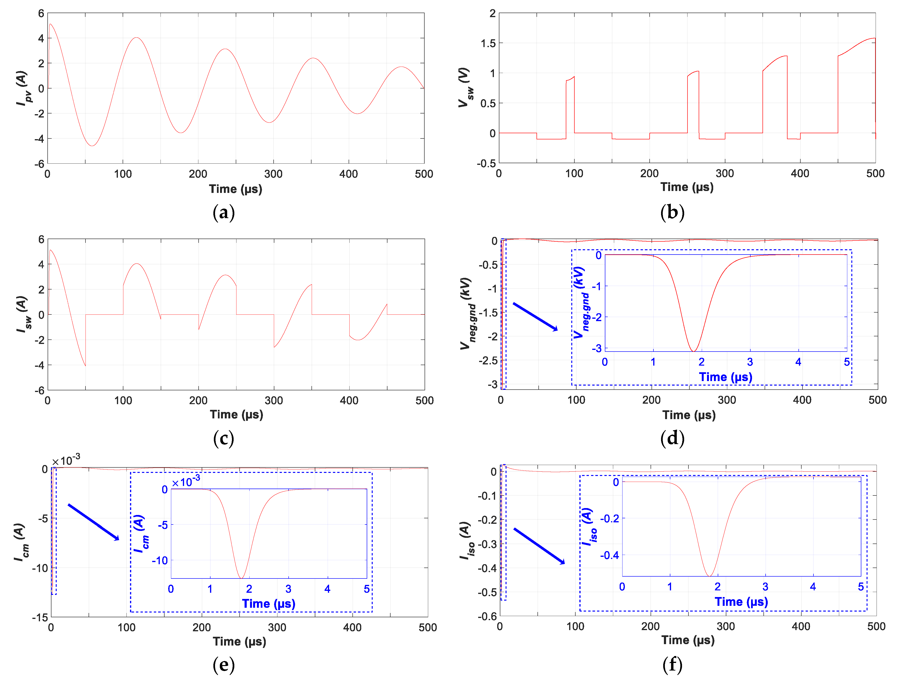
5.3.1. Reference Case

As a reference case, we assumed the values reported in Table 3, corresponding to a high value of PV module insulation, and a PV operating condition (module voltage bias) providing MPP. Furthermore, it was considered a vertical LC with a first short-stroke waveform for an aluminum frame. The switching frequency for the switch of the DC/DC converter was 10 kHz, and simulation ended at t = 500 μs.
Figure 11 reports the voltages induced in the frame and module for the reference case. Note that the actual output voltage available at PV terminal, Vpv, was due to the cumulative effect of directly induced voltage Vmod and the effect of coupling with current induced in the metallic frame Ifra, which shielded the direct lightning-induced voltage. Coherently with the nature of the induction phenomenon, the front time of voltages are imposed by the fast dynamic of the strike current (see Figure 4a).
The results in Figure 11 disclose that under common-mode, voltages up to some 1.76 kV can be induced in the single-PV module. If we consider the surge withstand capability (SWC) of live parts of a PV module [2,7], it is difficult to predict that insulation failures in the PV module can be caused by inductive couplings of nearby lightning strikes.
Figure 12 shows the voltages and currents induced in some of the remaining components of interface circuitry for the reference case. Regarding DC/DC converter, in spite of the voltage and current induced across the switch being within the converter switch limits (data in Figure 12b,c, respectively), the voltage to ground of the negative output terminal (that related with differential-mode, Figure 12d) can reach quite high values (−3.12 kV), leading to the breakdown of the SWC of the DC/DC converter [2,80].
Note that while the waveforms of the induced voltage at the PV module (Figure 11) were essentially imposed by the fast dynamic of the lightning current, the waveforms of current and voltage in the remaining components of the assembly (Figure 12) followed a slow dynamic imposed by the DC/DC converter filtering elements. In addition, the current does flow in the switch only when it is in the “on” state, as it was easily predictable. Reduced voltages show up at switch terminals during state transitions at the inset of induced current, while slower dynamics appear in the late phases, when the dynamic is dictated by the filtering elements in the DC/DC converter.

5.3.2. Sensitivity Analysis with Respect to Parameter Change

To appraise the impact of the different parameters of PV module model, describing relevant aspects of PV behavior, we varied some relevant circuit parameters. For each case of parameter change, as previously stated, Table 6 reports peak magnitude value and times associated with the monitored variables. The parameters that were changed are: (i) parameters of the PV high-frequency dynamic model, dependent on PV operating conditions; (ii) material of the frame; (iii) PV module insulation. In the following subsections, a detailed result analysis for each change is shown.
(i) Sensitivity to the dynamic module model parameters:
Since the values Cp,PVm and Rp,PVm of the dynamic model of PV module are a function of the operating voltage, two common PV operating conditions, different to that of the reference case (MPP), were selected, namely, the output (Vout) was configured for OC and SC condition, see Table 4. For these cases, we assumed the following values (all the other parameters remained equal).
The impact of the change in the PV operating condition on voltages and currents induced was negligible when the MPP and OC conditions were compared; see Table 6. Furthermore, a marginal increase could be observed at SC condition, possibly affected by the short-circuit current flow path.
(ii) Sensitivity to the frame material:
We considered the possibility of using a steel frame (ρ = 2.6 × 10⁻⁷ Ωm) instead of an aluminum frame (ρ = 2.6 × 10⁻⁸ Ωm). Therefore, the only varied parameter in the circuit is the frame resistance Rfra to a new value of 13 mΩ.
This parameter impacts on the frame current, and consequently the effective lightning voltage induced on the module was as follows
V e . m o d = V m o d M f r a m o d d I f r a d t
where M f r a m o d is the mutual inductance parameter, equal to M f r a mod = L f r a · L f r a (=2.63 mH) (assuming, as indicated above a coupling factor k = 1, as the PV circuitry concatenates all the magnetic flux produced by I f r a ).
Note that in the lower limit of the frequency band 1–5 MHz, relevant to the studied phenomenon, the imaginary part of the impedance would be ω·Lfra = 2π × 1.0 × 106 × 3.0 × 10−6 = 18.84 Ω, in any case much larger than the real part Rfra. Consequently, in the case of a steel frame, the impact is quite low, as can be seen from Table 6, reporting all peak values and decay times.
(iii) Sensitivity to the PV module insulation:
We analyzed the effect of the value change in the PV module insulation (insulation resistance and leakage capacitance between the frame and the active electrical circuitry of the module), see Table 5. A low value of PV module insulation (low resistance and high capacitance) may be due solely to material ageing or rain, mist or liquefied frost on the back surface of the module [36]. These phenomena impact insulation parameters Rs,iso,PVm, Rp,iso,PVm, and Cp,iso,PVm.
The impact of insulation change was moderate; see Table 6. There was a 20% decrease in the inducted voltage of module and an 8% drop for the ground voltage. Induced currents decreased to a lesser extent (between 8% and 13%), except for the module insulation current, which obviously increased by 5.88 times. This change underlines the relevance of the capacitance coupling appearing in the event of (partial) loss of insulation that change the behavior dominated by the inductive coupling between the active electrical circuitry of the module and frame at high insulation levels.

5.3.3. Influence of the Lightning Current Waveform

To assess the impact of possible subsequent short strokes, still hitting the ground 5 m away from the PV module, we considered a lightning current waveform with the subsequent short stroke parameters (see Table 1, Figure 4b).
The waveforms of voltages and currents induced throughout the converter-PV module assembly are reported in Figure 13 and Figure 14, while peak magnitude values and different times associated are reported in Table 7.
As expected, a major influence on the induced voltages can be observed, both on the peak value and times (e.g., front time); see Table 7. Peak value for the module voltage (Figure 13) and the voltage of the negative output terminal to ground (Figure 14d) increased up to 220% against the reference case. Furthermore, currents related with ground, i.e., Icm, Iiso, dominated by the much more relevant capacitance coupling, also increased in the same order. However, the peak value of other currents (Ipv, Figure 14a and Isw, Figure 14c) decreased by 39.3% in the case of a subsequent short stroke. A peak value drop also occurred for switch voltage (Figure 14b), but was limited by up to 19%. These reductions in the magnitude of currents and voltage can be explained by the dynamics imposed by the DC/DC converter filtering elements.

5.3.4. Impact of the LC Tortuous Geometry

In previous sections, the effect of a vertical lightning strike hitting at 5 m from the PV module was analyzed. Since the proposed method can explicitly consider the random tortuous nature of the lightning channels, and is prompt enough to perform a statistical analysis, to demonstrate the impact of tortuosity, several random paths of each strike were generated, and their effects were computed and averaged. Example waveforms for six different LC paths (case A to case F) are reported in Figure 15, while the expected values and standard deviations for the 100 cases are reported in Table 8.
From the statistical analysis, it can be noted that tortuosity leads to a non-negligible increase in the peak values in the variables, impacting both on circuit currents and voltages, achieving up to 23% for most variables, except for switch voltage, which only reaches a 10% increase. The standard deviation values suggest that the statistical variability of the channel geometry cannot be neglected when dimensioning the lightning protection system. Consequently, it is evident that the channel geometry plays a primary role in the assessment of the electromagnetic stress on a PV module. The hypothesis of a straight strike channel may lead to underestimation of its effects.

6. Conclusions

In a previous paper, we presented a 3D semi-analytical model that was able to calculate the lightning-induced transient overvoltage in a single PV module, considering capacitive and inductive couplings between the internal circuit of PV module and its metallic frame. The current research has extended our previous work by proposing an improved modelling for the PV module that includes both a high-frequency model of the module, the insulation model and a model for the connected DC/DC converter. The choice of typical value setting in the relevant parameters was based on an exhaustive review of the literature.
The connection of a DC/DC converter, usually adopted to link the PV module/s to external circuitry, allowed us to assess the effects of the nearby lightning strikes not only on the PV module, but also on the voltage and current outputs of the converter-PV module assembly.
Results for the reference case show that induced common-mode overvoltage in the PV module is within its SWC. However, regarding the DC/DC converter, in spite of induced currents being within the converter switch limits, the potential to ground of the output negative terminal could reach quite high values, leading to the breakdown of the electrical insulation of the DC/DC converter. Therefore, the proposed numerical simulation can help to understand under which circumstances the lightning-induced overvoltages exceed the SWC of each element in the PV assembly, helping to establish appropriate lightning and surge protection schemes. In addition, while the dynamics of induced overvoltages on PV module were essentially imposed by the lightning current, slower dynamics were observed in the current waveforms in the PV assembly due to the filtering elements in the DC/DC converter circuitry.
The comprehensive sensitivity analysis on the PV module parameters conclusively revealed a low influence of the PV operating condition on the induced overvoltages, as a result of the change in the parameters of the PV high-frequency dynamic model. Furthermore, the insignificance of the value setting of other parameters, such as the material of the frame, was highlighted. In contrast, the PV module insulation (dependent on meteorological conditions) was found to have a moderate impact on results. There was a 20% decrease in inducted voltages when low-insulation conditions were assessed. The sensitivity analysis of external factors to the modelling of converter-PV module assembly, e.g., the influence of lightning current waveform determined by comparing a subsequent short stroke vs. first short stroke that the associated faster dynamics induced higher overvoltages in the PV module (increase up to 221%), and higher potentials to ground (up to 220%), while currents in the DC/DC converter circuitry were smaller (a reduction of about 40%). Following with external factors, a further statistical analysis with respect to the lightning channel geometry allowed to conclude that the usual vertical strike assumption may lead to underestimating the effect of indirect lightning. A reduction in inducted voltages and currents of 20% was computed on average.
On the other hand, photovoltaic modules hardly come alone, so the next step in this study is the simulation of indirect lightning effects on full photovoltaic arrays, considering capacitive couplings among frames and mutual interactions among different modules. A detailed description of the connection to system ground does represent a further improvement to also be considered, in order to correctly account for the overvoltage appearing at output pins when the protections to ground (e.g., Zener diodes) are neglected.

Author Contributions

Conceptualization, A.F., J.C.H., C.P. and F.S.-S.; methodology, A.F., J.C.H., and C.P.; software, A.F., C.P. and F.S.-S.; validation, A.F., J.C.H., C.P. and F.S.-S.; formal analysis, A.F., J.C.H., C.P. and F.S.-S.; investigation, A.F., J.C.H., C.P. and F.S.-S.; resources, A.F., J.C.H., C.P. and F.S.-S.; data curation, A.F., J.C.H., C.P. and F.S.-S.; writing—original draft preparation, A.F. and J.C.H.; writing—review and editing, A.F. and J.C.H.; visualization, A.F., J.C.H., C.P. and F.S.-S.; supervision, A.F., J.C.H., C.P. and F.S.-S.; project administration, A.F. and J.C.H.; funding acquisition, A.F. and J.C.H. All authors have read and agreed to the published version of the manuscript.

Funding

This research was funded by the Agencia Estatal de Investigación, Spain (AEI) and the Fondo Europeo de Desarrollo Regional (FEDER) aimed at the Challenges of Society (Grant No. ENE 2017-83860-R “Nuevos servicios de red para microredes renovables inteligentes. Contribución a la generación distribuida residencial”).

Informed Consent Statement

Informed consent was obtained from all subjects involved in the study.

Data Availability Statement

Not applicable.

Conflicts of Interest

The authors declare no conflict of interest.

Abbreviations

a, b, c, dfitting parameters
A ( r ¯ s , t ) magnetic vector potential at point r ¯ s and time t due to a lightning strike segment
Acmcommon-mode area
Admdifferential-mode area
Afframe area
c free space light velocity
Cboostcapacitance in the LC filter of the DC/DC boost converter
CD,PVcdiffusion capacitance of a PV cell
Cknumber of arbitrarily oriented segments of the LC
Cp,iso,PVmleakage capacitance of a PV module
C p , P V c parallel capacitance of a PV cell
C p , P V m parallel capacitance of a PV module
CT,PVctransition capacitance of a PV cell
Dduty cycle
ffrequency
fsswitching frequency
h channel height
I 0 ( t ) return stroke current waveform at channel base
I 1 ( I 2 ) current at the positive (negative) output terminal of the DC/DC converter
I c m   common mode current at the terminals of the DC/DC converter
I d m   differential mode current at the terminals of the DC/DC converter
I g photocurrent
I p e a k peak value of the lightning current waveform
IGBTinsulated-gate bipolar transistor
Iisomodule insulation current
I o u t output current of the DC/DC converter
Iswcurrent through the switch
l f r a total length of the four frame sides
kcoupling factor
Loverall length of the LC
Lboostinductance in the LC filter of the DC/DC boost converter
LC lightning channel
Ldc,w(Lpv,w)parasitic inductance of the connecting wires at the converter’s DC side (at PV module)
Lfraframe equivalent self-inductance
Lgndground path inductance
L m average length of each segment average of the LC
Lsseries inductance of cables and connectors
Mfra-modmutual inductance of metallic frame with the PV circuitry
MPP maximum power point
nexponent factor
OC open-circuit
PV photovoltaic
P ( r , φ , z ) observation point
rradial distance of observation point P
r ¯ s position vector of observation point P
Rboostresistance in the LC filter of the DC/DC boost converter
Rd,PVcdynamic resistance of diode of a PV cell
Rdc,w(Rpv,w)parasitic resistance of the connecting wires at the converter’s DC side (at PV module)
R f r a frame equivalent resistance
Rgndground path resistance
Riso,PVminsulation resistance of a PV module
RLoadload resistance
Rp,iso,PVmparallel insulation resistance of a PV module
Rp,PVc (Cp,PVc)parallel resistance (capacitance) of a PV cell
R p , P V m parallel resistance of a PV module
R r distance between infinitesimal current dipole and observation point P
Rsseries resistance of cables and connectors
Rs,PVcseries resistance of a PV cell
R s , P V m series resistance of a PV module
Rsh,PVcshunt resistance of a PV cell
Rs,iso,PVmseries insulation resistance of a PV module
Rsw,onresistance in series with ideal switch
Rsw,sh(Csw,sh)resistance (capacitance) connected in parallel to the with ideal switch
Rsw,.gnd(Csw,gnd)shunt resistance (stray shunt capacitance) between the aluminum radiator of IGBT module and the ground
SC short-circuit
S C C shape equivalent section of a PV metallic frame
t time
u Heaviside step function
v velocity of propagation of return stroke current
V P V c voltage bias of a PV cell
V c m   common mode voltage at the terminals of the DC/DC converter
V d m   differential mode voltage at the terminals of the DC/DC converter
Ve.modeffective module voltage due to frame effect
V f r a equivalent voltage source simulating the coupling of the LC with the conducting frame (frame voltage)
V i n input voltage of the DC/DC converter
V m o d equivalent voltage source simulating the coupling of the LC with the module inner electrical circuitry (module voltage)
V n e g . g n d ( V p o s . g n d ) voltage of negative (positive) output terminal to ground
V p v PV output voltage
V s w switch voltage
ω angular frequency
z height of an infinitesimal current dipole
Z g n ground path impedance
Z P V m   dynamic impedance of the PV module in dark conditions
Δ I L b o o s t current ripple of the DC/DC converter
Δ V C b o o s t voltage ripple of the DC/DC converter
Δϕaverage absolute value of the angle between adjacent segments
ηcorrection factor
μ 0 vacuum permeability
ρmaterial resistivity
τ1rise time
τ2decay time
φazimuth of a generic observation point P
Γequivalent line for the cell interconnections

References

  1. Formisano, A.; Petrarca, C.; Hernández, J.C.; Muñoz-Rodríguez, F.J. Assessment of induced voltages in common and differential-mode for a PV module due to nearby lightning strikes. IET Renew. Power Gener. 2019, 13, 1369–1378. [Google Scholar] [CrossRef]
  2. Hernández, J.C.; Gómez-Vidal, P.; Jurado, F. Lightning and Surge Protection in Photovoltaic Installations. IEEE Trans. Power Deliv. 2008, 23, 1961–1971. [Google Scholar] [CrossRef]
  3. Zhang, Y.; Chen, H.C.; Du, Y. Lightning protection design of solar photovoltaic systems: Methodology and guidelines. Electr. Power Syst. Res. 2019, 174, 105877. [Google Scholar] [CrossRef]
  4. Zhang, Y.; Chen, H.C.; Du, Y. Considerations of Photovoltaic System Structure Design for Effective Lightning Protection. IEEE Trans. Electromagn. Compat. 2020, 62, 1333–1341. [Google Scholar] [CrossRef]
  5. Uman, M.A. All about Lightning; Dover: Toronto, ON, Canada, 1986; pp. 1–158. [Google Scholar]
  6. Belik, M. PV panels under lightning conditions. In Proceedings of the 2014 15th International Scientific Conference on Electric Power Engineering (EPE), Brno, Czech Republic, 12–14 May 2014; pp. 367–370. [Google Scholar]
  7. Jiang, T.; Grzybowski, S. Electrical degradation of Photovoltaic modules caused by lightning induced voltage. In Proceedings of the 2014 IEEE Electrical Insulation Conference (EIC), Philadelphia, PA, USA, 8–11 June 2014; pp. 107–110. [Google Scholar]
  8. Kokkinos, N.; Christofides, N.; Charalambous, C.A. Lightning protection practice for large-extended photovoltaic installations. In Proceedings of the 2012 International Conference on Lightning Protection (ICLP), Vienna, Australia, 2–7 September 2012; pp. 1–5. [Google Scholar]
  9. NEDO. Analysis and Evaluation of Lightning Damage Condition and Damage Decrease Countermeasure Technique of Lightning Damage for PV Systems; NEDO: Tokyo, Japan, 2009. [Google Scholar]
  10. Lightning Protection of Low-Voltage Networks; CIGRE WG C4.408; CIGRE Technical Brochure: Paris, France, 2013.
  11. Yang, H.; Liu, X. Design of PV charge and discharge controller in insulator monitoring system. In Proceedings of the 2011 2nd International Conference on Artificial Intelligence, Management Science and Electronic Commerce (AIMSEC), Dengleng, China, 8–10 August 2011; pp. 2039–2042. [Google Scholar]
  12. Ahmad, N.; Ab-Kadir, M.; Izadi, M.; Azis, N.; Radzi, M.; Zaini, N.; Nasir, M. Lightning protection on photovoltaic systems: A review on current and recommended practices. Renew. Sustain. Energy Rev. 2018, 82, 1611–1619. [Google Scholar] [CrossRef]
  13. Hernández, Y.M.; Ioannidis, D.; Ferlas, G.; Giannelaki, E.; Tsovilis, T.E.; Politis, Z.; Samaras, K. An experimental approach of the transient effects of lightning currents on the overvoltage protection system in MW-class photovoltaic plants. In Proceedings of the 2014 International Conference on Lightning Protection (ICLP), Shanghai, China, 11–18 October 2014; pp. 1972–1977. [Google Scholar]
  14. Yamamoto, K.; Takami, J.; Okabe, N. Overvoltages on DC Side of Power Conditioning System Caused by Lightning Stroke to Structure Anchoring Photovoltaic Panels. Electr. Eng. Jpn. 2014, 187, 29–41. [Google Scholar] [CrossRef]
  15. Higo, T.; Matsuda, K.; Nagaoka, N. Transient electromagnetic induction into a PV panel. In Proceedings of the 2014 49th International Universities Power Engineering Conference (UPEC), Cluj-Napoca, Romania, 2–5 September 2014; pp. 1–5. [Google Scholar]
  16. Stern, H.-J.; Karner, H.C. Lightning induced EMC phenomena in photovoltaic modules. In Proceedings of the 1993 International Symposium on Electromagnetic Compatibility, Dallas, TX, USA, 9–13 August 1993; pp. 442–446. [Google Scholar]
  17. Sakai, K.; Yamamoto, K. Lightning protection of photovoltaic power generation system: Influence of grounding systems on overvoltages appearing on DC wirings. In Proceedings of the 2013 International Symposium on Lightning Protection (XII SIPDA), Belo Horizonte, Brazil, 7–11 October 2013; pp. 335–339. [Google Scholar]
  18. Charalambous, C.A.; Kokkinos, N.; Christofides, N.; Ab Kadir, M.Z.A.; Gomes, C. A simulation tool to assess the lightning induced over-voltages on dc cables of photovoltaic installations. In Proceedings of the 2014 International Conference on Lightning Protection (ICLP), Shanghai, China, 11–18 October 2014; pp. 1571–1576. [Google Scholar]
  19. Sekioka, S. An experimental study of sparkover between a rod and a photovoltaic panel. In Proceedings of the 2012 International Conference on Lightning Protection (ICLP), Vienna, Austria, 2–7 September 2012; pp. 1–5. [Google Scholar]
  20. Haberlin, H.; Minkner, R. A simple method for lightning protection of PV-systems. In Proceedings of the 2th European Photovoltaic Solar Energy Conference and Exhibition, Amsterdam, The Netherlands, 14–18 February 1994; pp. 1–4. [Google Scholar]
  21. Haeberlin, H. Interference voltages induced by magnetic fields of simulated lightning currents in photovoltaic modules and arrays. In Proceedings of the 17th European Photovoltaic Solar Energy Conference, Munich, Germany, 22–26 October 2001; pp. 1–4. [Google Scholar]
  22. Coetzer, K.M.; Wiid, P.G.; Rix, A.J. PV Installation Design Influencing the Risk of Induced Currents from Nearby Lightning Strikes. In Proceedings of the 2019 International Conference on Clean Electrical Power (ICCEP), Otranto, Italy, 2–4 July 2019; pp. 204–213. [Google Scholar]
  23. Mendez, Y.; Acosta, I.; Rodriguez, J.C.; Ramirez, J.; Bermudez, J.; Martinez, M. Effects of the PV-generator’s terminals connection to ground on electromagnetic transients caused by lightning in utility scale PV-plants. In Proceedings of the 2016 33rd International Conference on Lightning Protection (ICLP), Estoril, Portugal, 25–30 September 2016; pp. 1–8. [Google Scholar]
  24. Zhang, C.; Tu, Y.; Hu, J.; Sun, W.; Li, H.J.; Wang, S. Study of induced overvoltage on solar arrays. In Proceedings of the 2011 7th Asia-Pacific International Conference on Lightning, Chengdu, China, 1–4 November 2011; pp. 852–857. [Google Scholar]
  25. Tu, Y.; Zhang, C.; Hu, J.; Wang, S.; Sun, W.; Li, H. Research on lightning overvoltages of solar arrays in a rooftop photovoltaic power system. Electr. Power Syst. Res. 2013, 94, 10–15. [Google Scholar] [CrossRef]
  26. Yonezawa, K.; Mochizuki, S.; Takahashi, Y.; Idogawa, T.; Morii, N.; Yonezawa, K. Evaluation of SPDs for a PV system using the FDTD method taking concrete foundations into consideration. In Proceedings of the 2014 International Conference on Lightning Protection (ICLP), Shanghai, China, 11–18 October 2014; pp. 1091–1094. [Google Scholar]
  27. Karim, M.R.; Ahmed, R. Analysis of Electromagnetic Induction due to Lightning on a Large-Scale Solar Power Generation. In Proceedings of the 2019 International Conference on Electrical, Computer and Communication Engineering (ECCE), Cox’sBazar, Bangladesh, 7–9 February 2019; pp. 1–5. [Google Scholar]
  28. Hossain, A.; Ahmed, R. Analysis of indirect lightning phenomena on solar power system. J. Electr. Eng. 2014, 21, 127–133. [Google Scholar] [CrossRef]
  29. Benesova, Z.; Haller, R.; Birkl, J.; Zahlmann, P. Overvoltages in photovoltaic systems induced by lightning strikes. In Proceedings of the 2012 International Conference on Lightning Protection (ICLP), Vienna, Austria, 2–7 September 2012; pp. 1–6. [Google Scholar]
  30. Dechthummarong, C.; Thepa, S.; Chenvidhya, D.; Jivacate, C.; Kirtikara, K.; Thongpron, J. Lightning impulse test of field-aged PV modules and simulation partial discharge within MATLAB. In Proceedings of the 2012 9th International Conference on Electrical Engineering/Electronics, Computer, Telecommunications and Information Technology, Phetchaburi, Thailand, 16–18 May 2012; pp. 1–4. [Google Scholar]
  31. Jiang, T.; Grzybowski, S. Impact of lightning impulse voltage on polycrystalline silicon photovoltaic modules. In Proceedings of the 2013 International Symposium on Lightning Protection (XII SIPDA), Belo Horizonte, Brazil, 7–11 October 2013; pp. 287–290. [Google Scholar]
  32. Ahmad, N.I.; Ab-Kadir, M.Z.A.; Izadi, M.; Zaini, N.H.; Radzi, M.A.M.; Azis, N.; Hasan, W.Z.W. On the performance of a polycrystalline PV panel under different impulse voltages and temperatures. In Proceedings of the 2016 33rd International Conference on Lightning Protection (ICLP), Estoril, Portugal, 25–30 September 2016; pp. 1–6. [Google Scholar]
  33. Naxakis, I.; Christodoulou, C.; Perraki, V.; Pyrgioti, E. Degradation effects on single crystalline silicon photovoltaic modules subjected to high impulse-voltages. IET Sci. Meas. Technol. 2017, 11, 563–570. [Google Scholar] [CrossRef]
  34. Naxakis, I.; Pyrgioti, E.; Perraki, V.; Tselepis, E. Studying the effect of the impulse voltage application on sc-Si PV modules. Sol. Energy 2017, 144, 721–728. [Google Scholar] [CrossRef]
  35. Charalambous, C.A.; Kokkinos, N.D.; Christofides, N. External Lightning Protection and Grounding in Large-Scale Photovoltaic Applications. IEEE Trans. Electromagn. Compat. 2013, 56, 427–434. [Google Scholar] [CrossRef]
  36. Hernández, J.C.; Gómez-Vidal, P.; Medina, A. Characterization of the insulation and leakage currents of PV generators: Relevance for human safety. Renew. Energy 2010, 35, 593–601. [Google Scholar] [CrossRef]
  37. Dechthummarong, C.; Chenvidhya, D.; Jivacate, C.; Kirtikara, K. Experiment and simulation impulse partial discharge behavior in dielectric encapsulations of field-aged PV modules. In Proceedings of the 2011 37th IEEE Photovoltaic Specialists Conference, Experiment and Simulation Impulse Partial Discharge Behavior in Dielectric Encapsulations of Field-Aged PV Modules, Seattle, WA, USA, 19–24 June 2011; pp. 003109–003112. [Google Scholar]
  38. Deshmukh, M.; Kumar, R.A.; Nagaraju, J. Measurement of solar cell ac parameters using the time domain technique. Rev. Sci. Instrum. 2004, 75, 2732–2735. [Google Scholar] [CrossRef]
  39. Limsakul, C.; Chenvidhya, D.; Kirtikara, K. PV impedance characterization using square wave method and frequency response analyser. In Proceedings of the 31st Photovoltaic Science and Engineer Conference and Solar Energy Exhibition, Hamburg, Germany, 14–18 September 2015; pp. 3109–3112. [Google Scholar]
  40. Kumar, R.; Suresh, M.; Nagaraju, J. Silicon (BSFR) solar cell AC parameters at different temperatures. Sol. Energy Mater. Sol. Cells 2005, 85, 397–406. [Google Scholar] [CrossRef]
  41. Kumar, S.; Sareen, V.; Batra, N.; Singh, P.K. Study of C–V characteristics in thin n+-p-p+ silicon solar cell sandinduced junction n-p-p+ cell structures. Sol. Energy Mater. Sol. Cells 2010, 94, 1469–1472. [Google Scholar] [CrossRef]
  42. Kim, K.A.; Krein, P.T.; Seo, G.-S.; Cho, B.-H. Photovoltaic AC parameter characterization for dynamic partial shading and hot spot detection. In Proceedings of the 2013 Twenty-Eighth Annual IEEE Applied Power Electronics Conference and Exposition (APEC), Long Beach, CA, USA, 17–21 March 2013; pp. 109–115. [Google Scholar]
  43. Chenvidhya, D.; Kirtikara, K.; Jivacate, C. PV module dynamic impedance and its voltage and frequency dependencies. Sol. Energy Mater. Sol. Cells 2005, 86, 243–251. [Google Scholar] [CrossRef]
  44. Pongklang, T.; Chenvidhya, D.; Kirtikara, K.; Chuangchote, S.; Silsirivanich, N. Voltage and Frequency Dependent Impedances of Dye-sensitized Solar Cell. Energy Procedia 2014, 52, 536–540. [Google Scholar] [CrossRef] [Green Version]
  45. Chayavanich, T.; Limsakul, C.; Chayavanich, N.; Chenvidhya, D.; Jivacate, C.; Kirtikara, K. Describing dynamic behavior of static iv characteristics of pv modules using dynamic impedance. In Proceedings of the 21st European Photovoltaic Solar Energy Conference, Dresden, Germany, 4–8 September 2006; pp. 1–2. [Google Scholar]
  46. Poon, J.; Jain, P.; Spanos, C.; Panda, S.K.; Sanders, S.R. Photovoltaic condition monitoring using real-time adaptive parameter identification. In Proceedings of the 2017 IEEE Energy Conversion Congress and Exposition (ECCE), Cincinnati, OH, USA, 1–5 October 2017; pp. 1119–1124. [Google Scholar]
  47. Kareem, M.S.A.; Saravanan, M. A new method for accurate estimation of PV module parameters and extraction of maximum power point under varying environmental conditions. Turk. J. Electr. Eng. Comput. Sci. 2016, 24, 2028–2041. [Google Scholar] [CrossRef]
  48. Omicron-Lab. Available online: https://www.omicron-lab.com (accessed on 4 December 2020).
  49. Chayavanich, T.; Limsakul, C.; Chayavanich, N.; Chenvidhya, D.; Jivacate, C.; Kirtikara, K. Voltage and frequency dependent model for PV module dynamic impedance. In Proceedings of the 17th International Photovoltaic Science & Engineering Conference, Fukuoka, Japan, 3–7 December 2007; pp. 1–4. [Google Scholar]
  50. Panigrahi, J.; Vandana; Singh, R.; Batra, N.; Gope, J.; Sharma, M.; Pathi, P.; Srivastava, S.; Rauthan, C.; Singh, P. Impedance spectroscopy of crystalline silicon solar cell: Observation of negative capacitance. Sol. Energy 2016, 136, 412–420. [Google Scholar] [CrossRef]
  51. Bharadwaj, P.; Kulkarni, A.; John, V. Impedance estimation of photovoltaic modules for inverter start-up analysis. Sadhana 2017, 42, 1377–1387. [Google Scholar] [CrossRef]
  52. Eshappa, T.; Ranjan, R.; Ghatpande, N.D. Modeling of solar array and analyze the current transient response of shunt switch voltage regulator in spacecraft power conditioning unit. J. Adv. Comput. Commun. Technol. 2015, 3, 33–39. [Google Scholar]
  53. Matsuda, K.; Nagaoka, N.; Higo, T.; Namba, A. A simple lumped-equivalent circuit of a photovoltaic panel for transient simulations. In Proceedings of the 2014 49th International Universities Power Engineering Conference (UPEC), Cluj-Napoca, Romania, 2–5 September 2014; pp. 1–5. [Google Scholar]
  54. Nariman, M. Diagnosis of Photovoltaic Modules using Alternate Methods of Measurement. Bachelor’s Thesis, Czech Technical University in Prague, Prague, Czech Republic, 2017. [Google Scholar]
  55. Chenvidhya, D.; Kirtikara, K.; Jivacate, C. A new characterization method for solar cell dynamic impedance. Sol. Energy Mater. Sol. Cells 2003, 80, 459–464. [Google Scholar] [CrossRef]
  56. Kumar, R.; Suresh, M.; Nagaraju, J. GaAs/Ge solar cell AC parameters at different temperatures. Sol. Energy Mater. Sol. Cells 2003, 77, 145–153. [Google Scholar] [CrossRef]
  57. Chenvidhya, D.; Kirtikara, K.; Jivacate, C. Dynamic impedance characterization of solar cells and PV modules based on frequency and time domain analysis. In Trends in Solar Energy Research; Nova Science Publishers, Inc.: New York, NY, USA, 2006; pp. 21–45. [Google Scholar]
  58. Kumar, R.A.; Suresh, M.S.; Nagaraju, J. Facility to measure solar cell ac parameters using an impedance spectroscopy technique. Rev. Sci. Instrum. 2001, 72, 3422–3426. [Google Scholar] [CrossRef]
  59. Cotfas, P.A.; Cotfas, D.T.; Borza, P.N.; Sera, D.; Teodorescu, R. Solar Cell Capacitance Determination Based on an RLC Resonant Circuit. Energies 2018, 11, 672. [Google Scholar] [CrossRef] [Green Version]
  60. Jha, V.; Triar, U.S. An Improved Generalized Method for Evaluation of Parameters, Modeling, and Simulation of Photovoltaic Modules. Int. J. Photoenergy 2017, 2017, 2532109. [Google Scholar] [CrossRef] [Green Version]
  61. Yu, S.; Wang, J.; Zhang, X.; Li, F. Complete Parasitic capacitance model of photovoltaic panel considering the rain water. Chin. J. Mech. Electr. Eng. 2017, 3, 77–84. [Google Scholar]
  62. Sabiha, N.A.; Alsharef, M.; Metwaly, M.K.; Elattar, E.E.; Taha, I.B.; Abd-Elhady, A.M. Sustaining electrification service from photovoltaic power plants during backflow lightning overvoltages. Electr. Power Syst. Res. 2020, 186, 106386. [Google Scholar] [CrossRef]
  63. Di Piazza, M.C.; Viola, F.; Vitale, G. Evaluation of ground currents in a PV system with high frequency modeling. Int. J. Renew Energy Res. 2018, 8, 1770–1778. [Google Scholar]
  64. Petrarca, C.; Minucci, S.; Andreotti, A. On the influence of channel tortuosity on electric fields generated by lightning return strokes at close distance. Prog. Electromagn. Res. B 2017, 74, 61–75. [Google Scholar] [CrossRef] [Green Version]
  65. Lupo, G.; Vitelli, M.; Petrarca, C.; Tucci, V. EM fields generated by lightning channels with arbitrary location and slope. IEEE Trans. Electromagn. Compat. 2000, 42, 39–53. [Google Scholar] [CrossRef]
  66. Idone, V.P.; Orville, R.E. Channel tortuosity variation in Florida triggered lightning. Geophys. Res. Lett. 1988, 15, 645–648. [Google Scholar] [CrossRef]
  67. Protection against Lightning: General Principles; IEC Standard 62305-1; IEC: London, UK, 2010.
  68. Hernández, J.C.; Gómez-Vidal, P. Guidelines for Protection Against Electric Shock in PV Generators. IEEE Trans. Energy Convers. 2009, 24, 274–282. [Google Scholar] [CrossRef]
  69. Chiariello, A.G.; Formisano, A.; Martone, R. A high-performance computing procedure for the evaluation of 3D coils inductance. COMPEL Int. J. Comput. Math. Electr. Electron. Eng. 2015, 34, 248–260. [Google Scholar] [CrossRef]
  70. Chen, H.C.; Du, Y. Model of ferromagnetic steels for lightning transient analysis. IET Sci. Meas. Technol. 2018, 12, 301–307. [Google Scholar] [CrossRef]
  71. Leban, K.; Ritchie, E. Selecting the accurate solar panel simulation model. In Proceedings of the 2008 Nordic Workshop on Power and Industrial Electronics, Espoo, Finland, 9–11 June 2008. [Google Scholar]
  72. Nishioka, K.; Sakitani, N.; Uraoka, Y.; Fuyuki, T. Analysis of multicrystalline silicon solar cells by modified 3-diode equivalent circuit model taking leakage current through periphery into consideration. Sol. Energy Mater. Sol. Cells 2007, 91, 1222–1227. [Google Scholar] [CrossRef]
  73. Pierret, R.F. Semiconductor Device Fundamentals; Addison-Wesley Publishing Company, Inc.: New York, NY, USA, 1996. [Google Scholar]
  74. Khamis, A.; Mohamed, A.; Shareef, H.; Ayob, A. Modeling and simulation of small scale microgrid system. Aust. J. Basic Appl. Sci. 2012, 6, 412–421. [Google Scholar]
  75. Manitoba, H. Battery System a Generic Example, PSCAD/EMTDC: Electromagnetic Transients Program Including DC Systems; Manitoba HVDC Research Centre: Winnipeg, MB, Canada, 1994. [Google Scholar]
  76. MURS320 Diode. Available online: https://www.mouser.es/datasheet/2/115/ds30197-87238.pdf (accessed on 28 December 2020).
  77. RF05VYM2S Diode. Available online: https://fscdn.rohm.com/en/products/databook/datasheet/discrete/diode/fast_recovery/rf05vym2sfh.pdf (accessed on 28 December 2020).
  78. Ibrahim, H.; Anani, N. Evaluation of Analytical Methods for Parameter Extraction of PV modules. Energy Procedia 2017, 134, 69–78. [Google Scholar] [CrossRef]
  79. Alqahtani, A.H. A simplified and accurate photovoltaic module parameters extraction approach using matlab. In Proceedings of the 2012 IEEE International Symposium on Industrial Electronics, Hangzhou, China, 28–31 May 2012; pp. 1748–1753. [Google Scholar]
  80. Insulation Coordination for Equipment within Low-Voltage Supply Systems: Principles, Requirements and Tests; IEC Standard 60664-1; IEC: London, UK, 2020.
Figure 1. Geometrical model of the tortuous lightning channel (LC).
Electronics 10 00120 g001
Figure 2. Vertical lightning channel.
Electronics 10 00120 g002
Figure 3. Arbitrarily oriented channel segment.
Electronics 10 00120 g003
Figure 4. Lightning current waveforms according to IEC 62305-1 [67]: (a) first negative short stroke for lightning protection level (LPL) I; (b) subsequent negative short stroke for LPL I.
Electronics 10 00120 g004
Figure 5. 270 Wp-PV module investigated.
Electronics 10 00120 g005
Figure 6. Lightning channel coupling model for the PV module.
Electronics 10 00120 g006
Figure 7. DC and dynamic models of the active electrical circuitry for a PV cell.
Electronics 10 00120 g007
Figure 8. Equivalent circuit model for the insulation of a PV module [36].
Electronics 10 00120 g008
Figure 9. DC/DC boost converter circuit.
Electronics 10 00120 g009
Figure 10. Full circuitry model for PV module and DC/DC converter assembly.
Electronics 10 00120 g010
Figure 11. Reference case, induced voltages at the PV module. Vertical lightning channel with a first short stroke waveform hitting 5 m away from the module for an aluminum frame.
Electronics 10 00120 g011
Figure 12. Reference case, voltages and currents induced in some of the remaining components of interface circuitry: (a) PV current output; (b) switch voltage; (c) current across the switch; (d) voltage of negative output terminal to ground; (e) common mode current; (f) module insulation current.
Electronics 10 00120 g012
Figure 13. Case of subsequent short stroke, induced voltages at the PV module. Vertical strike hitting 5 m away from the module.
Electronics 10 00120 g013
Figure 14. Case of subsequent short stroke, induced voltages and currents in some of the remaining components of interface circuitry: (a) PV current output; (b) switch voltage; (c) current across the switch; (d) voltage of negative output terminal to ground; (e) common mode current; (f) module insulation current.
Electronics 10 00120 g014
Figure 15. Case of various channel tortuosity, voltages and currents induced in some components of converter-PV module assembly: (a) induced voltages at the PV module; (b) PV current output; (c) switch voltage; (d) current across the switch; (e) voltage of negative output terminal to ground; (f) module insulation current.
Electronics 10 00120 g015
Table 1. Parameters for lightning current waveforms, first short stroke and subsequent short stroke.
ParameterFirst Negative Short StrokeSubsequent Negative Short Stroke
Peak current: Ipeak (kA)10050
Exponent factor: n1010
Correction factor: η0.9860.993
Rise time: τ1 (µs)190.454
Decay time: τ2 (µs)485143
Table 2. Value setting adopted for parameters in simulations (Irradiation: 100 W/m2; frequency: 1 MHz).
ParameterUnitsVoltage Operating Conditions
Short-Circuit (SC)Maximum Power Point (MPP)Open-Circuit (OC)
Rp,PVm117.6 [42]35.6 [42]2.0 [42,46,47,60,78,79]
Cp,PVmμF0.46 [42]1.36 [23,42,45,46]1.57 [42]
ParameterUnitsValueParameterUnitsValue
Rs,PVm807 [23,60]RgndΩ0.1 [62]
Rfra1.3 [1,3] Rboost1.0 [63]
LfraμH3.0 [1,3]LboostμH250 [63]
Cp,iso,PVmnF3.7–179.2 [23,36,62]CboostμF200 [63]
Rp,iso,PVm0.38–14.93 [36]Rsw,onμΩ1.0
Rs,iso,PVm0.003–2.980 [36,68]Rsw,shΩ100
LsμH2.29 [3,51,52,53,62]Csw,shnF1.0
Rs150 [3,46]Rsw,gnd250 [62,63]
Rpv,w (=Rdc,w)50 [47,63]Csw,gndpF0.15 [62,63]
Lpv,w (=Ldc,w)μH0.05 [47,63]RLoadΩ50
LgndμH1.0 [62]
Table 3. Value setting adopted for parameters in the reference case (irradiation: 100 W/m2; frequency: 1 MHz; high PV module insulation; MMP condition).
ParameterUnitsReference ValueParameterUnitsReference Value
2*Rp,iso,PVm30Cp,PVmμF
2*Rs,iso,PVm6.0Rs,PVm800
Cp,iso,PVm/2nF2.0LsμH2.3
Rp,PVm36Rs150
Table 4. Value setting adopted for parameters in simulations at OC and SC conditions.
ParameterUnitsVoltage Operating Condition
OCSC
Rp,PVm2.0120
Cp,PVmμF1.60.5
Rs,PVm800
Table 5. Value setting adopted for parameters in simulations at low insulation condition.
ParameterUnitsLow Insulation
2*Rp,iso,PVm0.8
2*Rs,iso,PVmΩ6.0
Cp,iso,PVm/2nF90
Table 6. Sensitivity analysis on voltages and currents induced with the parameter change in the PV module model.
Considered VariationVpvVswVneg.gndIpvIswIcmIiso
Peak Value
(V)
Decay Time
(μs)
Front Time
(μs)
Half Value Time
(μs)
Peak Value
(V)
Peak Value
(V)
Decay Time
(μs)
Front Time
(μs)
Half Value Time
(μs)
Peak Value
(A)
Decay Time
(μs)
Peak Value
(A)
Peak Value
(A)
Peak Value
(A)
Reference case1759.12.5831.7112.1731.58–3116.41.8301.7122.1755.13943.65.13–0.013–0.518
Operating condition: OC1759.12.5831.7112.1741.11–3116.51.8301.7122.1755.13878.25.13–0.013–0.518
Operating condition: SC1760.42.5821.7112.1742.60–3117.11.8301.7122.1755.121409.85.12–0.013–0.518
Steel frame1753.82.5681.7132.1701.56–3111.01.8301.7132.1735.07941.65.07–0.013–0.517
Low PV insulation1408.52.6831.7182.1391.54–2978.71.8301.7432.1714.51950.04.51–0.012–304.6
Table 7. Sensitivity analysis for induced voltages and currents for different lightning current waveforms.
Considered VariationVpvVswVneg.gndIpvIswIcmIiso
Peak Value
(V)
Decay Time
(μs)
Front Time
(μs)
Half Value Time
(μs)
Peak Value
(V)
Peak Value
(V)
Decay Time
(μs)
Front Time
(μs)
Half Value Time
(μs)
Peak Value
(A)
Decay Time
(μs)
Peak Value
(A)
Peak Value
(A)
Peak Value
(A)
First short stroke (Reference case)1759.12.5831.7112.1731.58–3116.41.8301.7122.1755.13943.65.13–0.013–0.518
Subsequent short stroke3890.17.5400.3860.6331.27–6886.14.7600.3860.6343.117827.83.117–0.032–1.168
Table 8. Expected values and standard deviations for induced voltages and currents for various tortuosity cases.
Considered VariationVpvVswVneg.gndIpvIswIcmIiso
Peak Value
(V)
Decay Time
(μs)
Front Time
(μs)
Half Value Time
(μs)
Peak Value
(V)
Peak Value
(V)
Decay Time
(μs)
Front Time
(μs)
Half Value Time
(μs)
Peak Value
(A)
Decay Time
(μs)
Peak Value
(A)
Peak Value
(A)
Peak Value
(A)
Reference case1759.12.5831.7112.1731.58–3116.41.8301.7122.1755.13943.65.13–0.013–0.518
Tortuosity casesExpected value2165.22.2191.6272.2311.747–3811.41.8251.6302.2296.319808.66.319–0.015–0.634
Standard variation196.80.9780.0030.0030.082332.80.0020.0040.0030.582356.50.5820.0010.055
Publisher’s Note: MDPI stays neutral with regard to jurisdictional claims in published maps and institutional affiliations.

