Article

Common-Mode Voltage Reduction Algorithm for Photovoltaic Grid-Connected Inverters with Virtual-Vector Model Predictive Control

1
School of Electrical Engineering, Guangxi University, Nanning 530004, China
2
School of Electronics and Computer Science, University of Southampton Malaysia, Iskandar Puteri 79200, Johor, Malaysia
3
College of Environment and Ecology, Xiamen University, Xiamen 361102, China
4
Department of Technology Management, Faculty of Construction Management and Business, University Tun Hussein Onn Malaysia, Parit Raja 86400, Johor, Malaysia
*
Author to whom correspondence should be addressed.
Electronics 2021, 10(21), 2607; https://doi.org/10.3390/electronics10212607
Submission received: 3 August 2021 / Revised: 5 October 2021 / Accepted: 20 October 2021 / Published: 25 October 2021
(This article belongs to the Section Power Electronics)

Abstract

:
Model predictive control (MPC) has been proven to offer excellent model-based, highly dynamic control performance in grid converters. The increasingly higher power capacity of a PV inverter has led to the industrial preference of adopting higher DC voltage design at the PV array (e.g., 750–1500 V). With high array voltage, a single stage inverter offers advantages of low component count, simpler topology, and requiring less control tuning effort. However, it is typically entailed with the issue of high common-mode voltage (CMV). This work proposes a virtual-vector model predictive control method equipped with an improved common-mode reduction (CMR) space vector pulse width modulation (SVPWM). The modulation technique essentially subdivides the hexagonal voltage vector space into 18 sub-sectors, that can be split into two groups with different CMV properties. The proposal indirectly increases the DC-bus utilization and extends the overall modulation region with improved CMV. The comparison with the virtual-vector MPC scheme equipped with the conventional SVPWM suggests that the proposed technique can effectively suppress 33.33% of the CMV, and reduce the CMV toggling frequency per fundamental cycle from 6 to either 0 or 2 (depending on which sub-sector group). It is believed that the proposed control technique can help to improve the performance of photovoltaic single-stage inverters.

1. Introduction

Solar photovoltaic (PV) energy generation, wind energy generation, and other new energy technologies are constantly being developed. Control and modulation techniques of voltage source inverter (VSI), which is the main physical interface between renewable energy sources and the power grid, have garnered considerable research attention [1]. In standard MPC schemes, the use of all actual voltage vectors inherently results in elevated CMV. On the other hand, MPC schemes with SVPWM uses virtual vector vectors and the CMV performance depends primarily on the modulation design. High peak CMV and frequent toggling of CMV of converters may reduce the system reliability, posing potential safety concerns [2,3].
Numerous research works on CMV suppression have been reported to date. In general, these solutions on CMV performance can be categorized into hardware-based and software-based techniques. In the hardware-based solutions, CMV is typically mitigated by incorporating a passive filter or optimizing the voltage source inverter topology [4,5]. However, this approach necessitates additional hardware, resulting in higher maintenance effort and costs. On the other hand, software-based CMV suppression methods can be subdivided further into those based on direct control scheme and those based on pulse width modulation (PWM). In the direct control group, e.g., direct MPC with actual voltage vectors, it is common to augment the cost objective into considering CMV as a cost component [6,7]. These approaches necessitate the design of a suitable weight factor to balance the various cost components in the cost function. L. Guo et al. suggests an MPC scheme with preselected voltage vectors having low CMV [8,9]. However, the preselection has limited the amount of voltage vectors available, and therefore results in a higher harmonic distortion. MPC-based CMV suppression methods have been studied in conjunction with various inverter topologies [10,11,12].
PWM modulation techniques can be modified to restrain CMV. For example, the CMV can be suppressed by only using either odd or even voltage vectors [13]. However, the corresponding DC-bus utilization factor is very poor. In addition, non-zero voltage vector modulation approaches, such as active zero-state switch PWM [2], near-state PWM [14,15], and remote-state PWM [16] have been reported in the past. Moreover, [17,18] compare the performance indices of various modulation schemes, in terms of e.g., CMV amplitude, output THD. Table 1 summarizes the advantages and disadvantages of the proposed techniques. Moreover, other CMV-related works have attempted to improve other inverter efficiency indicators, such as switching losses [15,19], restraining common-mode electromagnetic interference [20], or leakage current in photovoltaic grid-connected inverter [21,22]. Furthermore, [23] suggests a hybrid modulation based on the modulation magnitude, resulting in varying CMV performance. Another hybrid modulation is studied in [24] but it requires a common-mode inductor, which increases the system cost and design complexity. In [25], an enhanced discontinuous modulation is proposed to reduce the line switching loss while suppressing CMV. However, if the switching sequences in the subdivided sectors of the hexagonal voltage vector space can be ordered more optimally, further improvement may be achieved. There are other simplified PWM techniques [26,27,28], each with respective merits and demerits. Similarly, PWM-based CMV improvement have been studied in conjunction with different inverter topologies [29,30,31,32].
This paper’s contribution is as follows: (1) In the proposed improved common-mode reduction space vector pulse width modulation (CMRSVPWM) with 18 sub-sectors organizes the switching sequences in each sub-sector into resulting lower CMV amplitude and oscillation frequency; (2) MPC uses a large amount of virtual voltage vectors, such that all the 18 subsectors can be fully utilized. By combining the virtual vector MPC and CMRSVPWM, the CMV performance of the single-stage inverter can be improved.
The following is the structure of the article: Section 2 introduces the mathematical model and MPC for a three-phase two-level photovoltaic inverter, together with the standard SVPWM and its CMV property. Section 3 proposes the virtual vector MPC with the improved CMRSVPWM modulation, where the details of division, vector selection, and CMV amplitude and frequency are described. Section 4 compares the performance with the standard SVPWM and the proposed CMRSVPWM method using simulation studies. Section 5 summarizes and concludes the overall findings. Section 6 provides proposes directions for future work. The Appendix A contains two tables. Table A1 shows the definition of acronym. Meanwhile, Table A2 shows the definition of notations in this paper.

2. Virtual-Vector MPC

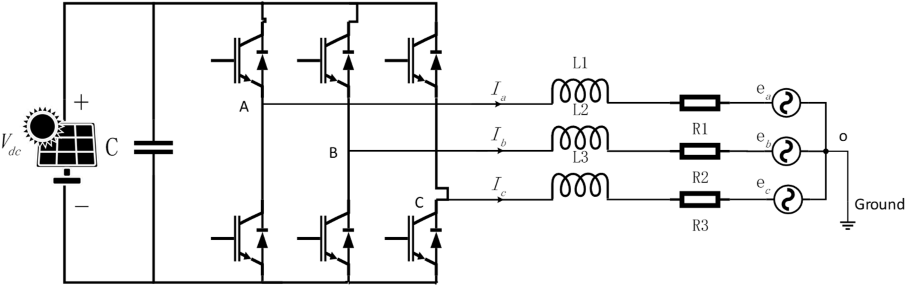
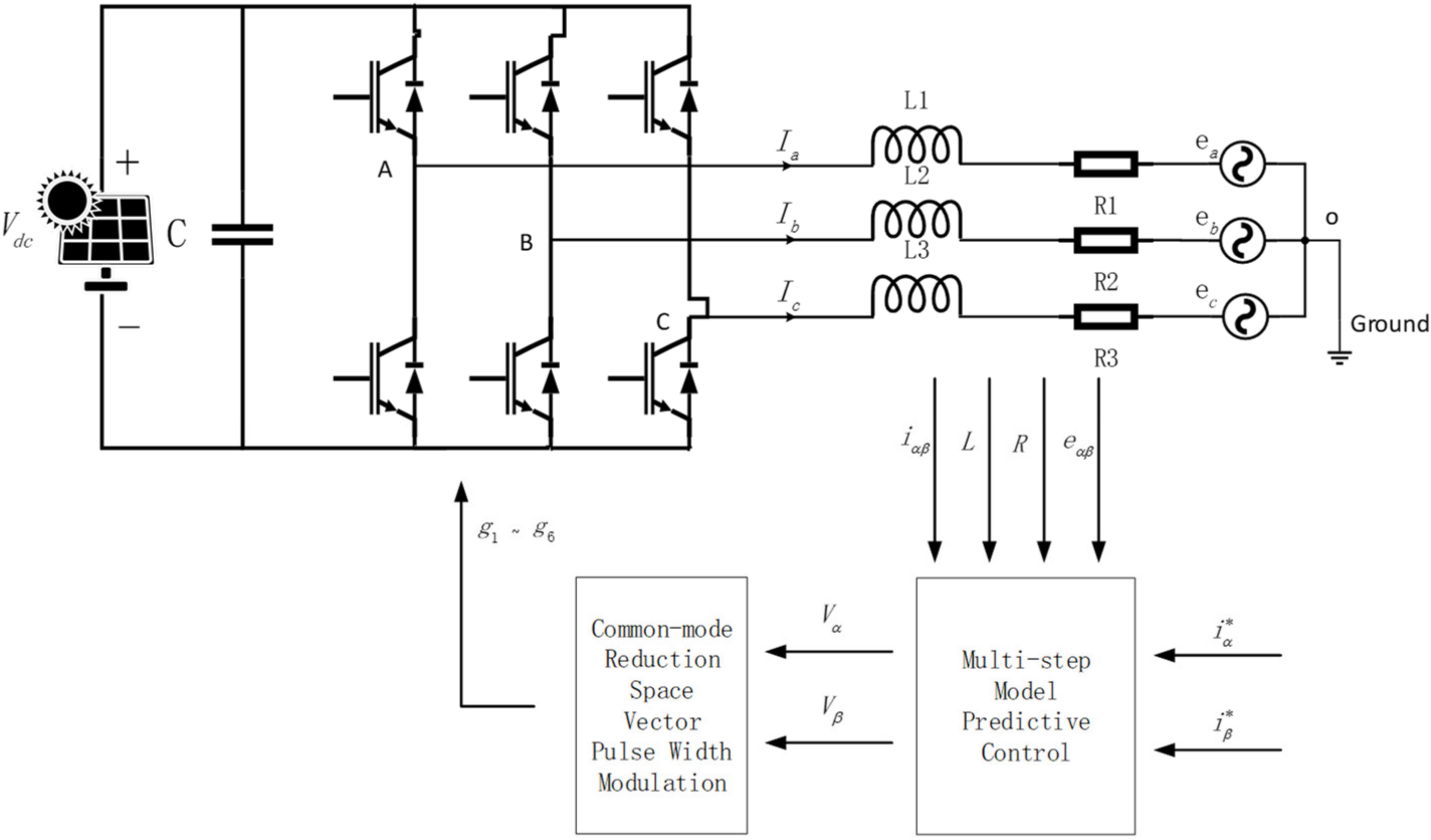
2.1. Three-Phase PV VSI Model

Figure 1 shows the topology of the three-phase two-level single-stage photovoltaic inverter that is connected to a three-phase grid (emulated using ideal three-phase source). As described, this topology is relevant to photovoltaic application with high DC array voltage (e.g., 750 V to 1500 V).
In Figure 1, V d c is the output voltage of PV array, V a , V b and V c are the inverter output voltages, L and R are filter inductor and its internal resistance, and e a , e b , and e c are the emulated AC grid voltages. Point O is the grounded neutral of the AC grid. The plant under control can be represented by the set of Equation (1):
V a = L d i a d t + R i a + e a V b = L d i b d t + R i b + e b V c = L d i c d t + R i c + e c
Through Clarke transformation, the circuit voltage equations are transformed from the three-phase coordinate to the α β two-phase stationary coordinate, giving Equation (2):
L d i α d t = V α R i α e α L d i β d t = V β R i β e β
Each symbol in Equation (2) has the same meanings as defined above, but now the α β coordinate. Since the PV inverter contains three sets of switches, they are capable of producing a total of eight switching states. The relationship between the output voltages and the switching states can be described by Equation (3), where parameter a defines the unit vector that introduces 120 ° phase difference among phases:
V i = 2 3 V d c S a + a S b + a 2 S c a = e j 2 π 3 = 1 2 + j 3 2     i = 0 , 1 7  
where V i represents the output voltage obtainable from different switching stats, S a , S b , and S c represent, respectively, the states of each switch, and V d c is the DC-bus voltage. The combination of these eight switching states corresponds to eight actual/basic voltage vectors that can be denoted as V 0 ~ V 7 . V 0 and V 7 are zero voltage vectors, and the other six are non-zero voltage vectors, with the same amplitude, but different phase angles.

2.2. Model Predictive Control of VSI

Using forward-Euler method to discretize the grid current model [9]:
i α k + 1 = 1 R T s + L L i α k + T s V α k T s e α k i β k + 1 = 1 R T s + L L i β k + T s V β k T s e β k
where i α k + 1 and i β k + 1 are the predicted values of α β -axis currents at (k + 1)th time instant, i α k and i β k are the α β -axis current feedback at kth sampling instant, T s is the sampling period in seconds, and e α k and e β k are the α β -axis grid voltage at kth sampling instant.
Standard single-vector MPC analyzes only eight actual voltage vectors per control cycle to identify the switching state with the lowest cost value. If the control sampling frequency is insufficiently high, three-phase currents will suffer from higher harmonics. To improve this aspect, virtual voltage vectors, or sub-voltage vectors, are considered in this study.
It has been well-established that the inherent digital implementation delay has to be compensated in MPC implementation in conjunction with power electronic application. Two-step ahead prediction technique is utilized to compensate the inherent delay [6]. With this two-step MPC, the cost function can be written as Equation (5):
g = i α * i α k + 2 + i β * i β k + 2
where i α * and i β * are the reference values of the α β -axis currents that can be obtained from inverse-Clarke transformed of synchronous-axis current. i α k + 2 and i β k + 2 are the α β -axis currents at (k + 2)th instant.

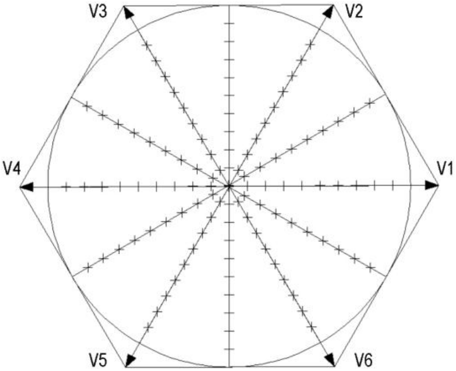
2.3. CMV of Basic Voltage Vectors

Equation (6) is used to calculate the PV inverter’s CMV without regard for the DC side’s midpoint voltage fluctuation [35]:
V c m v = V a o + V b o + V c o / 3
where V a o ( V b o and V c o ) is the voltage between the phase-A (phase-B and phase-C) output of the inverter and the DC neutral point. Table 2 summarizes the CMV induced by the switching combinations. CMV has four values, ± V d c / 2 and ± V d c / 6 , where the two of the zero voltage vectors have the highest peak CMV.

2.4. Conventional Modulation Method

In the conventional SVPWM, six non-zero vectors naturally divide into six equilateral triangular sectors S 1 ~ S 6 in the α β -plane, which is shown in Figure 2a. Using the first sector as an example, Figure 2b illustrates how a voltage vector can be synthesized from the actual voltage vectors.
Under the sector S 1 , the action times of each vector can be calculated according to the volt-second principle, as in Equation (7) [35]:
T P W M V r e f = T 1 V 1 + T 2 V 2 + T 0 V 0 + T 7 V 7 T P W M = T 1 + T 2 + T 0 + T 7
where T P W M is the sampling time of one control/PWM cycle, V r e f is the reference voltage vector, V 0 , V 1 , V 2 , and V 7 are the voltage vectors selected for synthesis, and T 0 , T 1 , T 2 and T 7 are the corresponding action time periods. T 0 and T 7 are typically equal.
In Table 2, the highest CMV is V d c / 2 because SVPWM employs zero voltage vectors. In what follows, we introduce AZSPWM [2], NSPWM [14], and RSPWM [16]—these PWM techniques share the common feature of suppressing the CMV amplitude and toggling frequency. Figure 3 illustrates an example of synthesized switching waveforms for each of the aforementioned modulation techniques and the associated CMV.

3. Proposed CMRSVPWM Methods for VSI

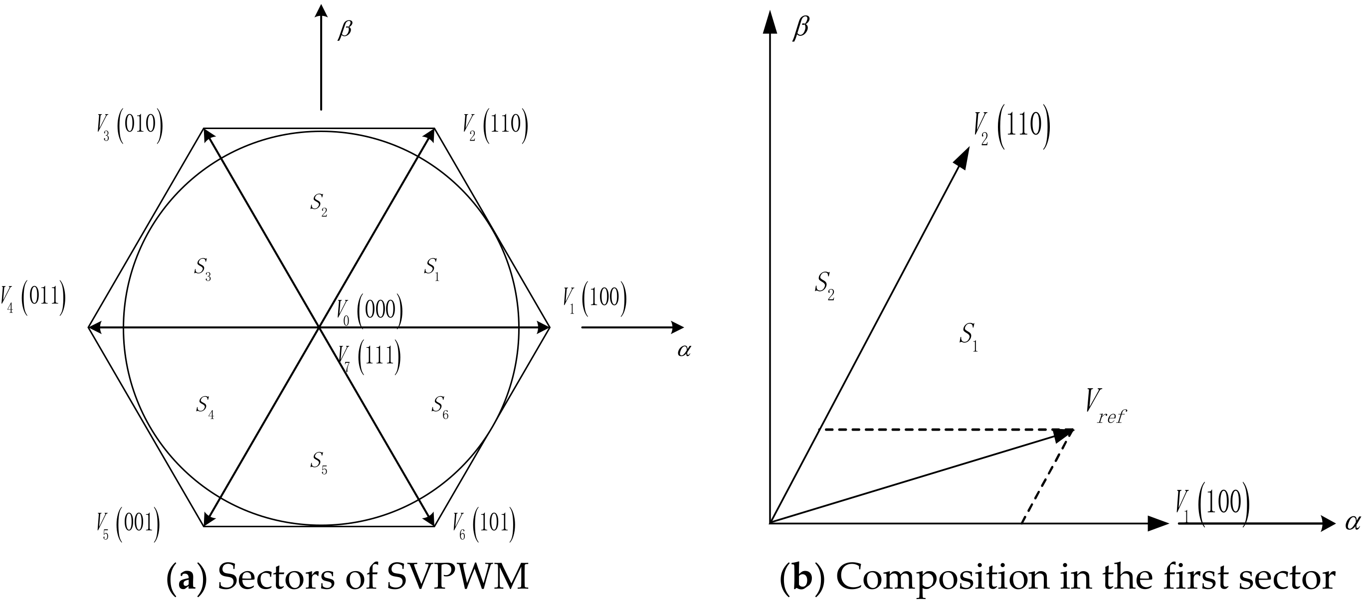
3.1. Sectors of CMRSVPWM
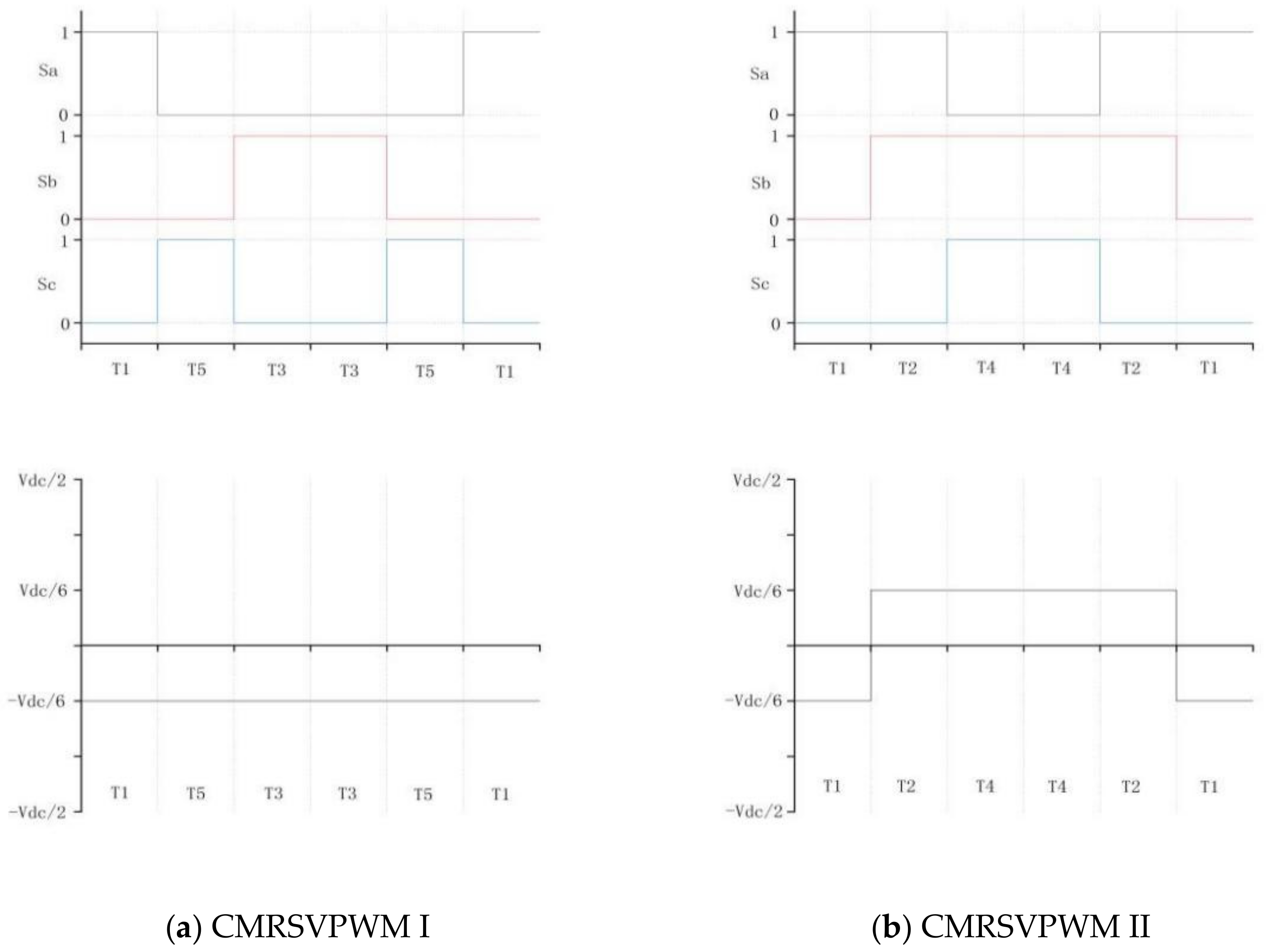
In order to reduce the amplitude and toggling frequency of CMV and increase the DC-bus utilization, CMRSVPWM is proposed in this work.
It begins with subdividing the basic six sectors, then divides each basic sector into three parts. The two sections vertex at the origin have the same modulation index range, so they are combined into the first component of CMRSVPWM (CMRSVPWM I), which forms the hexagonal star shape. The remaining six triangular areas are the second portion of CMRSVPWM (CMRSVPWM II). Modulation index determines which of the regions should be used. Note that since each of the six sub-regions of CMRSVPWM I contains two basic sectors, it is important to determine the precise location of the reference voltage vector. Figure 4 shows that the angle between two sector boundaries that can be used to decide whether odd or even voltage vectors are used in the synthesis process.
SVPWM that uses only odd or even vectors for synthesis will result in a very-low DC-bus utilization rate. Figure 5a shows that the DC-bus utilization rate, which is essentially equal to the radius r 1 ( = V d c / 3 ) of the inner tangent circle of the middle-side triangle. CMRSVPWM I in this work intends to improve this aspect. Figure 5b shows the maximum linear output voltage is now increased to radius r 2 ( = 2 3 V d c / 9 ), which is the inner tangent circle of the hexagonal star shape. The DC-bus utilization of CMRSVPWM I is increased by 15.47%, as compared to the scheme with either odd or even vectors, while continuing to suppress the CMV peak amplitude.

3.2. CMRSVPWM I

The action times of voltage vector can be solved using the volt-second principle. Modulation index Mi is introduced in Equation (8) [35]:
M i = π V r e f 2 V d c
The action times corresponding to the voltage vector V 1 ~ V 6 are T 1 ~ T 6 . The general equations that solve for the action times are shown in Equation (9).
T 1 = ( 1 / 3 + 2 M i c o s θ / π ) T P W M T 3 = ( 1 / 3 M i c o s θ / π + 3 M i s i n θ / π ) T P W M T 5 = ( 1 / 3 M i c o s θ / π 3 M i s i n θ / π ) T P W M T 2 = ( 1 / 3 + M i c o s θ / π + 3 M i s i n θ / π ) T P W M T 4 = ( 1 / 3 2 M i c o s θ / π ) T P W M T 6 = ( 1 / 3 + M i c o s θ / π 3 M i s i n θ / π ) T P W M
Table 3 summarizes the switching sequences in each sector (clockwise direction is assumed).

3.3. CMRSVPWM II

Another main contribution of this work is to propose on the use of both CMRSVPWM I and CMRSVPWM II modes to address the problem of limited usable modulation index range in CMRSVPWM I alone, therefore improving the DC-bus utilization. This scheme that combines CMRSVPWM I and CMRSVPWM II into suppressing CMV is known as CMRSVPWM in what follows. With CMRSVPWM II mode, the DC-bus utilization is further increased from 2 3 V d c / 9 (in CMRSVPWM I) to 2 V d c / 3 as Figure 6 shows. The modulation index M i decides on which modes, I or II, to be used. Odd-even vectors mixing modulation is used to synthesize the reference voltage vector in CMRSVPWM II. Table 4 details the switch action sequences for each sector in the CMRSVPWM II.
Again, using the first sector for illustration, Figure 7 shows the synthesis of the both CMRSVPWM modes and the corresponding CMV. In theory, CMRSVPWM I has no CMV fluctuation, i.e., zero voltage toggling frequency, within a modulation cycle. CMRSVPWM II, on the other hand, manifests twice voltage change/toggling. Note that the CMV peak voltages in both modes are V d c / 6 .

4. Experimental Result and Discussion

The proposed MPC and CMRSVPWM methods are investigated using Matlab-Simulink. Figure 8 depicts the control loop. A 380 V 50 Hz AC grid is assumed. The DC-bus voltage is chosen to be 750 V, but it is noted that single-stage voltage source inverter typically have higher varying DC voltage, e.g., in the range of 750 V to 1500 V.

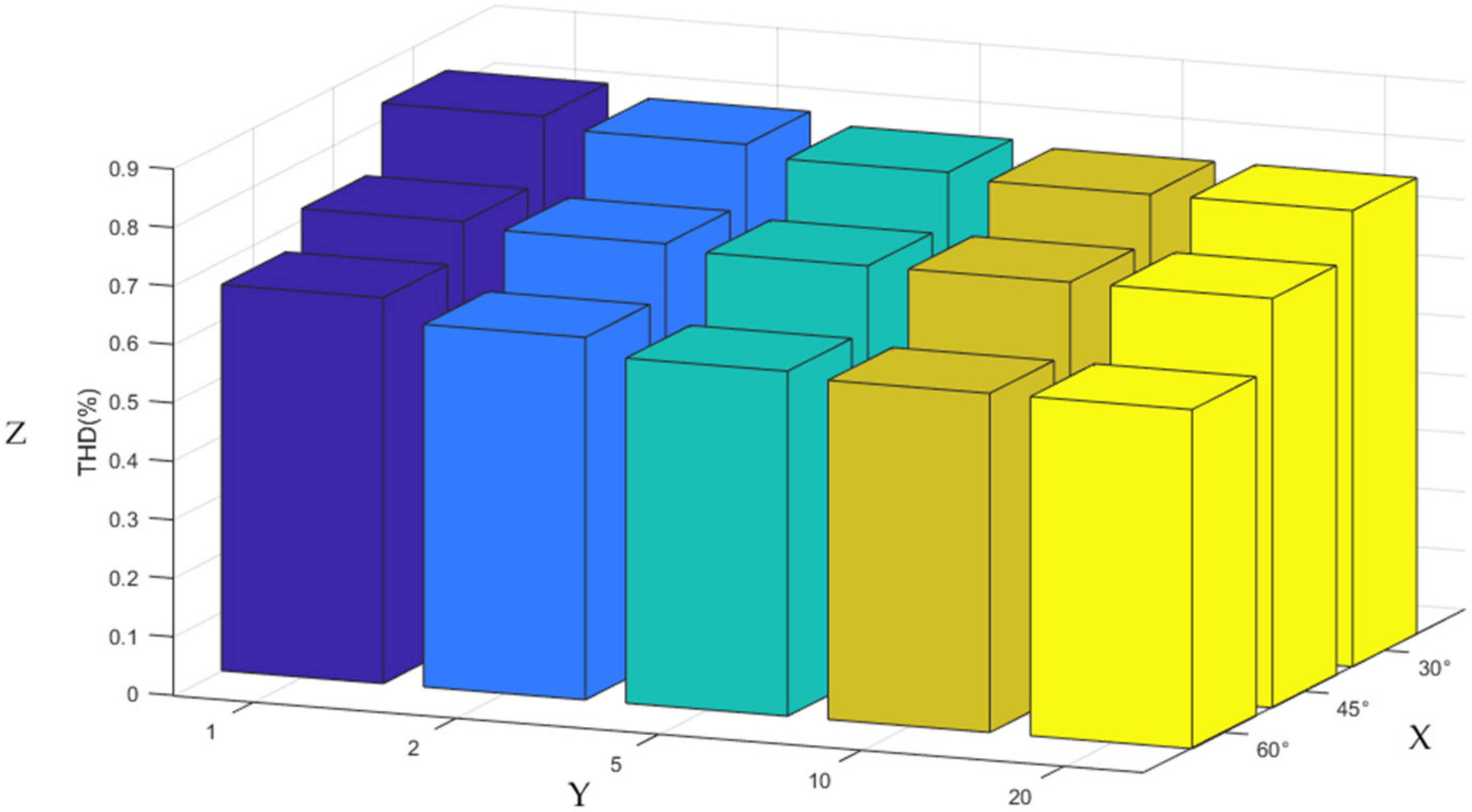
4.1. Virtual-Vector MPC
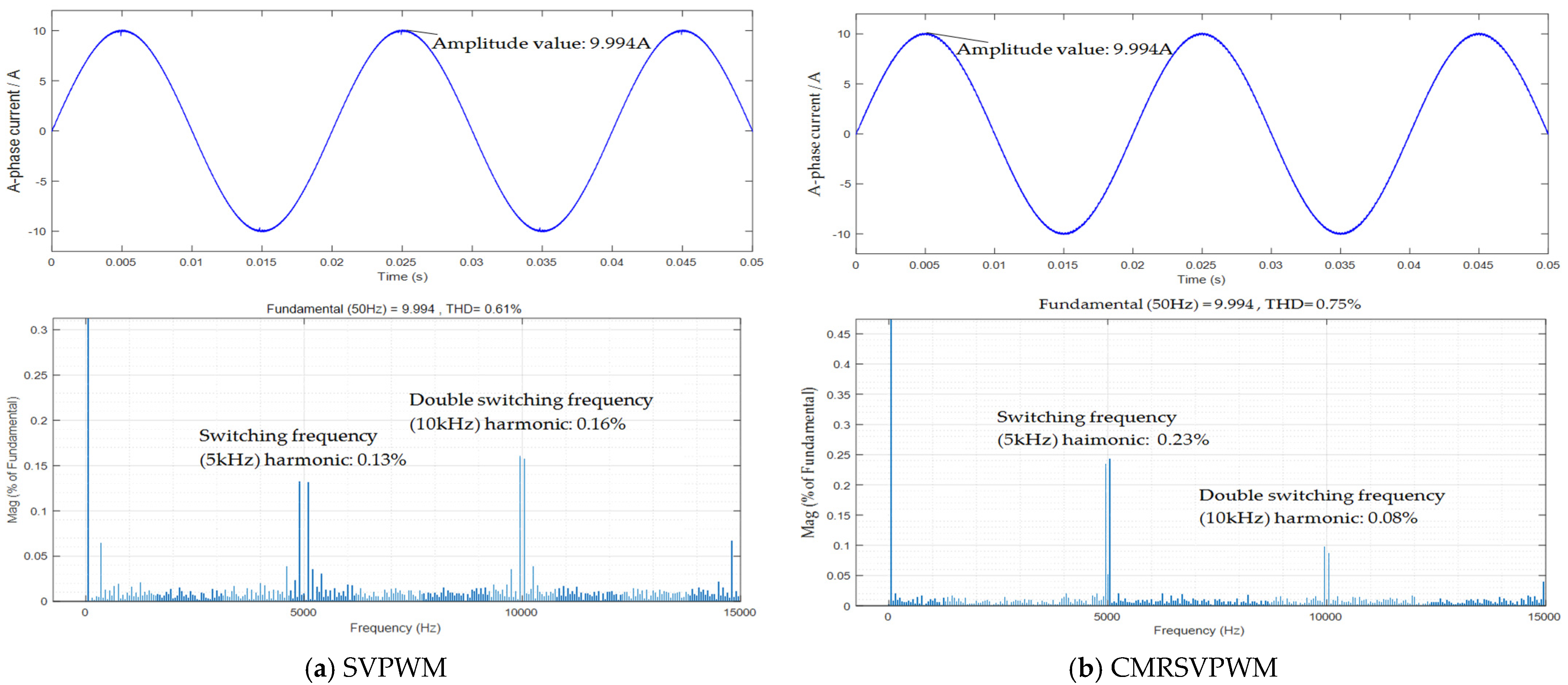
To fully utilize the entire voltage vector space, virtual vector MPC is used in this work. First, a range of selection of virtual vectors is investigated. Virtual voltage vectors are chosen at the angular phase angle intervals of 30, 45, and 60 degrees within the modulation limit. Then, each selected voltage vector is divided into 1, 2, 5, 10, and 20 sub-voltage vectors based on the magnitude length. The resulted THDs of these combinations are summarized in Figure 9.
When the interval angle is the same, selecting more sub-voltage vectors results in a lower THD value. When the same number of sub-voltage vectors (in each phase angle value) is used, the THD value decreases as the angle interval decreases. As shown in Figure 9, there is only a small different of 0.01% for the selections of 10 and 20 sub-voltage vectors. With the consideration of computational burden, the virtual voltage vectors with a 30-degree angle interval (around the hexagonal voltage vector space, as show in Figure 10) and ten sub-voltage vectors (equal, for each phase angle) are used in this work.

4.2. CMV Simulation

Table 5 describes the parameters used by the simulation model, and the inverter control part adopts the standard two-step ahead MPC method.
The comparison in Figure 11a,b shows that the simulation results are consistent with the theoretical analysis. The peak and valley values of CMV in conventional SVPWM are ± 375 V ( ± V d c / 2 ), while the peak and valley values of CMRSVPWM are ± 125 V ( ± V d c / 6 ), representing a decrease of 66.67%. Notably, CMRSVPWM has fewer CMV frequency jumps per fundamental cycle.
Phase-A current and its THD values for SVPWM and CMRSVPWM are shown in Figure 12a,b. Both have a period of 0.02 s and an amplitude of 9.994 A. Next, phase-A output voltages are compared in Figure 13a,b. The amplitudes of 311.4 V of the phase-A voltages are comparable for both.
Characteristics of several PWM techniques targeting CMV improvement, and that of the proposed CMRSVPWM I and CMRSVPWM II, are listed in Table 6. All techniques with improved CMV property can reduce the peak CMV to Vdc/6. Th proposed CMRSVPWM has the best combination of DC-bus utilization and CMV frequency (which is either 0 or 2, due to the two modes). For current THD (where only that for SVPWM, AZSPWM, NSPWM and CMRSVPWM are measured; all four modulation schemes have the same DC-bus utilization), and they have practically the same value, agreeing with theoretical expectation.

5. Conclusions

Space vector modulation is enhanced to reduce the property of the single-stage voltage source inverter. The following results are taken from the simulation experiment:
(1)
In comparison to the SVPWM, the enhanced CMRSVPWM strategy decreases the CMV amplitude from V d c / 2 to V d c / 6 , a reduction of 66.67%. The CMV toggling frequency is reduced to either 0 or 2.
(2)
In comparison with the PWM techniques with either three odd or three even vectors, the proposed CMRSVPWM I will increase the utilization rate of the DC bus by 15.47%, reaching 2 3 V d c / 9 . The utilization rate is increased further through CMRSVPWM II, up to the maximum available rate as that of SVPWM.
(3)
Through virtual-vector MPC with 120 sub-vectors, the entire range of CMRSVPWM can be utilized to output switching harmonic performance.

6. Deficiencies and Prospects

In actual implementation, a dead zone will manifest itself during the modulation phase. However, since the focus of this article is on the use of the proposed CMRSVPWM in conjunction with virtual-vector MPC, the dead zone is not considered. Future work will explore this issue in greater detail.

Author Contributions

Conceptualization, H.H.G. and X.L.; methodology, X.L. and C.S.L.; software, X.L.; validation, C.S.L.; formal analysis, D.Z. and W.D.; investigation, H.H.G.; writing—original draft preparation, X.L.; writing—review and editing, H.H.G., T.A.K. and K.C.G. All authors have read and agreed to the published version of the manuscript.

Funding

This research was funded by Guangxi University grant number A3020051008.

Conflicts of Interest

The authors declare that they have no known competing financial interests or personal relationships that could have appeared to influence the work reported in this paper.

Appendix A

Table A1. Definition of acronym in paper.
VSIVoltage Source InverterSVPWMSpace Vector Pulse Width Modulation
MPCModel Predictive ControlAZSPWMZero-State Switch Pulse Width Modulation
CMVCommon-Mode VoltageNSPWMNear-State Pulse Width Modulation
PWMPulse Width ModulationRSPWMRemote-State Pulse Width Modulation
THDTotal Harmonic DistortionCMRSVPWMCommon-Mode Reduction Space Vector Pulse Width Modulation
Table A2. Definition of notations in paper.
V d c Output voltage of PV i α β k + 2 Currents in k + 2 T s
V a b c Inverter output voltages i α β * Reference current values on α β axis
i a b c Inverter output currents T s Sampling time
e a b c Grid voltages L Filter value
i α β Output currents on α β coordinate system R Filter’s internal resistance
V i i = 0 , 1 7 Output voltage from different switching states V c m v Common-mode voltage value
a Phase difference of 120 ° V a o Voltage between the phase-A output of the inverter and the DC neutral point
S a b c States of switch T P W M Sampling time of one cycle
i α β k Feedback values of α β axis currents at the current time T i i = 0 , 1 7 Corresponding action times of voltage vectors
e α β k Grid voltage values of α β axis at the current moment M i Modulation index
i α β k + 1 Predicted values of α β axis currents at the next moment

References

  1. Ferreira, S.C.; Gonzatti, R.B.; Pereira, R.R.; da Silva, C.H.; da Silva, L.E.B.; Lambert-Torres, G. Finite Control Set Model Predictive Control for Dynamic Reactive Power Compensation with Hybrid Active Power Filters. IEEE Trans. Ind. Electron. 2018, 65, 2608–2617. [Google Scholar] [CrossRef]
  2. Jayaraman, K.; Kumar, M. Design of Passive Common-Mode Attenuation Methods for Inverter-Fed Induction Motor Drive With Reduced Common-Mode Voltage PWM Technique. IEEE Trans. Power Electron. 2020, 35, 2861–2870. [Google Scholar] [CrossRef]
  3. Chen, K.; Hsieh, M. Generalized Minimum Common-Mode Voltage PWM for Two-Level Multiphase VSIs Considering Reference Order. IEEE Trans. Power Electron. 2017, 32, 6493–6509. [Google Scholar] [CrossRef]
  4. Chen, X.; Xu, D.; Liu, F.; Zhang, J. A Novel Inverter-Output Passive Filter for Reducing Both Differential- and Common-Mode dv/dt at the Motor Terminals in PWM Drive Systems. IEEE Trans. Ind. Electron. 2007, 54, 419–426. [Google Scholar] [CrossRef]
  5. Duong, T.-D.; Nguyen, M.-K.; Tran, T.-T.; Lim, Y.-C.; Choi, J.-H.; Wang, C. Modulation Techniques for a Modified Three-Phase Quasi-Switched Boost Inverter with Common-Mode Voltage Reduction. IEEE Access 2020, 8, 160670–160683. [Google Scholar] [CrossRef]
  6. Kwak, S.; Mun, S. Model Predictive Control Methods to Reduce Common-Mode Voltage for Three-Phase Voltage Source Inverters. IEEE Trans. Power Electron. 2015, 30, 5019–5035. [Google Scholar] [CrossRef]
  7. Xue, C.; Ding, L.; Li, Y.R. Model Predictive Control with Reduced Common-Mode Current for Transformerless Current-Source PMSM Drives. IEEE Trans. Power Electron. 2021, 36, 8114–8127. [Google Scholar] [CrossRef]
  8. Guo, L.; Jin, N.; Gan, C.; Xu, L.; Wang, Q. An Improved Model Predictive Control Strategy to Reduce Common-Mode Voltage for Two-Level Voltage Source Inverters Considering Dead-Time Effects. IEEE Trans. Ind. Electron. 2019, 66, 3561–3572. [Google Scholar] [CrossRef]
  9. Guo, L.; Jin, N.; Gan, C.; Luo, K. Hybrid Voltage Vector Preselection-Based Model Predictive Control for Two-Level Voltage Source Inverters to Reduce the Common-Mode Voltage. IEEE Trans. Ind. Electron. 2020, 67, 4680–4691. [Google Scholar] [CrossRef]
  10. Qi, C.; Chen, X.; Tu, P.; Wang, P. Cell-by-Cell-Based Finite-Control-Set Model Predictive Control for a Single-Phase Cascaded H-Bridge Rectifier. IEEE Trans. Power Electron. 2018, 33, 1654–1665. [Google Scholar] [CrossRef]
  11. Jeong, W.-S.; Choo, K.-M.; Lee, J.-H.; Won, C.-Y. A Common-Mode Voltage Reduction Method of FCS-MPC in H8 Inverter for SPMSM Drive System Considering Dead-Time Effect. In Proceedings of the 10th International Conference on Power Electronics and ECCE Asia (ICPE 2019-ECCE Asia), Busan, Korea, 27–31 May 2019; pp. 1–8. [Google Scholar] [CrossRef]
  12. Yu, B.; Song, W.; Li, J.; Li, B.; Saeed, M.S.R. Improved Finite Control Set Model Predictive Current Control for Five-Phase VSIs. IEEE Trans. Power Electron. 2021, 36, 7038–7048. [Google Scholar] [CrossRef]
  13. Cacciato, M.; Consoli, A.; Scarcella, G.; Testa, A. Reduction of common-mode currents in PWM inverter motor drives. IEEE Trans. Ind. Appl. 1999, 35, 469–476. [Google Scholar] [CrossRef]
  14. Hava, A.M.; Ün, E. Performance Analysis of Reduced Common-Mode Voltage PWM Methods and Comparison with Standard PWM Methods for Three-Phase Voltage-Source Inverters. IEEE Trans. Power Electron. 2009, 24, 241–252. [Google Scholar] [CrossRef]
  15. Un, E.; Hava, A.M. A Near-State PWM Method with Reduced Switching Losses and Reduced Common-Mode Voltage for Three-Phase Voltage Source Inverters. IEEE Trans. Ind. Appl. 2009, 45, 782–793. [Google Scholar] [CrossRef]
  16. Zheng, J.; Lyu, M.; Li, S.; Luo, Q.; Huang, K. Common-mode reduction SVPWM for three-phase motor fed by two-level voltage source inverter. Energies 2020, 13, 3884. [Google Scholar] [CrossRef]
  17. Vazquez, G.; Hernandez-Avila, I.; Sosa, J.M.; Limones-Pozos, C.A.; Arau, J. A Comparative Analysis of Space-Vector PWM Techniques for Transformerless Three-Phase Voltage Source Inverters. In Proceedings of the 14th International Conference on Power Electronics (CIEP), Puebla, Mexico, 24–26 October 2018; pp. 183–187. [Google Scholar] [CrossRef]
  18. Zhang, Y.; Li, C.; Schutten, M.; de Leon, C.F.; Prabhakaran, S. Common-Mode EMI Comparison of NSPWM, DPWM1, and SVPWM Modulation Approaches. In Proceedings of the IEEE Energy Conversion Congress and Exposition (ECCE), Baltimore, MD, USA, 29 September–3 October 2019; pp. 6430–6437. [Google Scholar] [CrossRef]
  19. Yun, S.-W.; Baik, J.-H.; Kim, D.-S.; Yoo, J.-Y. A new active zero state PWM algorithm for reducing the number of switchings. J. Power Electron. 2017, 17, 88–95. [Google Scholar] [CrossRef] [Green Version]
  20. Huang, Y.; Xu, Y.; Zhang, W.; Zou, J. Hybrid RPWM Technique Based on Modified SVPWM to Reduce the PWM Acoustic Noise. IEEE Trans. Power Electron. 2019, 34, 5667–5674. [Google Scholar] [CrossRef]
  21. Hou, C.-C.; Shih, C.-C.; Cheng, P.-T.; Hava, A.M. Common-mode voltage reduction modulation techniques for three-phase grid connected converters. In Proceedings of the International Power Electronics Conference—ECCE ASIA, Sapporo, Japan, 21–24 June 2010; pp. 1125–1131. [Google Scholar] [CrossRef]
  22. Hou, C.; Shih, C.; Cheng, P.; Hava, A.M. Common-Mode Voltage Reduction Pulsewidth Modulation Techniques for Three-Phase Grid-Connected Converters. IEEE Trans. Power Electron. 2013, 28, 1971–1979. [Google Scholar] [CrossRef]
  23. Dabour, S.M.; Abdel-Wahab, S.M.; Rashad, E.M. Common-Mode Voltage Reduction Algorithm with Minimum Switching Losses for Three-Phase Inverters. In Proceedings of the 21st International Middle East Power Systems Conference (MEPCON), Cairo, Egypt, 17–19 December 2019; pp. 1210–1215. [Google Scholar] [CrossRef]
  24. Hava, A.M.; Ün, E. A High-Performance PWM Algorithm for Common-Mode Voltage Reduction in Three-Phase Voltage Source Inverters. IEEE Trans. Power Electron. 2011, 26, 1998–2008. [Google Scholar] [CrossRef]
  25. An, S.; Sun, X.; Zhong, Y.; Matsui, M. Research on a new and generalized method of discontinuous PWM strategies to minimize the switching loss. In Proceedings of the IEEE PES Innovative Smart Grid Technologies, Tianjin, China, 21–24 May 2012; pp. 1–6. [Google Scholar] [CrossRef]
  26. Ali, S.M.; Reddy, V.V.; Kalavathi, M.S. Simplified active zero state PWM algorithms for vector controlled induction motor drives for reduced common mode voltage. In Proceedings of the International Conference on Recent Advances and Innovations in Engineering (ICRAIE-2014), Jaipur, India, 9–11 May 2014; pp. 1–7. [Google Scholar] [CrossRef]
  27. Wang, S.; Janabi, A.; Wang, B. Generalized Optimal SVPWM for the Switched- Capacitor Voltage Boost Converter. In Proceedings of the IEEE Energy Conversion Congress and Exposition (ECCE), Detroit, MI, USA, 11–15 October 2020; pp. 2708–2711. [Google Scholar] [CrossRef]
  28. Yu, B.; Song, W.; Guo, Y. A Simplified and Generalized SVPWM Scheme for Two-Level Multiphase Inverters with Common-Mode Voltage Reduction; IEEE: Piscataway, NJ, USA, 2021; p. 1. [Google Scholar] [CrossRef]
  29. Xiong, W.; Sun, Y.; Su, M.; Zhang, J.; Liu, Y.; Yang, J. Carrier-Based Modulation Strategies with Reduced Common-Mode Voltage for Five-Phase Voltage Source Inverters. IEEE Trans. Power Electron. 2018, 33, 2381–2394. [Google Scholar] [CrossRef]
  30. Aghazadeh, A.; Khodabakhshi-Javinani, N.; Nafisi, H.; Davari, M.; Pouresmaeil, E. Adapted near-state PWM for dual two-level inverters in order to reduce common-mode voltage and switching losses. IET Power Electron. 2019, 12, 676–685. [Google Scholar] [CrossRef]
  31. Dabour, S.M.; Abdel-Khalik, A.S.; Massoud, A.M.; Ahmed, S. Analysis of Scalar PWM Approach with Optimal Common-Mode Voltage Reduction Technique for Five-Phase Inverters. IEEE J. Emerg. Sel. Top. Power Electron. 2019, 7, 1854–1871. [Google Scholar] [CrossRef] [Green Version]
  32. Hassanac, M.S.; Abdelhakim, A.; Shoyama, M.; Dousoky, G.M. On-the-analysis and reduction of common-mode voltage of a single-stage inverter through control of a four-leg-based topology. Int. J. Electr. Power Energy Syst. 2021, 127, 106710. [Google Scholar] [CrossRef]
  33. Reddy, M.H.V.; Reddy, T.B.; Reddy, B.R.; Kalavathi, M.S. Reduced common mode voltage PWM techniques for dual inverter configuration. In Proceedings of the International Conference on Recent Advances and Innovations in Engineering (ICRAIE-2014), Jaipur, India, 9–11 May 2014; pp. 1–5. [Google Scholar] [CrossRef]
  34. Un, E.; Hava, A.M. A Near State PWM Method with Reduced Switching Frequency and Reduced Common Mode Voltage For Three-Phase Voltage Source Inverters. In Proceedings of the IEEE International Electric Machines & Drives Conference, Antalya, Turkey, 3–5 May 2007; pp. 235–240. [Google Scholar] [CrossRef]
  35. Zheng, J.; Fei, R.; Li, P.; Huang, S.; He, Y. Six-phase svpwm with common-mode voltage suppression. IET Power Electron. 2018, 11, 2461–2469. [Google Scholar] [CrossRef]
Figure 1. Model of the grid connected PV system.
Electronics 10 02607 g001
Figure 2. Conventional SVPWM.
Electronics 10 02607 g002
Figure 3. Synthesis and the corresponding CMV.
Electronics 10 02607 g003aElectronics 10 02607 g003b
Figure 4. Sectors of CMRSVPWM.
Electronics 10 02607 g004
Figure 5. DC-bus utilization.
Electronics 10 02607 g005
Figure 6. DC-bus utilization.
Electronics 10 02607 g006
Figure 7. Synthesis of CMRSVPWM and the corresponding CMV.
Electronics 10 02607 g007
Figure 8. Overall structure of simulation.
Electronics 10 02607 g008
Figure 9. Model of the grid connected PV system.
Electronics 10 02607 g009
Figure 10. Hexagonal voltage space with 120 sub-vectors(points)—used by the virtual vector model predictive control.
Electronics 10 02607 g010
Figure 11. CMV under different strategies.
Electronics 10 02607 g011
Figure 12. Outputs current of inverter.
Electronics 10 02607 g012
Figure 13. Outputs phase-A voltage of inverter.
Electronics 10 02607 g013
Table 1. Advantages and disadvantages of different modulations.
AdvantagesDisadvantages
SVPWMLower switching losses [33]Potentially high calculation burden [33]
AZSPWMHigh modulation index range, high DC-bus utilization [22]Line-to-line voltage pulse reversal [34]
NSPWMLow CMV amplitude, less switching losses [34]Higher in ripple and switching losses [33]
RSPWMTheoretically non-changing CMV [16]Low DC-bus utilization [16]
Table 2. Common-mode voltage of the space vectors.
Voltage Vectors V c m v Voltage Vectors V c m v
V 0 0 , 0 , 0 V d c / 2 V 4 0 , 1 , 1 V d c / 6
V 1 1 , 0 , 0 V d c / 6 V 5 0 , 0 , 1 V d c / 6
V 2 1 , 1 , 0 V d c / 6 V 6 1 , 0 , 1 V d c / 6
V 3 0 , 1 , 0 V d c / 6 V 7 1 , 1 , 1 V d c / 2
Table 3. Voltage vector action sequences under CMRSVPWM I.
SectorsSequencesSectorsSequences
S1S1-1 V 1 V 5 V 3 V 5 V 1 S4S4-1 V 4 V 2 V 6 V 2 V 4
S1-2 V 3 V 1 V 5 V 1 V 3 S4-2 V 6 V 4 V 2 V 4 V 6
S2S2-1 V 2 V 6 V 4 V 6 V 2 S5S5-1 V 5 V 3 V 1 V 3 V 5
S2-2 V 4 V 2 V 6 V 2 V 4 S5-2 V 1 V 5 V 3 V 5 V 1
S3S3-1 V 3 V 1 V 5 V 1 V 3 S6S6-1 V 6 V 4 V 2 V 4 V 6
S3-2 V 5 V 3 V 1 V 3 V 5 S6-2 V 2 V 6 V 4 V 6 V 2
Table 4. Voltage vector action sequences under CMRSVPWM II.
SectorsSequencesSectorsSequences
S1 V 1 V 2 V 4 V 2 V 1 S4 V 4 V 5 V 1 V 5 V 4
S2 V 2 V 3 V 5 V 3 V 2 S5 V 5 V 6 V 2 V 6 V 5
S3 V 3 V 4 V 6 V 4 V 3 S6 V 6 V 1 V 3 V 1 V 6
Table 5. Simulation Parameters.
ParametersValuesParametersValues
DC side voltage V d c 750 VDC side capacitance C 5 × 10 3 μF
Current reference I r e f 10 ASwitching frequency f s 5 kHz
Filter inductance L 4 mHMPC sampling time T s 2 × 10 4 s
Filter resistance R 0.01 ΩModulated sampling time T P W M 2 × 10 4 s
Grid voltage e 380 VPredictive horizon (first step to overcome digital delay)2
Grid frequency f g 50 HzControl horizon1
Table 6. Characteristic of different PWM modulation techniques targeting CMV improvement.
SVPWMAZSPWMNSPWMRSPWMCMRSVPWM ICMRSVPWM (I and II)
Peak CMV V d c / 2 V d c / 6 V d c / 6 V d c / 6 V d c / 6 V d c / 6
CMV frequency664020 or 2
CMV frequency at changing sectors011011
DC bus utilization 2 V d c / 3 2 V d c / 3 2 V d c / 3 V d c / 3 2 3 V d c / 9 2 V d c / 3
Phase-A current THD0.61%0.74%0.64% 0.75%
Publisher’s Note: MDPI stays neutral with regard to jurisdictional claims in published maps and institutional affiliations.

