
A 9-Bit 1-GS/s Hybrid-Domain Pseudo-Pipelined SAR ADC Based on Variable Gain VTC and Segmented TDC

 , and
, and
Abstract
:1. Introduction
2. Proposed ADC Architecture
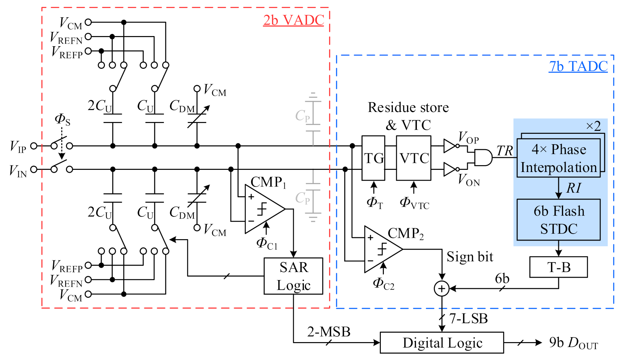
2.1. Architecture
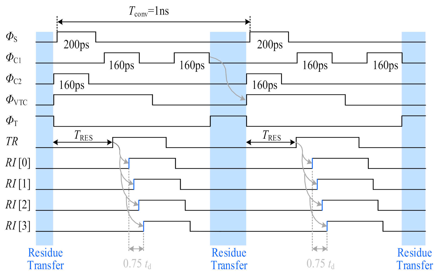
2.2. Timing
3. Circuit Implementation
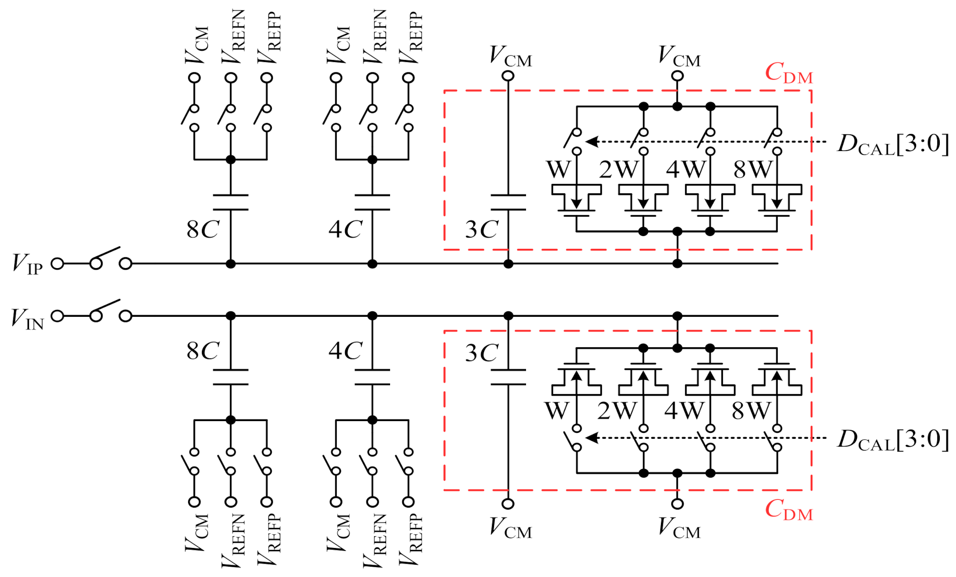
3.1. Capacitive DAC
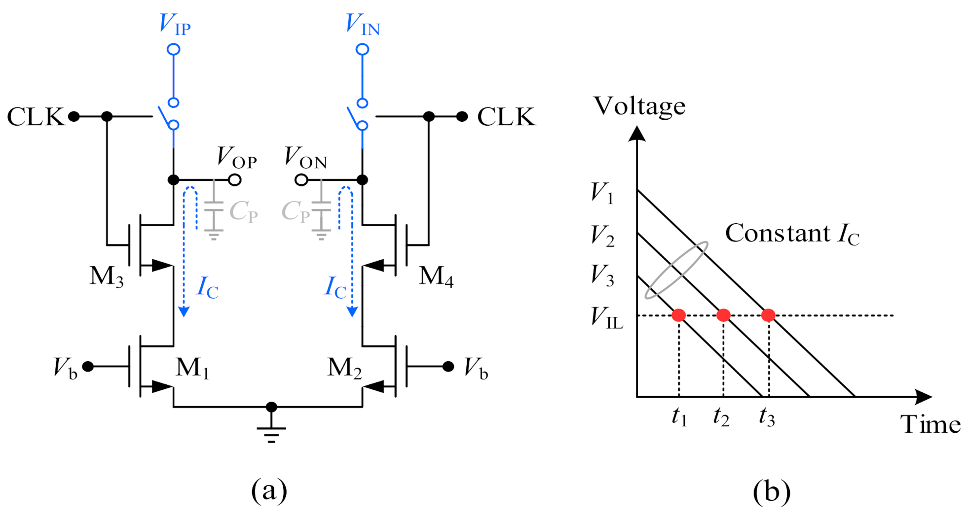
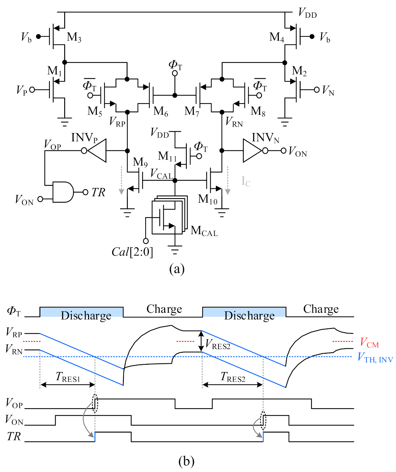
3.2. Voltage-to-Time Converter (VTC)
3.3. 6-Bit TDC
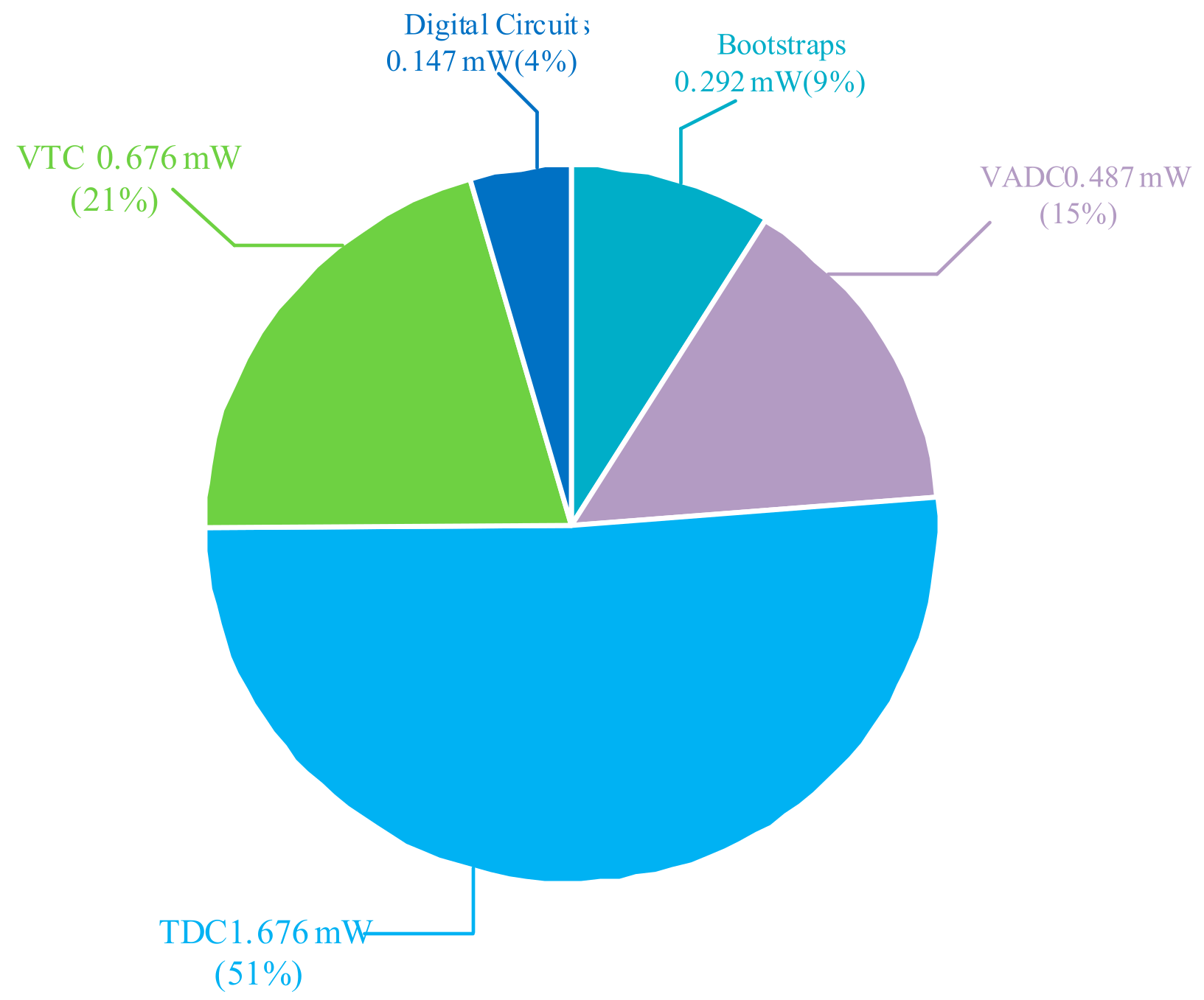
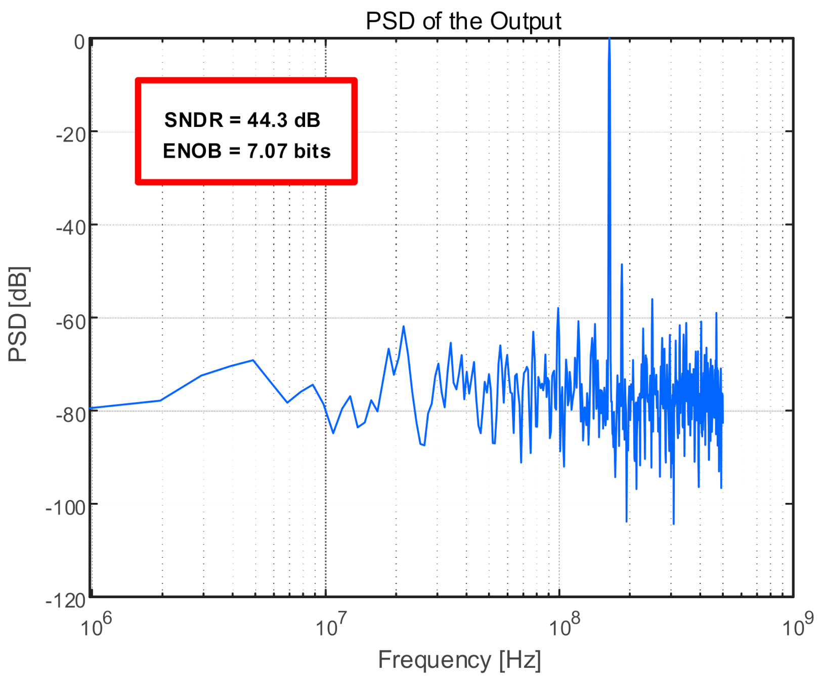
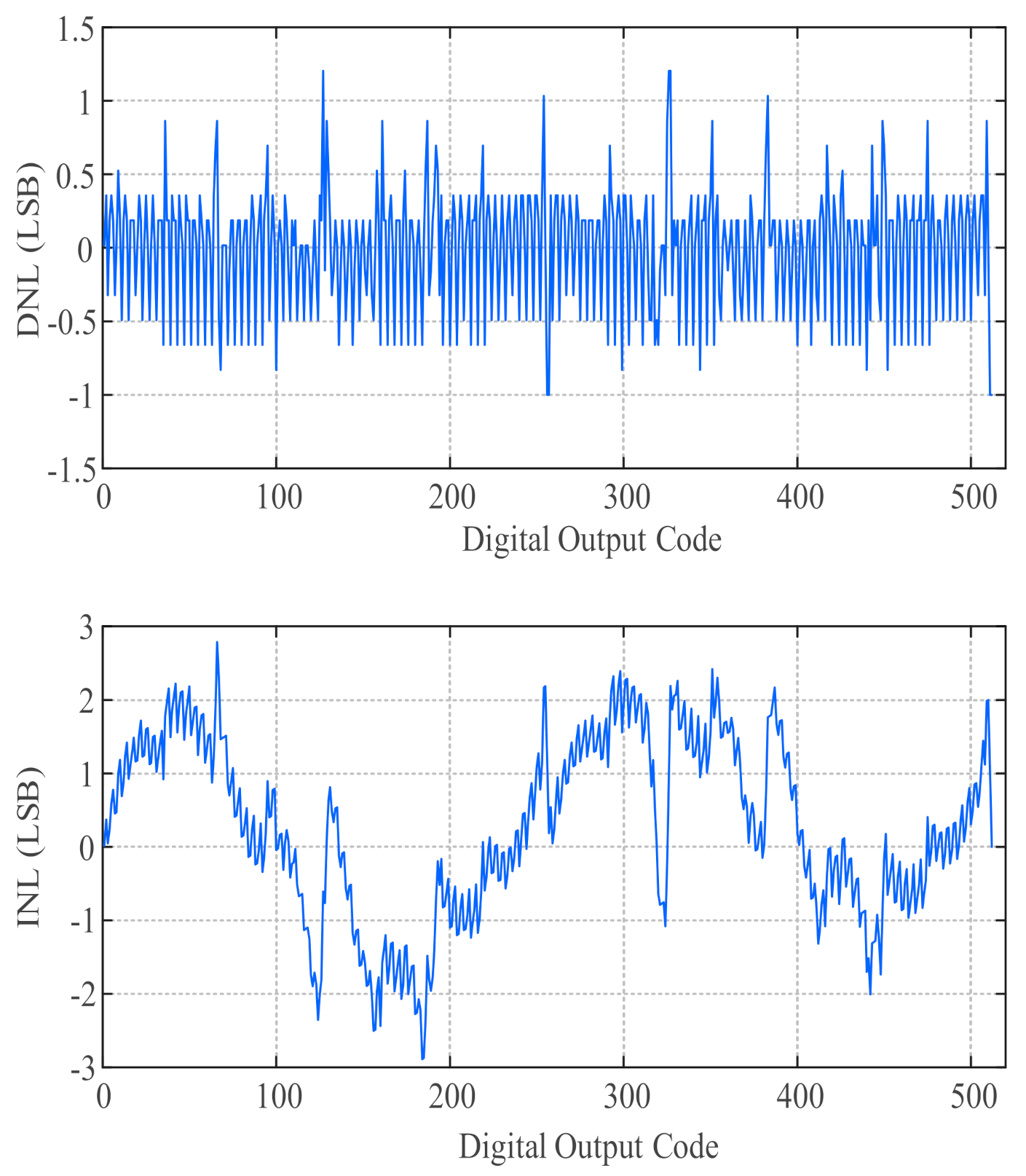
4. Experimental Results
5. Conclusions
Author Contributions
Funding
Data Availability Statement
Conflicts of Interest
References
- Kull, L.; Luu, D.; Menolfi, C.; Braendli, M.; Francese, P.A.; Morf, T.; Kossel, M.; Cevrero, A.; Ozkaya, I.; Toifl, T. A 24-to-72GS/s 8b time-interleaved SAR ADC with 2.0-to-3.3pJ/conversion and >30dB SNDR at nyquist in 14nm CMOS FinFET. In Proceedings of the 2018 IEEE Symposium on VLSI Circuits, Honolulu, HI, USA, 18–22 June 2018; pp. 358–360. [Google Scholar] [CrossRef]
- Keane, J.P.; Guilar, N.J.; Stepanovic, D.; Wuppermann, B.; Wu, C.; Tsang, C.W.; Neff, R.; Nishimura, K. 16.5 An 8GS/s time-interleaved SAR ADC with unresolved decision detection achieving −58dBFS noise and 4GHz bandwidth in 28nm CMOS. In Proceedings of the 2017 IEEE International Solid-State Circuits Conference (ISSCC), San Francisco, CA, USA, 5–9 February 2017; pp. 284–285. [Google Scholar] [CrossRef]
- Zhu, Y.; Chan, C.-H.; Martins, R. An 11b 1GS/s Time-Interleaved ADC with Linearity Enhanced T/H. In Proceedings of the 2018 IEEE Asian Solid-State Circuits Conference (A-SSCC), Tainan, Taiwan, 5–7 November 2018; pp. 1–2. [Google Scholar] [CrossRef]
- Chen, Y.; Wang, J.; Hu, H.; Ye, F.; Ren, J. A Time-Interleaved SAR Assisted Pipeline ADC With a Bias-Enhanced Ring Amplifier. IEEE Trans. Circuits Syst. II Express Briefs 2017, 65, 1584–1588. [Google Scholar] [CrossRef]
- Chen, Y.; Ni, Z.; Cao, Y.; Ye, F.; Ren, J. A 800 MS/s, 12-Bit, Ringamp-Based SAR assisted Pipeline ADC with Gain Error Cancellation. In Proceedings of the 2018 IEEE International Symposium on Circuits and Systems (ISCAS), Florence, Italy, 27–30 May 2018; pp. 1–4. [Google Scholar] [CrossRef]
- Muhlestein, J.; Leuenberger, S.; Sun, H.; Xu, Y.; Moon, U.-K. A 73dB SNDR 20MS/s 1.28mW SAR-TDC using hybrid two-step quantization. In Proceedings of the 2017 IEEE Custom Integrated Circuits Conference (CICC), Austin, TX, USA, 30 April–3 May 2017; pp. 1–4. [Google Scholar] [CrossRef]
- Su, Z.; Wang, H.; Zhao, H.; Chen, Z.; Wang, Y.; Dai, F.F. A 280MS/s 12b SAR-Assisted Hybrid ADC with Time Domain Sub-Range Quantizer in 45nm CMOS. In Proceedings of the 2019 IEEE Custom Integrated Circuits Conference (CICC), Austin, TX, USA, 14–17 April 2019; pp. 1–4. [Google Scholar] [CrossRef]
- Zhang, M.; Chan, C.-H.; Zhu, Y.; Martins, R.P. 3.5 A 0.6V 13b 20MS/s Two-Step TDC-Assisted SAR ADC with PVT Tracking and Speed-Enhanced Techniques. IEEE 2019, 66–68. [Google Scholar] [CrossRef]
- Liu, C.-C. 27.4 A 0.35mW 12b 100MS/s SAR-assisted digital slope ADC in 28nm CMOS. In Proceedings of the 2016 IEEE International Solid-State Circuits Conference (ISSCC), San Francisco, CA, USA, 31 January–4 February 2016; pp. 462–463. [Google Scholar] [CrossRef]
- Ramkaj, A.T.; Strackx, M.; Steyaert, M.S.J.; Tavernier, F. A 1.25-GS/s 7-b SAR ADC With 36.4-dB SNDR at 5 GHz Using Switch-Bootstrapping, USPC DAC and Triple-Tail Comparator in 28-nm CMOS. IEEE J. Solid-State Circuits 2018, 53, 1889–1901. [Google Scholar] [CrossRef]
- Lyu, Y. A 4-GS/s 39.9-dB SNDR 11.7-mW Hybrid Voltage-Time Two-Step ADC With Feedforward Ring Oscilla-tor-Based TDCs. IEEE JSSC 2020, 55, 1807–1818. [Google Scholar]


| ISSCC17 [2] Measured | A-SSCC18 [3] Measured | ISCAS18 [5] Simulated | This Work Simulated | |
|---|---|---|---|---|
| Type | TI-SAR | TI-pip-SAR | Pip-SAR | SAR-TDC |
| CMOS (nm) | 65 | 65 | 28 | 65 |
| Active Area (mm2) | 1.7 | 0.128 | 0.175 | 0.038 |
| Supply Voltage (V) | 1.2 | 1.2/2.5 | 1 | 1 |
| Power (mW) | 44.6 | 22 | 16.02 | 3.277 |
| Sampling Rate (GS/s) | 2.8 | 1 | 0.8 | 1 |
| SNDR (dB) | 48.2 | 54.3 | 60.9 | 44.3 |
| FoMwalden[fJ/c-s] | 75.8 | 43.7 | 22.5 | 24.3 |
Publisher’s Note: MDPI stays neutral with regard to jurisdictional claims in published maps and institutional affiliations. |
© 2021 by the authors. Licensee MDPI, Basel, Switzerland. This article is an open access article distributed under the terms and conditions of the Creative Commons Attribution (CC BY) license (https://creativecommons.org/licenses/by/4.0/).
Share and Cite
Bai, S.; Wan, Z.; Wan, P.; Zhang, H.; Ma, Y.; Zhang, X.; Liu, X.; Chen, Z. A 9-Bit 1-GS/s Hybrid-Domain Pseudo-Pipelined SAR ADC Based on Variable Gain VTC and Segmented TDC. Electronics 2021, 10, 2650. https://doi.org/10.3390/electronics10212650
Bai S, Wan Z, Wan P, Zhang H, Ma Y, Zhang X, Liu X, Chen Z. A 9-Bit 1-GS/s Hybrid-Domain Pseudo-Pipelined SAR ADC Based on Variable Gain VTC and Segmented TDC. Electronics. 2021; 10(21):2650. https://doi.org/10.3390/electronics10212650
Chicago/Turabian StyleBai, Suping, Zhi Wan, Peiyuan Wan, Hongda Zhang, Yongkuo Ma, Xiaoyu Zhang, Xu Liu, and Zhijie Chen. 2021. "A 9-Bit 1-GS/s Hybrid-Domain Pseudo-Pipelined SAR ADC Based on Variable Gain VTC and Segmented TDC" Electronics 10, no. 21: 2650. https://doi.org/10.3390/electronics10212650