Article

A 40-nm CMOS Piezoelectric Energy Harvesting IC for Wearable Biomedical Applications

1
Department of Electrical Engineering, National Sun Yat-Sen University, Kaohsiung 80424, Taiwan
2
Institute of Undersea Technology, National Sun Yat-Sen University, Kaohsiung 80424, Taiwan
3
Electrical and Electronics Engineering Institute, University of the Philippines Diliman, Quezon City 1101, Philippines
4
Department of Mechanical and Electro-Mechanical Engineering, National Sun Yat-Sen University, Kaohsiung 80424, Taiwan
5
Department of Electronic Engineering, National Yunlin University of Science and Technology, Yunlin 64002, Taiwan
*
Author to whom correspondence should be addressed.
Electronics 2021, 10(6), 649; https://doi.org/10.3390/electronics10060649
Submission received: 22 January 2021 / Revised: 4 March 2021 / Accepted: 8 March 2021 / Published: 11 March 2021

Abstract

:
This investigation presents an energy harvesting IC (integrated circuit) for piezoelectric materials as a substitute for battery of a wearable biomedical device. It employs a voltage multiplier as first stage which uses water bucket fountain approach to boost the very low voltage generated by the piezoelectric. The boosted voltage was further improved by the boost DC/DC converter which follows a predefined timing control directed by the digital logic for the said converter to be operated efficiently. TSMC 40-nm CMOS process was used for implementation and fabrication of the energy harvesting IC. The chip’s core has an area of 0.013 mm2. With an output of 1 V which is enough to supply the wearable biomedical devices, it exhibited the highest pump gain and accommodated the lowest piezoelectric generated voltage among recent related works.

1. Introduction

There is a huge demand for wearable sensors which are mainly used in monitoring health status of patients. Conventional batteries which are utilized as power supplies of these wearable sensors are being replaced. They may leak when they are not properly handled or packaged causing danger to the person. In addition, they cannot supply these wearables consistently due to limited battery capacity and the recharging requirement [1]. Moreover, they occupy too much space and add weight to the wearable sensor platforms [2,3]. Hence, they make the person wearing them feel uncomfortable. As a substitute for batteries in wearable sensor platforms, energy harvesting is being sought as a possible solution in providing power to these wearable sensors.
Meanwhile, human movements like feet and leg motion (walking and running), finger motion (writing and typewriting), and muscle contractions (heart, lung, and muscles) can bring an ample amount of wasted energy which can be harvested and converted to electricity. These biomechanical motions are commonly harvested by piezoelectric, electromagnetic, and triboelectric technologies [4,5]. Among the three energy harvesting technologies, piezoelectric is the most widely used and researched. Through the mechanical deformation of a piezoelectric material, an electricity is generated [4,6,7]. Some of the advantages of piezoelectric energy harvesting over the two technologies are higher energy density and output voltage [4,8]. The most widely known applications which utilized piezoelectrics are implemented in shoes [5,9]. More energy is generated by the piezoelectric when this is placed in shoes due to the weight exerted by the user standing on it and the continuous activities made by the user by walking and running. However, the generated output voltage from the vibration of piezoelectric material is not enough to supply or drive an electronic system [10]. One advantage of piezoelectric is that they can be easily integrated and interfaced with electronic systems implemented in a chip for more enhanced energy harvesting; thus, output voltage is now boosted [4,8,11,12].
Many related works have been reported regarding piezoelectric energy harvesting ICs for typical and wearable biomedical applications. A 0.5-m piezoelectric energy harvester was developed for wireless temperature monitoring which is capable of interfacing with wearables or implants where their data can be transmitted through the Internet (Internet of Things or IoT) [13]. It operates at a minimum input voltage of 0.51 V but generates voltage of only 3 V. In [8], they used a 130-nm CMOS full-bridge rectifier as energy harvester since the the voltage drop across the full-bridge rectifier is lower than the traditional off-chip diode. The voltage conversion ratio or pump gain is 0.987 while the output power is 10.7 W. Meanwhile, a piezoelectric energy harvesting circuit was developed that serves as supply to the wearable cannula for infant respiratory monitoring [14]. It has a pump gain of 0.987 but a higher output power of 11.1 W. A buck-boost converter was used for an input voltage of 0.54 V amplitude [15]. Its generated output voltage and power are 3.3 V and 57 mW, respectively. A 0.18-m piezoelectric energy harvester for wireless sensor nodes was proposed [16], where its possible generated output power and voltage are 94 W and 1.8 V for an input voltage of 1 V. Lastly, a study in [17] presented a 0.5-m CMOS vibrational energy harvester that has a pump gain of 3 but only operates at a minimum input voltage of 1 V.
In this study, a piezoelectric made from polyvinylidene fluoride (PVDF) was used because it is flexible which makes it to be wearable, comfortable, and non-intrusive or unobtrusive [14] to the users than the brittle piezoelectric made from lead zirconate titanate (PZT) [18]. The said PVDF as shown in Figure 1 has a wire diameter of 10 m and wire length of 1 mm. It has a vibration frequency of 6.67 Hz and maximum output voltage of 45 mV. Its output voltage was increased to 120 mV through series connection of the fibers. It was placed on the insole of the shoe.
Based from the previous works presented, none of them have developed an energy harvesting circuit that can accommodate an input voltage below 0.5 V. Previously, we proposed a PVDF film-based energy harvesting circuit [3] for the detection of missing children and elderly using a Bluetooth low energy (BLE) transceiver which requires at least 1 V power supply. Post-layout simulations were made for the evaluation of the said energy harvesting circuit with no chip implementation, measurements, and theoretical analysis conducted. In this paper, an energy harvesting circuit for low voltage PVDF piezoelectric which accommodates at least 120 mV-amplitude input voltage was realized that can be utilized for wearable biomedical applications. TSMC 40-nm CMOS process was used for implementation and fabrication of the energy harvesting IC. The fabricated chip was embedded inside the heel of the shoe for testing. It generates a maximum voltage of 1 V which is enough to drive and supply low-power and low-voltage wearable sensor platforms and systems.

2. System Architecture of Energy Harvester

The piezoelectric energy harvesting circuit architecture for wearable biomedical applications is shown in Figure 2. It is composed of AC/DC Converter, Voltage Monitor, and DC/DC Converter, which will be presented in the following subsections.

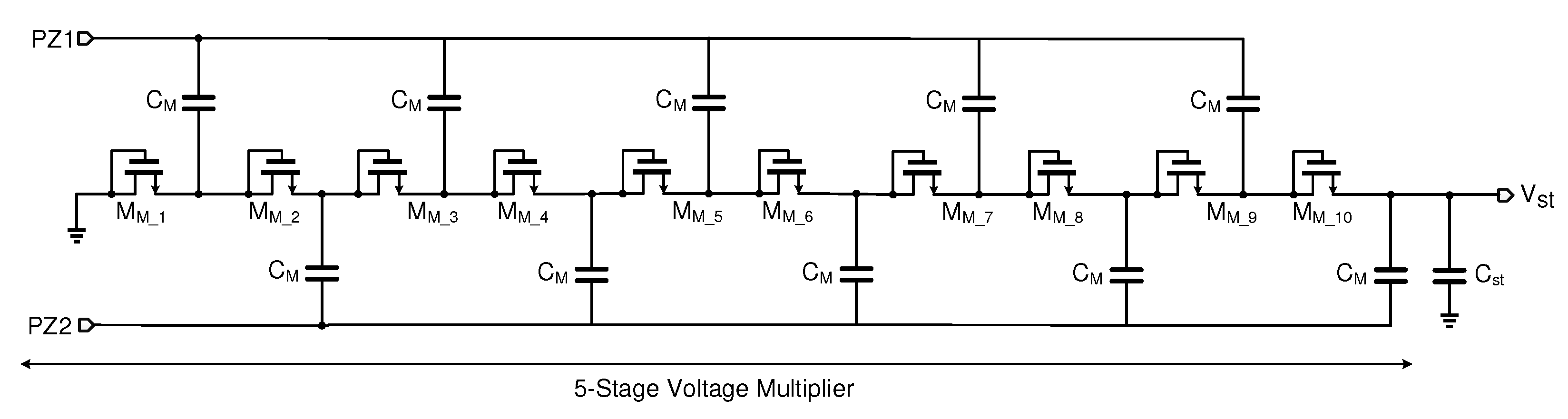
2.1. AC/DC Converter

In piezoelectric material energy harvesting circuits, AC/DC converters are needed. There are many different implementations for AC/DC converter circuits, e.g., [19]. However, due to efficiency and simplicity in practical applications of PVDF energy harvesting circuit for wearable biomedical devices, Voltage Multiplier or Charge Pump as shown in Figure 3 was selected in this study as AC/DC Converter in Figure 2. This 5-stage Voltage Multiplier is widely used in energy harvesting to convert AC to DC signals. It is a switched capacitor which elevates the lower voltage to a higher voltage value. Moreover, it can provide a preliminary boost to facilitate the design of the DC/DC Converter, thereby alleviating the problem of too small input voltage in the subsequent DC/DC Converter design. Because the PVDF film’s output voltages at PZ1 and PZ2 are very low, a low V t h transistor is utilized reducing the voltage drop and boosting the voltage efficiently.

2.2. Voltage Monitor

Since a very low output voltage is generated by the PVDF film, energy must be stored at Cst first. Then, the next stage will be driven by the large stored energy in Cst. As shown in Figure 4, Vst is monitored by a CMOS-based Schmitt trigger [20]. When Vst > high switching voltage VSPH, the power MOS switch Msw in Figure 2 is switched on. At this moment, the DC/DC converter is started by an enable signal (Vsw_n = 1). When Vst < low switching voltage VSPL, a disable signal is sent by the Schmitt trigger (Vsw_n = 0) to turn off the DC/DC converter and restore energy in Cst.

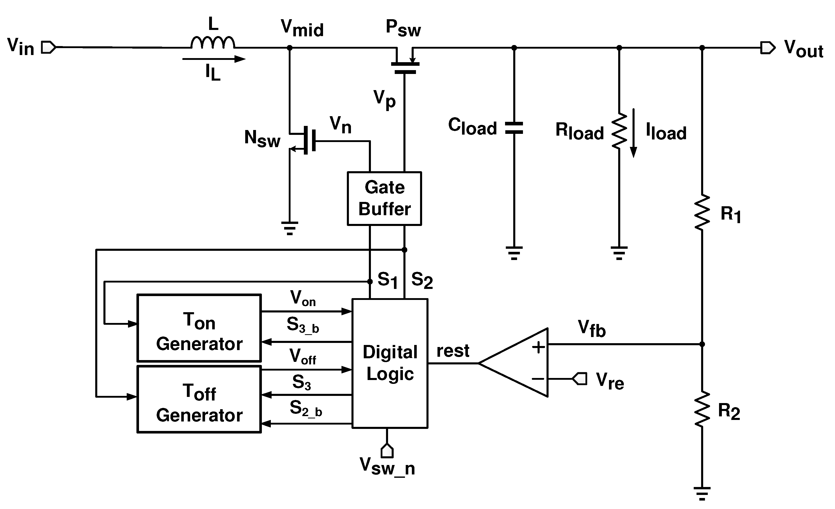
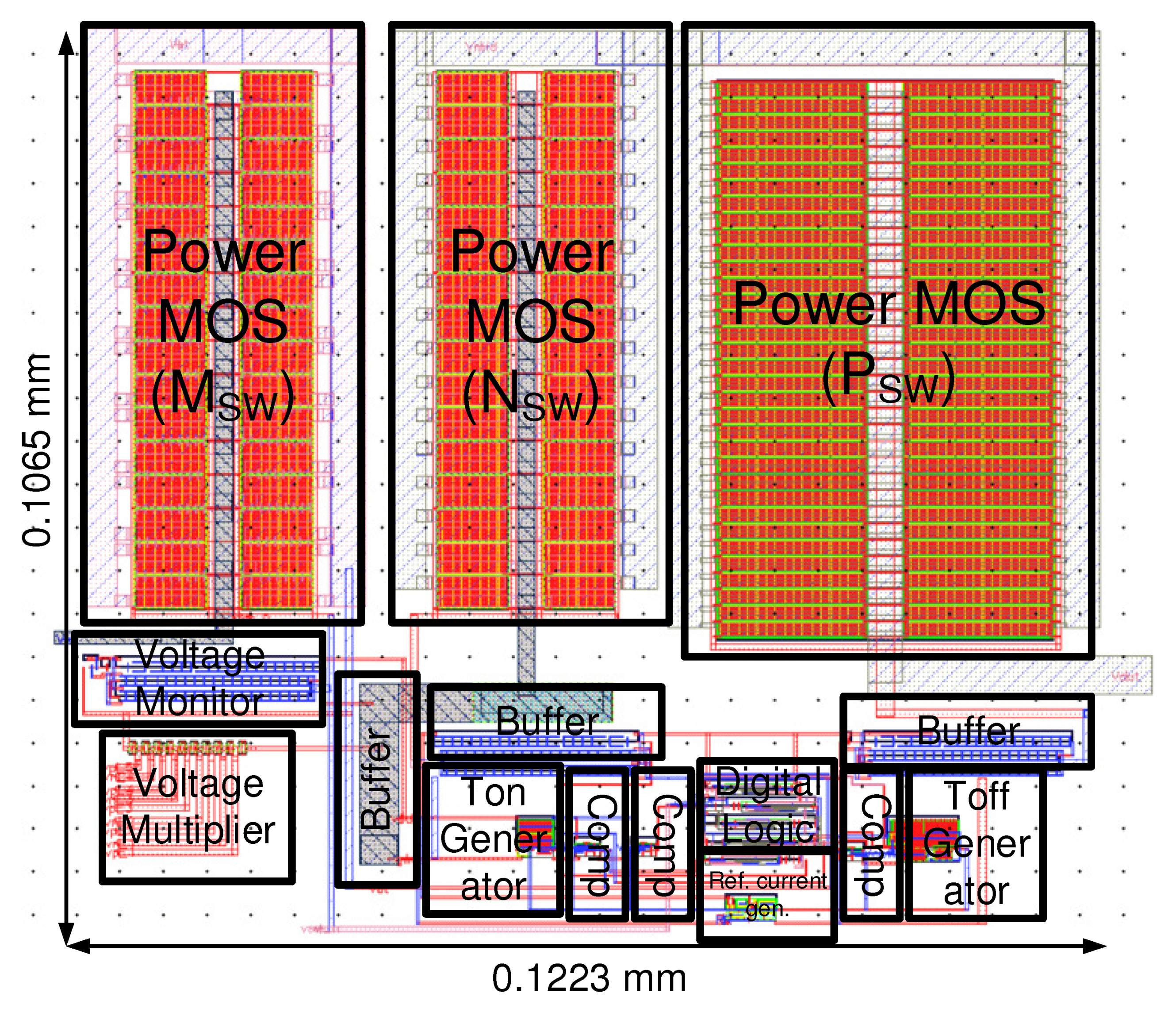
2.3. DC/DC Converter

The Boost DC/DC Converter is displayed in Figure 5 [21]. It is composed of Digital Logic, On-time Mode Generator (Ton Generator), Off-time Mode Generator (Toff Generator). The PMOS switch Psw is used to replace the diode which has lower voltage drop and better efficiency; hence, the said converter is a synchronous type instead of a diode architecture. Because of very low output voltage of PVDF, the bucket fountain method [22] is used in which the energy is kept in Cst until it is fully charged to the preset voltage value, and then the second stage boost is used to drive the wearable biomedical device. The Voltage Monitor is used to determine whether the stored voltage is sufficient. If the stored voltage is large enough, the power transistor (Msw) in Figure 2 is turned on, and a large enough voltage is generated through the DC/DC converter to drive the wearable biomedical device. The system is in standby state waiting for the next startup. When the Voltage Monitor sends an enable signal (Vsw_n = 1), the DC/DC converter will now start to operate. S1, S2, and S3 are generated by the Digital Logic. S 2 ¯ and S 3 ¯ are denoted by S2_b and S3_b, respectively. A comparator is interfaced to the Digital Logic for output adjustment.

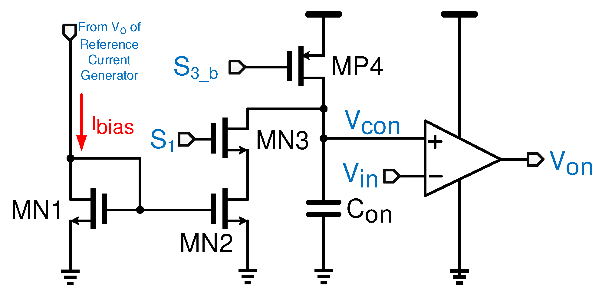
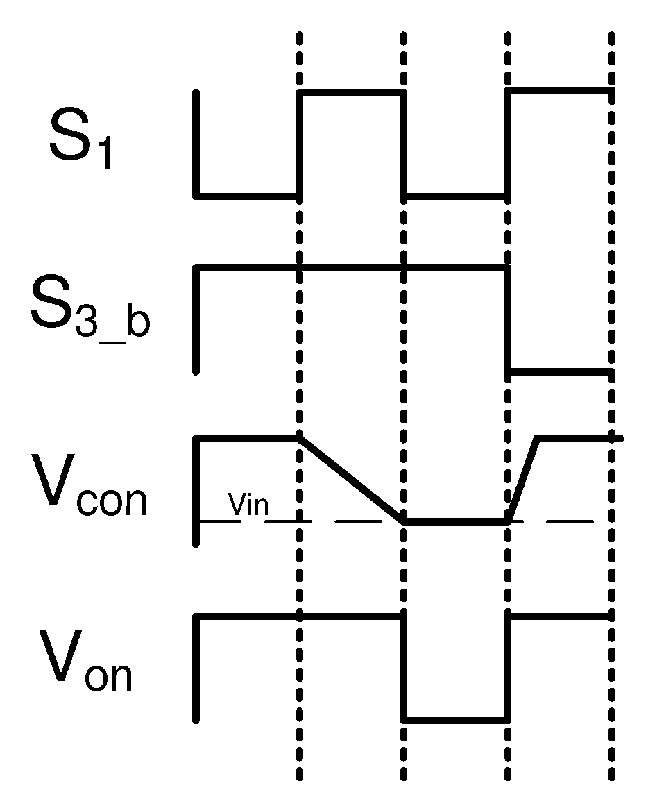
2.3.1. Ton Generator

The Ton Generator in Figure 5 is shown in Figure 6. It directs the Vn signal in Figure 5 to maintain the high pulse width (Vn = 1) which governs the ON time of the POWER NMOS Nsw. During Ton mode, S1 is high, S2 and S3 are low, MN3 is turned on while MP4 is at cutoff. A fixed current (Ion) discharges Con when Vcon < Vin is achieved. During Toff mode, S1 and S3 are low, S2 is high, and MN3 and MP4 are at cutoff prior to becoming equal values of Vcon and Vin. Figure 7 shows the timing diagram at Ton mode.

2.3.2. Toff Generator

The Toff generator in Figure 5 is shown in Figure 8. It directs the Vp signal to maintain the low pulse width (Vp = 1) for the ON time of power PMOS transistor Psw, and generates charging and discharging currents through the current mirror. During Ton mode where S1 is high, S2 and S3 are low, transistors MN7, MP10, and MN11 are at cutoff. On the contrary, during Toff mode, where S1 and S3 are low, S2 is high, MN11 is at cutoff while MN7 and MP10 are on. Therefore, this charges Coff with a fixed current until Vcoff > Vin is expected. Figure 9 shows the timing diagram at Toff mode.

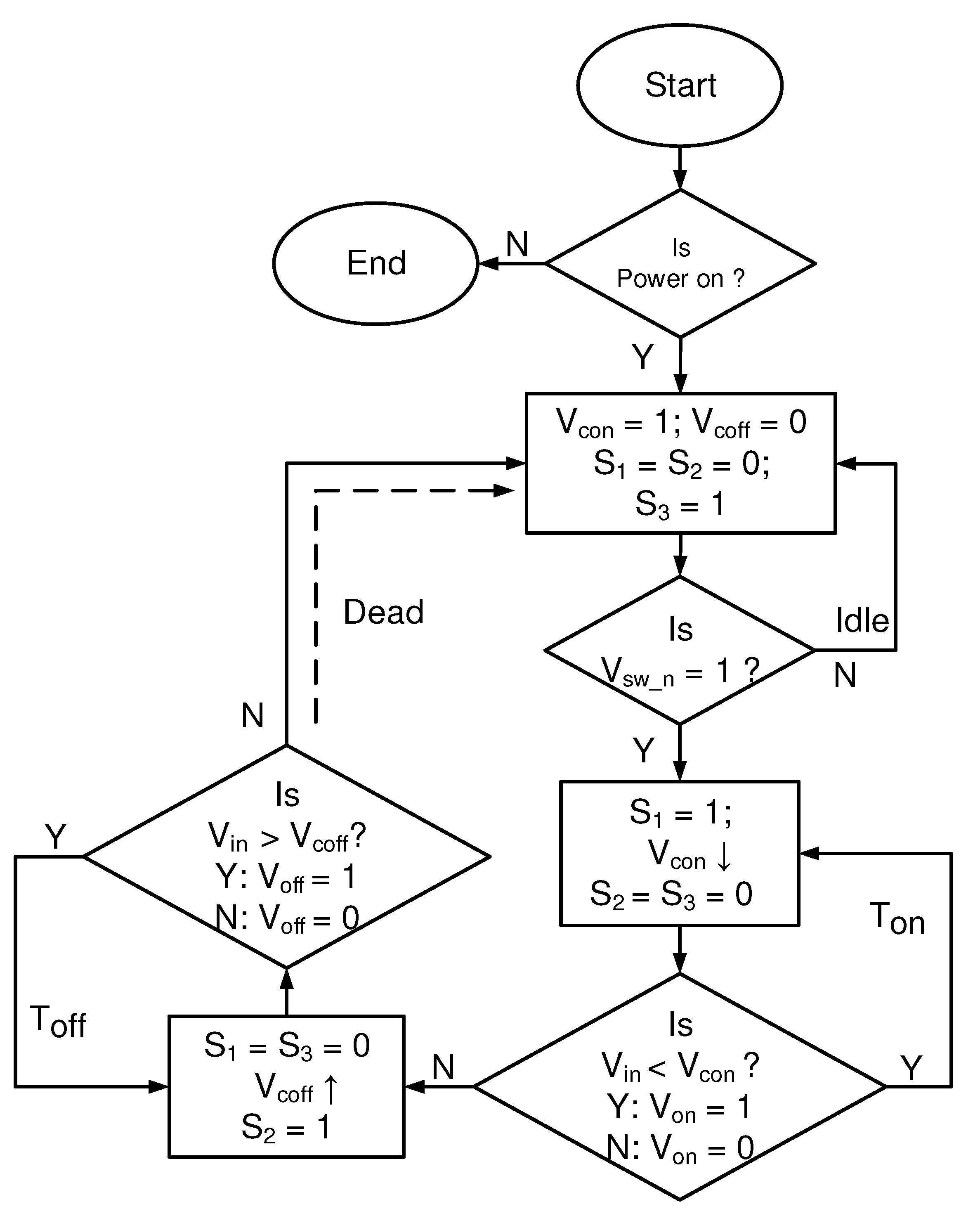
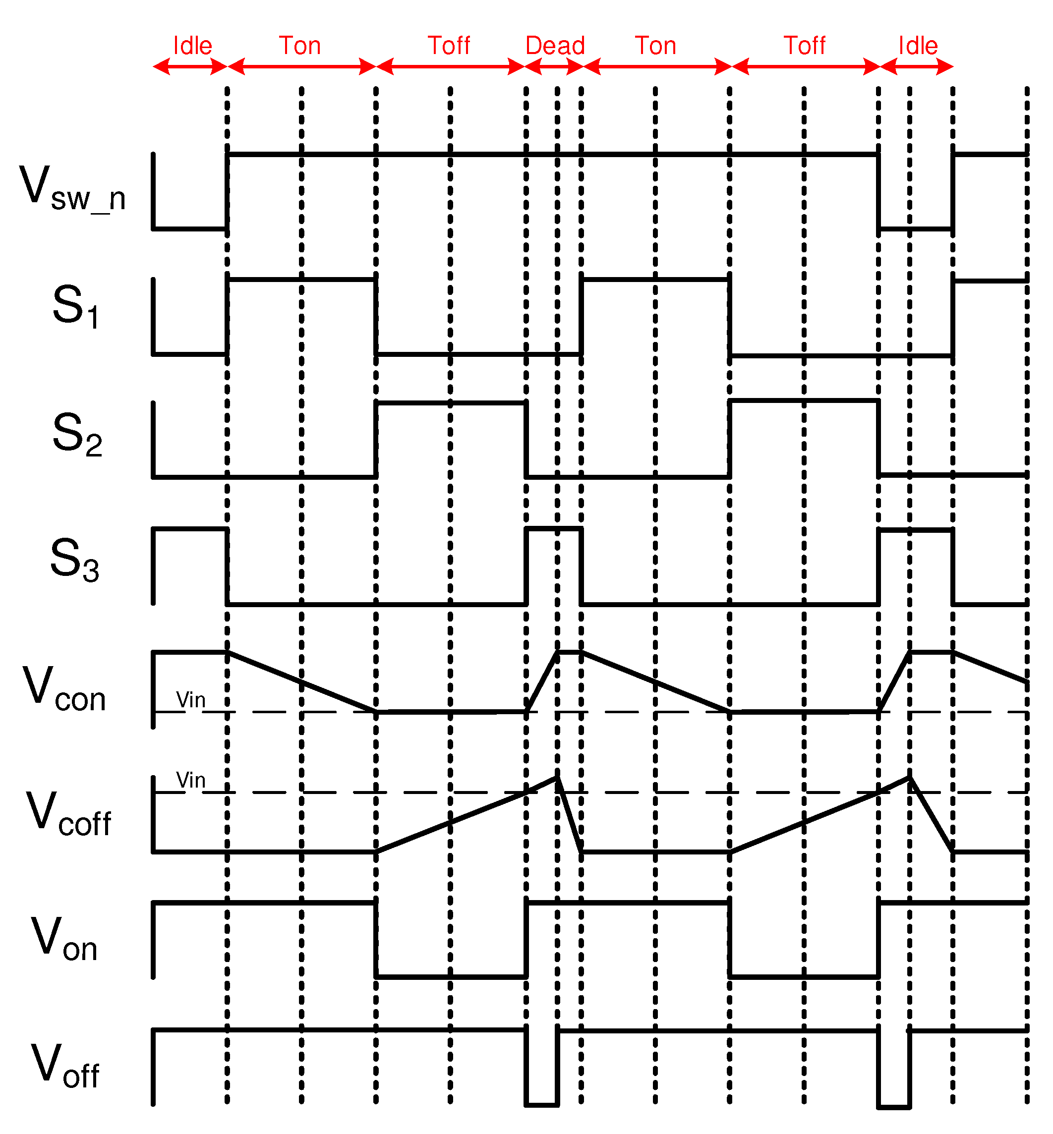
2.3.3. Digital Logic

Digital Logic in Figure 5 controls the signals’ timing sequence in the DC/DC converter, so that the DC/DC converter follows a predefined function for it to be operated correctly.
Figure 10 and Figure 11 show the flowchart and the timing diagram, respectively, of the timing control of Digital Logic in steady state. There are 3 modes: idle, on-time (Ton), and off-time (Toff). Looking at Figure 5 and Figure 10, the DC/DC converter starts at idle mode, and Digital Logic is at initial state when Vsw_n is low and S3 and Vcon are high.
The power MOS transistor (Msw) in Figure 2 will be on when a sufficiently high voltage is across Cst; thus, making Vsw_n high. When S1 which is connected to the Gate Buffer of Nsw and Vsw_n are high, and S2 which is connected to the Gate Buffer of Psw is low, the system enters Ton mode. At this time, the inductor L stores energy when IL flows through Nsw. The Ton generator controls the duration of the Ton mode. It will enable S1 to low after a predefined time when Vcon drops below Vin changing the system from Ton to Toff mode.
When S2 is high and S1 is low, the system enters Ton mode. Cload charges when (IL) flows through Psw. The Toff generator controls the duration of the Toff mode. It will enable S2 to low and S3 to high after a predefined time when Vin drops below Vcoff returning the system back from Toff to idle mode.

2.3.4. Reference Current Generator

Figure 12 shows the Reference Current Generator which provides a stable reference current (Ibias) needed in Figure 6 and Figure 8. The duty cycle contributed by the power switches (Nsw and Psw) depend on the Reference Current Generator. Since Ibias can be affected by power supply’s voltage and temperature variations, proportional (PTAT) and complementary to absolute temperature (CTAT) circuits are implemented to suppress the influence of temperature on accuracy and stability. In PTAT, both MN1 and MN2 are driven to subthreshold operation while both MP3 and MP4 are biased into strong inversion operation. PTAT current generator consists of transistors MN1, MN2, MP3, and MP4. Its generated Ipt0 is mirrored by MP3 and MP9 to the resulting (Ipt). Moreover, CTAT current generator is composed of MP5, MN6, MN7, and MP8. Its Int0 is mirrored by MP8 and MP9 to the output (Int). Then, the output current Ibias is the sum of Int and Ipt, which will be insensitive to temperature variations.

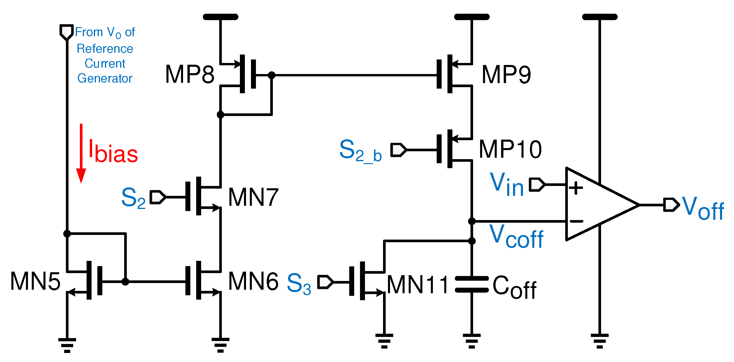
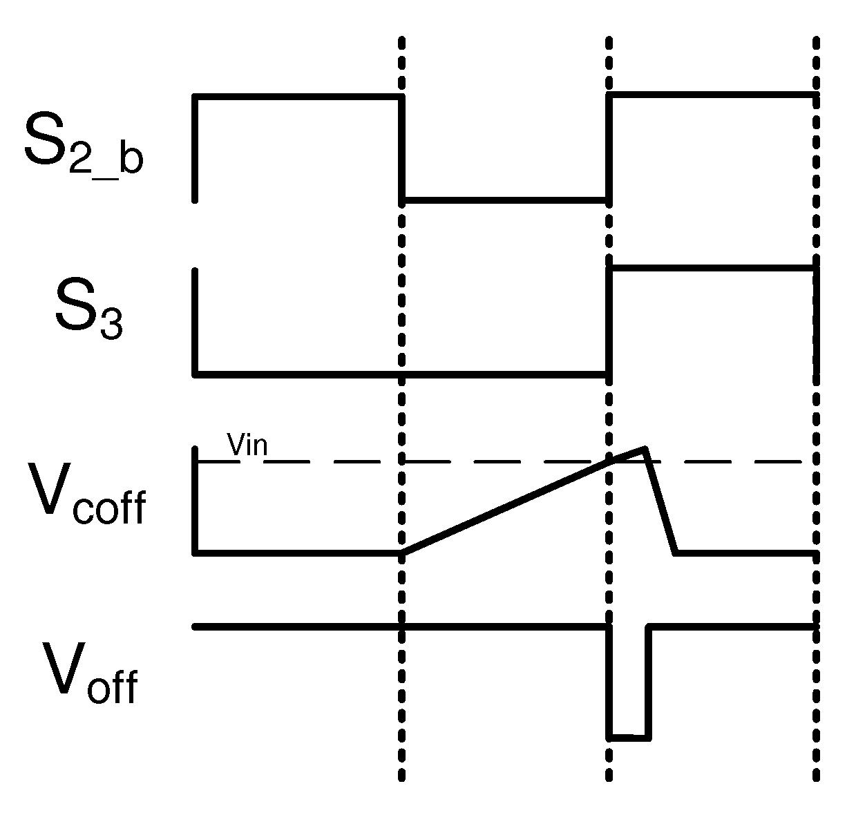
2.3.5. Comparator Circuit

The two comparators in the Ton and Toff Generators are used to regulate the on-time and off-time modes’ maintenance duration, respectively. For these two comparators, their propagation delay and noise have less effect to the their function and performance than the output-regulated Comparator in Figure 5. Therefore, the two comparators’ quiescent current can be fixed to a smaller value to consume less power. However, the trade-off is that the propagation delay will be larger. In this design, a two-stage open-loop comparator is used for the AC/DC converter’s output adjustment. It is shown in Figure 13.

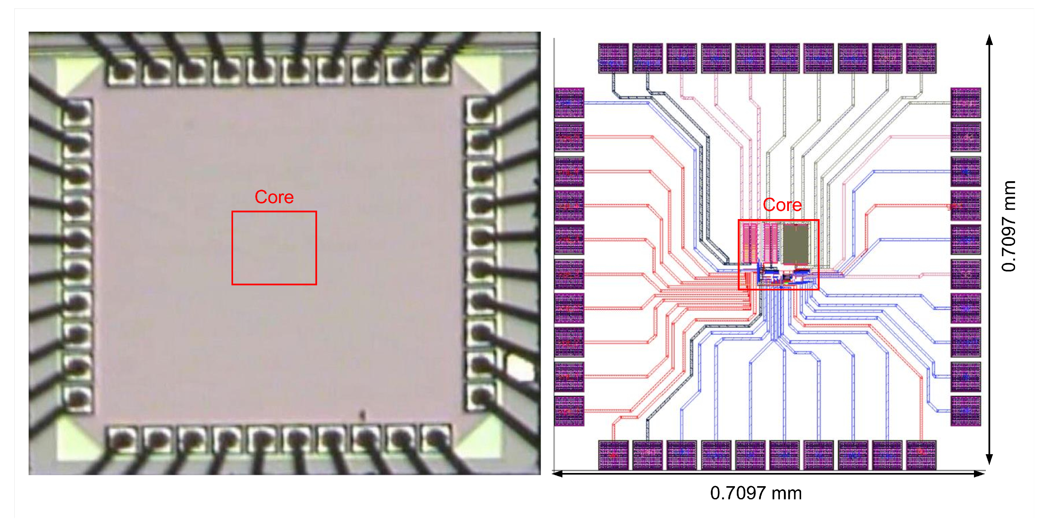
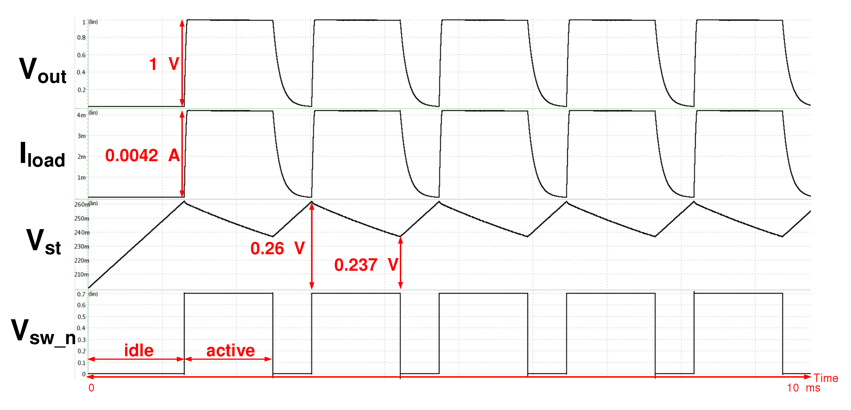
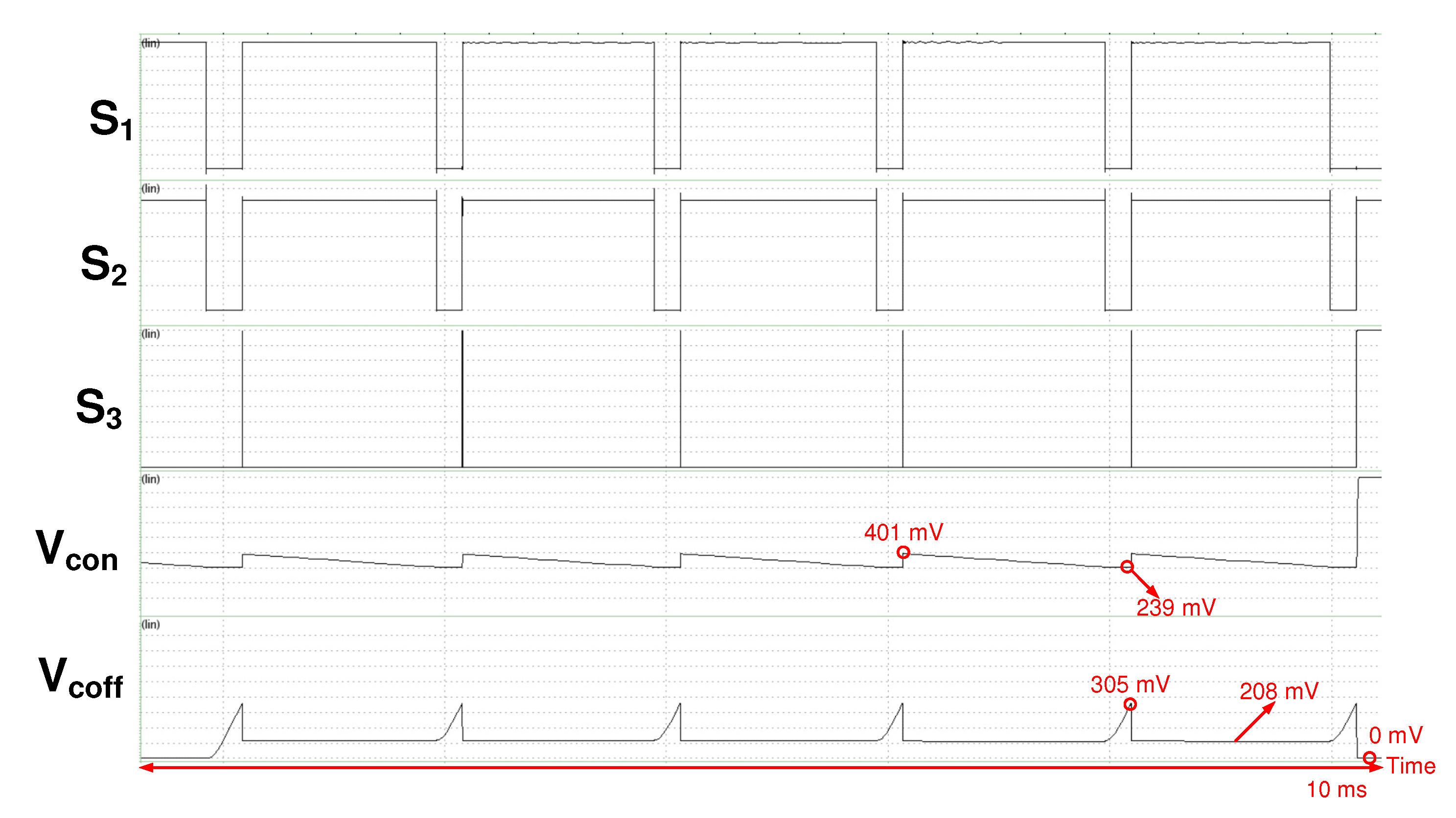
3. Measurement Results and Discussion

TSMC 40-nm CMOS process was used to implement and fabricate the PVDF piezoelectric energy harvesting IC. All of the transistor lengths are at minimum size. The aspect ratio of the width of the NMOS and PMOS transistors used in this chip is 2:1. The layout view of the core which has an area of 0.1223 × 0.1065 mm2 is shown in Figure 14 and Figure 15 and shows the die photo of the chip which has an area of 0.7097 × 0.7097 mm2. The core was covered by a dummy layer, as seen in the die photo, because there is a minimum metal density required by the foundry; hence, only the pads and the wire-bonds can be seen in the photo.
The fabricated chip was connected to PCB board and SMA connectors to reduce the loading effect. A power supply (ABM PRT3230 (ABM, Hsinchu City, Taiwan)) was used to provide VDD (0.9 V) and GND. A signal generator (Tektronix AFG3252 (Tektronix, Johnston, OH, USA))provides input signals for testing. It generates a 120 mV-amplitude sinusoid which mimics the excitation and the output voltage of the PVDF film for easy testing and validation of the proposed energy harvesting circuit. An oscilloscope (Teledyne Lecroy Waverunner 610Zi (Teledyne Lecroy, Thousand Oaks, CA, USA))observed the input and output waveforms. It was also used for the measurement and characterization of the PVDF film’s output voltage.
The output signal generated by the PVDF film, Vst, and Vsw_n signals are shown in Figure 16. A maximum of 100 kHz was used as PVDF’s vibration frequency for this testing. From Figure 17, it is noted that at the beginning the capacitor (Cst) was charged at 260 mV. When Vst reaches at least 260 mV, the Voltage Monitor sends an enable signal (Vsw_n = 1 V) to the DC/DC Converter to start the second mode of boosting which is the Ton mode.
Figure 18 summarizes the output specifications. The output voltage, current, and power are 1 V, 4.2 mA, and 4.2 mW, respectively. When the on-voltage value (Von) is lower than Vst (237 mV), Vsw_n is 0 then wait for the next enable signal. The resulting waveforms of the digital logic timing control in steady state is shown in Figure 18. It is consistent with the designed Digital Logic’s timing control waveforms in Figure 19.
Figure 20 shows the waveform of the output voltage Vout generated by the piezoelectric energy harvesting IC which is 1 V. For the PVDF generated voltage of 120 mV to 1 V, a regulated output voltage of 1 V is expected. The developed piezoelectric energy harvesting IC can be operated with a PVDF’s vibration frequency of 6.67 Hz to 100 kHz. The measurement results correspond with the post-layout simulation results made in the prior work [3]. With this, it can provide a stable power supply to the low-power and low-voltage wearable biomedical devices. The proposed piezoelectric energy harvesting IC is compared with the prior studies as shown in Table 1. In Table 1, it should be noted that the pump gain is represented as the ratio of Vout and the PVDF generated voltage. As shown in Table 1, the largest pump gain was generated by the proposed piezoelectric energy harvester IC over all the prior energy harvesting circuits cited in the literature.

4. Conclusions

A 40-nm CMOS piezoelectric energy harvesting IC has been presented. A Voltage Multiplier was constructed alleviating the problem of very low input voltage from the PVDF piezoelectric by boosting this low voltage. DC/DC converter improves the boosted voltage by following the Digital Logic’s predefined timing of three operating modes, namely, idle, Ton, and Toff. With this, the low-power, low-voltage wearable biomedical devices, which normally require 1 V as their supply, can be operated at stable condition by the developed piezoelectric energy harvesting IC. Among the prior studies, the proposed energy harvesting IC exhibited the highest pump gain and accommodated the lowest piezoelectric generated voltage.

Author Contributions

Conceptualization, C.-C.W., L.K.S.T., P.-C.C., and J.R.E.H.; methodology, C.-C.W., L.K.S.T., P.-C.C., C.-K.Y., C.-T.P., and Y.-H.H.; software, P.-C.C.; validation, L.K.S.T. and P.-C.C.; formal analysis, L.K.S.T. and P.-C.C.; investigation, L.K.S.T. and P.-C.C.; resources, C.-C.W., C.-K.Y., and C.-T. P.; data curation, L.K.S.T. and P.-C.C.; writing—original draft preparation, C.-C.W., L.K.S.T., and P.-C.C.; writing—review and editing, C.-C.W., L.K.S.T., J.R.E.H., and Y.-H.H.; visualization, P.-C.C.; supervision, C.-C.W.; project administration, C.-C.W.; funding acquisition, C.-C.W. All authors have read and agreed to the published version of the manuscript.

Funding

This research was funded by Ministry of Science and Technology (MOST), Taiwan, under grant MOST 109-2218-E-110-007- and 109-2224-E-110-001-.

Acknowledgments

The authors thank Taiwan Semiconductor Research Institute (TSRI) for the EDA tool assistance and chip fabrication.

Conflicts of Interest

The authors declare no conflict of interest.

References

  1. Mahmood, M.F.; Mohammed, S.L.; Gharghan, S.K. Free Battery-based Energy Harvesting Techniques for Medical Devices. IOP Conf. Ser. Mater. Sci. Eng. 2020, 745, 1–17. [Google Scholar] [CrossRef]
  2. Aroganam, G.; Manivannan, N.; Harrison, D. Review on wearable technology sensors used in consumer sport applications. Sensors 2019, 19, 1983. [Google Scholar] [CrossRef] [PubMed] [Green Version]
  3. Wang, C.-C.; Chen, P.-C.; Hsueh, Y.-H.; Pan, C.-T.; Yen, C.-K.; Lee, T.-J.; Hizon, J.R. A PVDF-film energy harvesting circuit using 40-nm CMOS process. In Proceedings of the 2020 2nd International Conference on Smart Power & Internet Energy Systems (SPIES), Bangkok, Thailand, 15–18 September 2020. [Google Scholar]
  4. Khalid, S.; Raouf, I.; Khan, A.; Kim, N.; Kim, H.S. A Review of Human-Powered Energy Harvesting for Smart Electronics: Recent Progress and Challenges. Int. J. Precis. Eng. Manuf.-Green Technol. 2019, 6, 821–851. [Google Scholar] [CrossRef]
  5. Iqbal, M.; Nauman, M.M.; Khan, F.U.; Abas, P.E.; Cheok, Q.; Iqbal, A.; Aissa, B. Multimodal Hybrid Piezoelectric-Electromagnetic Insole Energy Harvester Using PVDF Generators. Electronics 2020, 9, 635. [Google Scholar] [CrossRef] [Green Version]
  6. Jeong, S.Y.; Cho, J.Y.; Hong, S.D.; Hwang, W.; Jabbar, H.; Ahn, J.H.; Jhun, J.P.; Sung, T.H. Self-Powered Operational Amplifying System with a Bipolar Voltage Generator Using a Piezoelectric Energy Harvester. Electronics 2020, 9, 41. [Google Scholar] [CrossRef] [Green Version]
  7. Fernandez, E.O.; Gobres, E.R.; Thio-ac, A.C.; Jandumon, M.S.; Ong, C.L.G.; Perez, R.B.; Ramos, P.G. Design Optimization of Low Power Wind Belt Electric Generator using Piezoelectric Transducer. In Proceedings of the 2018 IEEE 10th International Conference on Humanoid, Nanotechnology, Information Technology, Communication and Control, Environment and Management (HNICEM), Baguio City, Philippines, 29 November–2 December 2018. [Google Scholar]
  8. Oh, T.; Islam, S.K.; Mahfouz, M.; To, G. A Low-Power CMOS Piezoelectric Transducer Based Energy Harvesting Circuit for Wearable Sensors for Medical Applications. J. Low Power Electron. Appl. 2017, 7, 33. [Google Scholar] [CrossRef] [Green Version]
  9. Zhao, J.; You, Z. A Shoe-Embedded Piezoelectric Energy Harvester for Wearable Sensors. Sensors 2014, 14, 12497–12510. [Google Scholar] [CrossRef] [PubMed]
  10. Cepenas, M.; Peng, B.; Andriukaitis, D.; Ravikumar, C.; Markevicius, V.; Dubauskiene, N.; Navikas, D.; Valinevicius, A.; Zilys, M.; Merfeldas, A.; et al. Research of PVDF Energy Harvester Cantilever Parameters for Experimental Model Realization. Electronics 2020, 9, 2030. [Google Scholar] [CrossRef]
  11. Caliò, R.; Rongala, U.B.; Camboni, D.; Milazzo, M.; Stefanini, C.; De Petris, G.; Oddo, C.M. Piezoelectric Energy Harvesting Solutions. Sensors 2014, 14, 4755–4790. [Google Scholar] [CrossRef] [PubMed] [Green Version]
  12. Pillatsch, P.; Yeatman, E.M.; Holmes, A.S.; Wright, P.K. Wireless power transfer system for a human motion energy harvester. Sens. Actuators A Phys. 2016, 244, 77–85. [Google Scholar] [CrossRef] [Green Version]
  13. Fan, S.; Zheng, X.-Q.; Wei, R.; Pulskamp, J.S.; Rudy, R.; Polcawich, R.G.; Feng, P.X.-L. mm-scale and MEMS piezoelectric energy harvesters powering on-chip cmos temperature sensing for IoT applications. In Proceedings of the IEEE 2017 19th International Conference on Solid-State Sensors, Actuators and Microsystems (TRANSDUCERS), Kaohsiung, Taiwan, 18–22 June 2017. [Google Scholar]
  14. Mahbub, I.; Oh, T.; Shamsir, S.; Islam, S.K.; Pullano, S.A.; Fiorillo, A.S. Design of a pyroelectric charge amplifier and a piezoelectric energy harvester for a novel non-invasive wearable and self-powered respiratory monitoring system. In Proceedings of the 2017 IEEE Region 10 Humanitarian Technology Conference (R10-HTC), Dhaka, Bangladesh, 21–23 December 2017. [Google Scholar]
  15. Mostafa, M.G.; Motakabber, S.M.A.; Ibrahimy, M.I. Design and analysis of a buck-boost converter circuit for piezoelectric energy harvesting system. In Proceedings of the 2016 International Conference on Computer and Communication Engineering (ICCCE), Kuala Lumpur, Malaysia, 26–27 July 2016. [Google Scholar]
  16. Aktakka, E.E.; Najafi, K. A micro inertial energy harvesting platform with self-supplied power management circuit for autonomous wireless sensor nodes. IEEE J. Solid State Circ. 2014, 49, 2017–2029. [Google Scholar] [CrossRef]
  17. Rao, Y.; Arnold, D.P. An input-powered vibrational energy harvesting interface circuit with zero standby power. IEEE Trans. Power Electron. 2011, 26, 3524–3533. [Google Scholar] [CrossRef]
  18. Vatansever, D.; Hadimani, R.L.; Shah, T.; Siores, E. An investigation of energy harvesting from renewable sources with PVDF and PZT. Smart Mater. Struct. 2011, 20, 1–6. [Google Scholar] [CrossRef]
  19. Weng, P.S.; Tang, H.Y.; Ku, P.C.; Lu, L.H. 50 mV-input batteryless boost converter for thermal energy harvesting. IEEE J. Solid State Circ. 2013, 48, 1031–1041. [Google Scholar] [CrossRef]
  20. Baker, R.J. CMOS: Circuit Design, Layout, and Simulation, 4th ed.; John Wiley & Sons: Hoboken, NJ, USA, 2019; pp. 523–528. [Google Scholar]
  21. Wang, J. Design of a Boost DC-DC Converter for Energy Harvesting Applications in 40 nm CMOS Process. Master’s Thesis, Delft University of Technology, Delft, The Netherlands, 2014. [Google Scholar]
  22. Teh, Y.K.; Mok, P.K. A piezoelectric energy harvesting interface circuit using one-shot pulse transformer boost converter based on water bucket fountain strategy. In Proceedings of the 2014 IEEE International Symposium on Circuits and Systems (ISCAS), Melbourne, Australia, 1–5 June 2014. [Google Scholar]
Figure 1. Polyvinylidene fluoride (PVDF) piezoelectric used in the proposed energy harvester.
Electronics 10 00649 g001
Figure 2. PVDF energy harvesting circuit.
Electronics 10 00649 g002
Figure 3. Voltage multiplier or charge pump as AC/DC converter.
Electronics 10 00649 g003
Figure 4. Schmitt trigger as voltage monitor.
Electronics 10 00649 g004
Figure 5. Boost DC/DC converter.
Electronics 10 00649 g005
Figure 6. Ton generator.
Electronics 10 00649 g006
Figure 7. Timing diagram at Ton mode.
Electronics 10 00649 g007
Figure 8. Toff generator.
Electronics 10 00649 g008
Figure 9. Timing diagram at Toff mode.
Electronics 10 00649 g009
Figure 10. Flowchart of the timing control of Digital Logic.
Electronics 10 00649 g010
Figure 11. Timing diagram of the timing control of Digital Logic.
Electronics 10 00649 g011
Figure 12. Reference current generator.
Electronics 10 00649 g012
Figure 13. Comparator schematic.
Electronics 10 00649 g013
Figure 14. Core layout view of the piezoelectric energy harvesting IC.
Electronics 10 00649 g014
Figure 15. Die photo of the piezoelectric energy harvesting IC.
Electronics 10 00649 g015
Figure 16. Waveforms of PVDF output signal, Vst, and Vsw_n.
Electronics 10 00649 g016
Figure 17. Waveform of the charging of capacitor Cst.
Electronics 10 00649 g017
Figure 18. Waveforms of Vout, Iload, Vst, and Vsw_n.
Electronics 10 00649 g018
Figure 19. Digital Logic’s timing control waveforms.
Electronics 10 00649 g019
Figure 20. Waveform of Vout.
Electronics 10 00649 g020
Table 1. Comparison of the piezoelectric energy harvesting circuit with prior studies.
[13][8][14][15][16][17]This work
Year2017201720172016201420112021
TypePZTVibrationalPVDFPiezoelectricPZTVibrationalPVDF
Process0.5 μm130 nm130 nmPSpice0.18 μm0.5 μm40 nm
PVDF voltage0.51 V0.704 V0.703 V0.54 V1 V1 V0.12 V
Vout3 V0.694 V0.694 V3.3 V1.8 V3 V1 V
PoutN.A.10.7 μW11.1 μW57 mW55 μW3.9 mW4.2 mW
Ripple40 mVN.A.N.A.N.A.N.A.N.A.3 mV
Pump gain5.880.9870.9876.111.8038.33
Publisher’s Note: MDPI stays neutral with regard to jurisdictional claims in published maps and institutional affiliations.

