
GateRL: Automated Circuit Design Framework of CMOS Logic Gates Using Reinforcement Learning


Department of Information Display, Kyung Hee University, Seoul 02447, Korea
*
Author to whom correspondence should be addressed.
Electronics 2021, 10(9), 1032; https://doi.org/10.3390/electronics10091032
Submission received: 5 April 2021
/
Revised: 22 April 2021
/
Accepted: 24 April 2021
/
Published: 26 April 2021
(This article belongs to the Special Issue Machine Learning in Electronic and Biomedical Engineering)
Abstract
:This paper proposes a GateRL that is an automated circuit design framework of CMOS logic gates based on reinforcement learning. Because there are constraints in the connection of circuit elements, the action masking scheme is employed. It also reduces the size of the action space leading to the improvement on the learning speed. The GateRL consists of an agent for the action and an environment for state, mask, and reward. State and reward are generated from a connection matrix that describes the current circuit configuration, and the mask is obtained from a masking matrix based on constraints and current connection matrix. The action is given rise to by the deep Q-network of 4 fully connected network layers in the agent. In particular, separate replay buffers are devised for success transitions and failure transitions to expedite the training process. The proposed network is trained with 2 inputs, 1 output, 2 NMOS transistors, and 2 PMOS transistors to design all the target logic gates, such as buffer, inverter, AND, OR, NAND, and NOR. Consequently, the GateRL outputs one-transistor buffer, two-transistor inverter, two-transistor AND, two-transistor OR, three-transistor NAND, and three-transistor NOR. The operations of these resultant logics are verified by the SPICE simulation.
1. Introduction
Over the past decade, machine learning (ML) algorithms, especially deep learning (DL) approaches, have attracted lots of interests in a variety of applications, such as image classification [1], object detection [2], image/video search [3], super resolution [4], language translation [5], speech recognition [6], stock market prediction [7], and so on, due to their dramatic advances, along with highly increased processing power and huge amount of training datasets [8].
Besides, there have also been many ML-related research studies on the field of the circuit design [9]. One direction is to implement ML networks in existing or specialized hardware platforms. While various simplification methods have been proposed to alleviate the requirement on processing power and data bandwidth [10,11,12], highly complicated and large size DL networks have been realized based on specialized integrated circuit solutions, such as tensor processing units (TPUs) [13] and general purposed graphics processing units (GPGPUs) [14] that enable the acceleration of DL computations. The other approach is to employ ML algorithms during the course of the integrated circuit design. ML methods optimize transistors’ sizes of a given circuit schematic in various points of view of target performances, including power consumption, bandwidth, gain, and area [15,16]. At the layout stage, MLs automate the placement procedure to avoid the routing errors in advance for the small chip area [17,18]. These approaches lead to the substantial reduction on the overall design time by the much smaller number of iterations in simulation and layout stages. In particular, a Berkeley analog generator (BAG) has been studied as the designer-oriented framework since 2013 [19,20]. BAG contains the whole circuit design procedures, including schematic, layout, and verification. Its schematic design platform selects one architecture for a given specification and optimizes parameters. The DL-based layout optimization for a BAG framework was also proposed in 2019 [21].
On the other hand, to the best of our knowledge, there have been no research results to devise DL to design the circuit structure from the scratch at the transistor level. These circuit structure generators cannot avoid very large hypothesis space because a transistor have three terminals of source, gate, and drain that can be connected to each other and used as input, output, or internal node. As a result, it is much more difficult to give rise to the custom schematic directly than to use given circuit blocks that have dedicated ports for inputs and outputs. This paper proposes an automated schematic design framework (GateRL) for digital logic gates, such as inverter, buffer, NAND, AND, NOR, and OR, at the backplane of complementary metal on semiconductor (CMOS) transistors. This full custom design scheme is required for special circuits in the situation with limitations, such as thin-film transistor (TFT) shift registers integrated in display panels, where only one-type TFTs are allowed [22,23,24,25]. While most off-the-shelf applications have been based on the supervised learning networks trained with a huge amount of data and labels, the GateRL employs the reinforcement learning (RL) [26] because the schematic design is difficult to provide labels and only whether the resultant circuit works or not can be decided. The remaining parts are organized as follows. In Section 2, the proposed GateRL is explained in detail by addressing overall architecture and variables exchanged between agent and environment. Section 3 demonstrates the experimental results that include the schematics proposed by the GateRL and their simulation results by simulation program with integrated circuit emphasis (SPICE). Section 4 concludes this paper.
2. Proposed GateRL Architecture
A proposed GateRL system is based on the RL methodology that consists of agent and environment, as shown in Figure 1. While the agent sends an action () to the environment to add a new connection to the schematic, the environment updates state (), reward (), and mask () and transfers them to the agent again. Unlike general RL networks, the GateRL makes use of the action masking scheme to take into account several constraints in the circuit design, as well as to reduce the size of the action space [27]. The target logic gate is specified by the truth table (T), where corresponding outputs are described over all the combinations of inputs.
2.1. State ()
is extracted from the connection matrix (CM) that is similar to an adjacency matrix of a graph theory [28]. As depicted in Figure 2, all possible nodes of the schematic are equally assigned to columns and rows of CM, leading to the shape of a square matrix. , , , and are the numbers of inputs, outputs, n-type MOS (NMOS) transistors, and p-type MOS (PMOS) transistors, respectively. Therefore, the total number of columns or rows () can be obtained by Equation (1). The first two columns and two rows represent connections to supply voltage sources of VDD and GND. In particular, because transistors have three terminals of source (S), gate (G), and drain (D), the numbers of their nodes are calculated by means of the product of the number of transistors and the factor of 3. The connections of their body terminals are omitted by assuming that bodies of all NMOS and PMOS transistors are fixed at GND and VDD, respectively. From here, the node assigned to the i-th row or column is addressed as the node i ().
An element of CM at i-th row and j-th column () is assigned to 0 or 1, where 0 means no connection, and 1 indicates the connection between two corresponding nodes as expressed in Equations (2) and (3). Therefore, the circuit schematic can be extracted from a given CM. For example, CM of Figure 3a is converted into the schematic of Figure 3b, where , , , and are 1, 1, 1, and 0. In addition, since all the connections in the circuit schematic are undirected, CM is constructed as a symmetric matrix.
In the connection of circuit elements, there exist constraints on CM. Firstly, direct connections between VDD, GND, inputs, and outputs must not be allowed to avoid shoot-through currents between voltages sources and to guarantee the functionality of outputs according to the combinations of inputs. Thus, the corresponding area of CM is always filled with 0. Secondly, the self-connections described by diagonal elements have no meaning in the circuit, leading to the diagonal elements () fixed at 0 all the time. Thirdly, as CM is a symmetric matrix, the full matrix can be reconstructed from the half area over the diagonal. As a result, the whole CM can be represented with the area marked in Figure 4 that is reshaped into in a form of a vector by flattening. Its length () is calculated as Equation (4) that is derived by dividing the region into a rectangular part and a triangular part.
2.2. Mask ()
In addition to three above constraints, the proposed algorithm defines two more constraints that can be applied during schematic design steps. The first one is that VDD, GND, and inputs should not be connected to each other through a single transistor. This connection causes the short circuit situation between voltage sources. Thus, any two nodes among them must not be connected to source and drain terminals of the same transistor, respectively. For example, whenever VDD is linked to the source of a transistor, GND and inputs cannot be placed at its drain. The second constraint is that the connection of a single signal to both source and drain of a transistor is not allowed. Because this connection can be replaced with a simple short circuit, that transistor is not necessary.
In the first place, a masking matrix (MM) is generated with respect to the current CM. MM is also the square matrix of where each element () of 0 or 1 represents whether that connection is available or not, respectively as described in Equation (5). Four masking criteria are reflected on MM as follows. First, since it is not necessary to repeat existing connections, corresponding elements of MM are set to be 1. Second, all direct connections between VDD, GND, inputs, and outputs are blocked. When a node is connected to one of VDD, GND, inputs, and outputs, that node must not be connected to any others of them. Therefore, elements of those short connections are also marked as 1 in MM. Third, when one of source and drain terminals is connected to VDD or GND or inputs, the other terminal of the same transistor must avoid the connection to VDD, GND, and inputs that brings about the drastic shoot-through currents between voltage sources via the transistor turned on. Fourth, it is forbidden to connect a single signal to both source and drain of a transistor. When one of source and drain is connected to a signal, its other terminal should not be assigned to the same signal.
From the second to the fourth, all possible connections via other nodes are simultaneously blocked. In the circuit, the connection of two nodes through different nodes is equal to their direct connection. Therefore, whenever is set to 1, it is checked out whether that corresponding i-th row and j-th column include multiple 1s at CM. If so, all connections between nodes linked to node i and node j are taken into account as the connected ones and then, corresponding elements of MM are set to 1. Finally, after MM is updated by processing four resultant matrixs through logical OR operation, is generated in a vector form, like , by flattening the upper right region of MM. The overall procedure of the mask generation is closely explained in Figure 5, where , , , and are 1, 1, 1, and 1.
2.3. Reward ()
Since the proposed GateRL simply defines as +1 for the correctly working schematic and −1 for others, it is expected that the GateRL proposes the working schematics with the minimum number of connection steps, that is, the minimum number of transistors. Therefore, it is of the most importance to verify whether the schematic represented by CM meets a given truth table or not. For example, the truth table of an inverter regarding CM of and consists of four rows that include combinations of two inputs (, ) and their target outputs () as illustrated in Figure 6. Even though the inverter has only two cases of −1 and +1 for , the four-row truth table is composed for the agent to be able to support other two-input logic gates, such as AND, NAND, OR, and NOR, with a common GateRL framework. The high level of VDD and the low level of GND are described as +1 and −1, respectively. 0 indicates the high impedance that is equivalent to a floating node without any connections. The second column filled with 0 describes that the second input () is not in use for this one-input logic gate.
The verification is conducted with the assumption that CMOS transistors are ideal switches where NMOS and PMOS are completely turned on at gate values of +1 and −1, respectively. The following steps are repeated over from the first row to the last one of a given truth table. First, a vector () of the size of is initialized with elements of 0. Because its elements describe the voltage levels at terminals of transistors, initial nodes are set to be high impedance nodes. Second, for terminals connected to VDD and GND in the current CM, corresponding elements of are updated by +1 and −1, respectively. Third, for terminals linked to inputs, corresponding elements in are updated by input levels at the selected row of the truth table. The high impedance inputs are not taken into account. Fourth, when the gate of a NMOS is +1, as well as one of its source and drain is 0, the element of for the terminal with 0 is modified by the voltage value of the other terminal. This operation is also applied to source and drain terminals of a PMOS in the same way when its gate is asserted with −1. Fifth, updated values at terminals of CMOS transistors are propagated to their connected elements in according to CM. Sixth, until there is no change in , the fourth and fifth steps are repeated. However, when source and drain are assigned at opposite polarities to each other or both are set to 0, corresponding elements of are maintained without any changes. Finally, the output is obtained from the element of its connected terminal. Only when verification outputs for all input combinations are matched to the target outputs of the truth table, is given as +1. If not, is determined as −1. The verification steps for the case of an inverter are illustrated in Figure 7.
2.4. Action ()
The agent decides based on and received from the environment. contains the position of a new connection in the dimension of that is converted into a position of the upper right part of CM by the environment. Then, CM is updated by setting the corresponding element to 1. However, as mentioned in the mask generation, when a row and a column including that connection get multiple 1s, all combinations of those nodes should be directly connected to each other. Finally, the logical OR operation is conducted with CM and its transposed one, resulting in the symmetric matrix.
The agent is implemented by a deep Q-network (DQN) [29] that is composed of 4 fully connected networks (, , , ). It takes the concatenation of and T as the input layer (X) as presented in Figure 8. T is the flattened vector of a given truth table. The range of the values is changed into from −1 to +1 to become equivalent to that of T. Activation functions are rectified linear units (ReLUs) for , , and , and a linear unit for . In particular, the multiplication of a mask and a large scalar () is subtracted from the output layer of , guaranteeing that positions corresponding to mask elements of 1 are not available for the action selection. is decided by selecting the position of the maximum output through an argmax function with respect to actions. The overall network operations are described in Equations (6)–(11). , , , and are weight matrices, and , , , and are biases.
An episode for a given T starts with an empty CM and continues until the working schematic is extracted or there are no more available connections. Every step (t) in the episode, the episode buffer stores a transition that contains , T, , and . Then, when the episode is terminated, the return () at and T is computed, and the revised transition, where is replaced with , is appended to a replay buffer. These episodes are repeated by changing T to address all target logic gates. Then, the agent’s DQN is trained based on mini-batches sampled from a replay buffer to minimize a loss (L) described in Equation (12). This is summarized in Algorithm 1, where Q is the DQN function, W is weights and biases, is the discounting factor, and is the learning rate.
| Algorithm 1 DQN |
|
3. Experimental Results
The GateRL is trained for the target logic gates, such as buffer, inverter, AND, NAND, OR, and NOR. While buffer and inverter are one-input logic gates, AND, NAND, OR, and NOR are two-input ones. Therefore, CM is set with , , , and of 2, 1, 2, and 2, respectively. The resultant and are computed as 17 and 126. The multiplication factor for , , is 100. Especially, the truth tables of buffer and inverter are provided with two versions, where one input is used, and the other is a floating node. Truth tables for all target gates are illustrated in Figure 9, leading to flattened vectors (Ts) at the size of 12. BUF1 and INV1 are buffer and inverter that use as an input, and BUF2 and INV2 are buffer and inverter which adopt as an input.
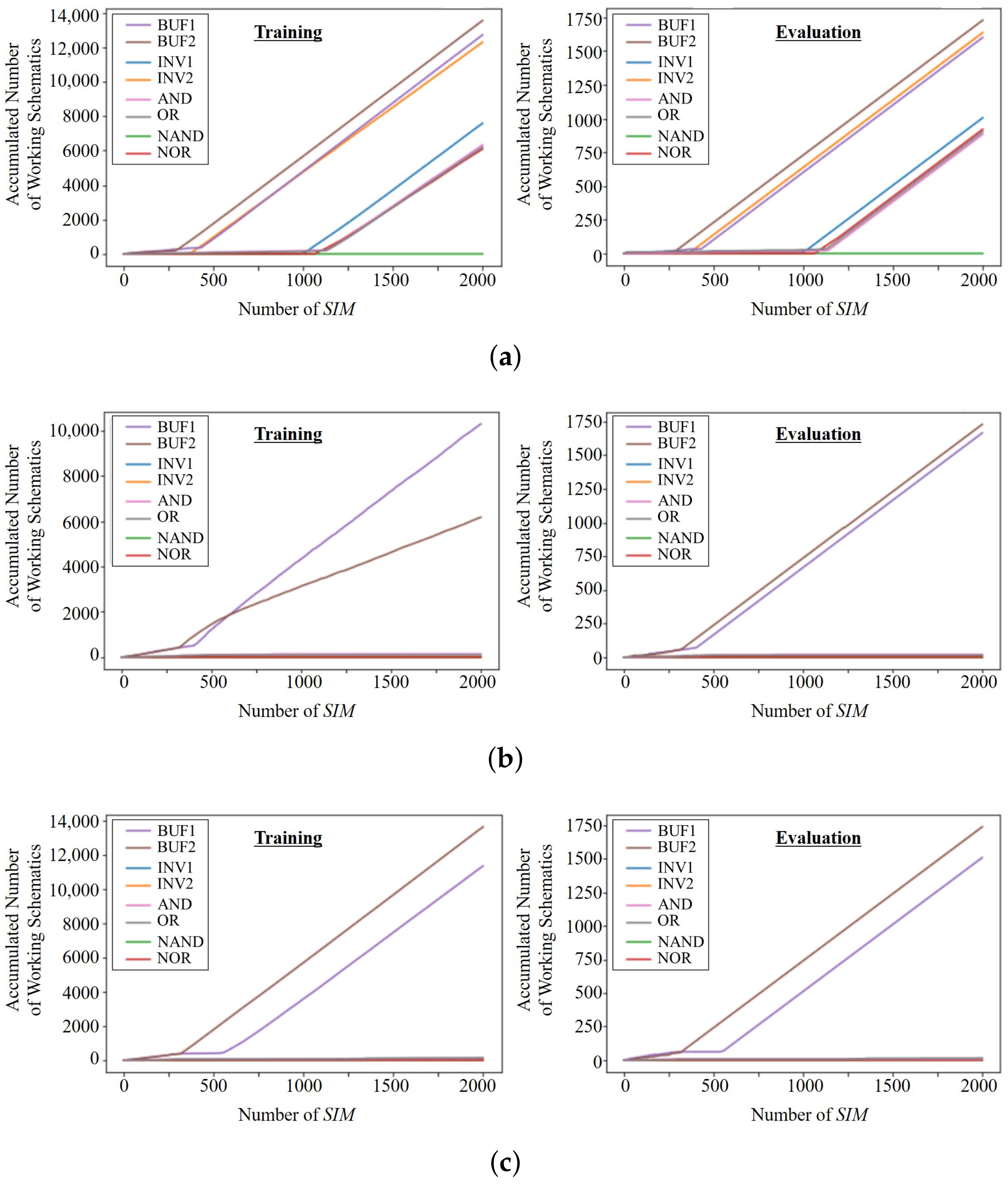
For the agent’s DQN, the numbers of units in , , and are assigned to twice as large as the dimensionality of X () that is 138. The size of is equal to of 126. An -greedy method is adopted with the random action selection probability () of 0.1. The discounting factor, , is 0.95 and the network is optimized by Adam with a learning rate of 0.001. In addition, there exist 8 special replay buffers dedicated to target logic gates (S0RB for BUF1, S1RB for BUF2, S2RB for INV1, S3RB for INV2, S4RB for AND, S5RB for OR, S6RB for NAND, S7RB for NOR) that contain the transition () histories terminated at the reward of +1 and one replay buffers (FRB) for the transitions with the failure where the episode is finished with the reward of −1. All the replay buffers store up to 1024 transitions. On top of multiple replay buffers, the probability of the target logic selection () is adjusted to force the network to focus on the logic gate episodes with more failures, that is, more rewards of −1 at the termination. The network is evaluated at the greedy mode every 64 episodes and the number of extracted working schematics is counted separately for each target logic. Then, those counted values are processed by the Softmax function with the temperature of 0.01 and is obtained by Equation (13). is a vector of 8 elements that includes the counted values for target logic gates.
The numbers of extracted working schematics are plotted in Figure 10a,b for training and evaluation. An x-axis is indicated by the number of s where one is equal to 64 episodes. As expected, BUF1 and BUF2 begin to be extracted first, and then more complicated logics are obtained in the order of AND, OR, INV1, INV2, NAND, and NOR. Especially, because the counted values for BUF1 and BUF2 are much larger than others, their probabilities of the target logic selection are reduced in the training period, which is represented as their smaller slopes in Figure 10a.
The resultant schematics extracted by the proposed GateRL are presented in Figure 11. BUF1 and BUF2 are constructed by one transistor that is always turned on. Their episodes are terminated in 3 steps. AND and OR are proposed with two transistors, where one NMOS transistor is always on, and the other transistor is controlled by . They are finished in 6 steps. When is low and is high for AND, the racing problem between and takes place; however, can be settled at the low level close to GND by increasing the ratio of channel width to channel length of a PMOS transistor (P1). The similar issue on the schematic of OR can be coped with by increasing the channel width-to-length ratio of a NMOS transistor (N2). INV1 and INV2 are composed of one PMOS transistor and one NMOS transistor, and their episodes are done in 6 steps. Lastly, NAND and NOR are built with three transistors (2 PMOS and 1 NMOS for NAND, 1 PMOS and 2 NMOS for NOR), and the episodes end in 9 steps. Like AND and OR, the extracted circuits of NAND and NOR can cause racing problems that would be addressed by manipulating the channel width-to-length ratio. Components and episode lengths of working schematics are summarized in Table 1.
These extracted circuits are evaluated by the off-the-shelf circuit simulator, SPICE, as summarized in Figure 12. The proposed GateRL does not take into account threshold voltages of transistors and racing issues. Therefore, some circuits cannot achieve the rail to rail outputs, even though the channel width-to-length ratio is adjusted. While BUF1 pulls up to the lower voltage than VDD due to the threshold voltage of N1, BUF2 pulls down to the higher voltage than GND due to that of P1. In AND, OR, NAND, and NOR, lower logic-1 than VDD and higher logic-0 than GND are caused by threshold voltage and racing problem. However, all logic-1 and logic-0 voltages are accomplished at higher and lower levels than the center level, respectively. These issues will be further addressed in our future works by revising the verification algorithm for the reward and the network structures.
To verify the necessity of separate replay buffers and adaptive , the GateRL is also trained and evaluated with a uniform or with only one replay buffer. As depicted in Figure 13a, the uniform and separate replay buffers cannot provide NOR schematics within 2000 s, and even other logic gates are extracted at the longer s. In the case of one replay buffer, only BUF1 and BUF2 are designed within 2000 s, as illustrated in Figure 13b,c. Consequently, it is ensured that separate replay buffers can help to find solutions of complicated logic schematics, and the adaptive contributes to improve the training speed.
4. Conclusions
Although various ML algorithms have been employed in many applications, the area of an automated circuit design has not been addressed yet. This paper demonstrates the first ML approach that automatically designs the circuit schematics.
The proposed GateRL is an automated digital circuit design framework based on RL at the backplane of CMOS transistors. The connection of circuit elements is described by CM that is transferred in the format of a vector to the agent along with the mask. The mask is used to reduce the dimensionality of the action space. The agent decides the optimum action of a new connection by a DQN that consists of 4 fully connected network layers. The proposed GateRL is successfully trained with separate replay buffers and adaptive selection probability for 6 target logics, such as buffer, inverter, AND, OR, NAND, and NOR. The extracted schematics are verified by SPICE simulation.
However, the proposed scheme has some limitations. First, all transistors are taken into account as ideal switches by neglecting the threshold voltages. Therefore, the turned-on transistors are dealt with as perfect short circuits regardless of voltage levels at source and drain terminals. Second, some extracted circuits contain the racing problems. These are compensated for to some extent in the SPICE simulation by manipulating the channel width-to-length ratio. Third, only voltage sources and CMOS transistors are included as circuit elements. Even though these limitations, the proposed GateRL will pave the way to the complete ML frameworks of the schematic design over more complicated digital circuits, as well as analog circuits.
Author Contributions
Conceptualization, H.N. and Y.-I.K.; methodology, H.N. and Y.-I.K.; software, H.N.; validation, J.B. and J.L.; formal analysis, H.N.; investigation, H.N.; resources, H.N.; data curation, H.N.; writing—original draft preparation, H.N.; writing—review and editing, H.N.; visualization, J.B., J.L. and H.N.; supervision, H.N.; project administration, H.N.; funding acquisition, H.N. All authors have read and agreed to the published version of the manuscript.
Funding
This research was supported by IDEC (EDA Tool) and the National Research Foundation of Korea (NRF) funded by the Ministry of Science, ICT & Future Planning (NRF-2019R1F1A1061114).
Conflicts of Interest
The authors declare no conflict of interest.
References
- Rawat, W.; Wang, Z. Deep Convolutional Neural Networks for Image Classification: A Comprehensive Review. Neural Comput. 2017, 29, 2352–2449. [Google Scholar] [CrossRef] [PubMed]
- Zhao, Z.Q.; Zheng, P.; Xu, S.T.; Wu, X. Object Detection with Deep Learning: A Review. IEEE Trans. Neural Netw. Learn. Syst. 2019, 30, 3212–3232. [Google Scholar] [CrossRef] [PubMed] [Green Version]
- Saritha, R.R.; Paul, V.; Kumar, P.G. Content based image retrieval using deep learning process. Clust. Comput. 2019, 22, 4187–4200. [Google Scholar] [CrossRef]
- Wang, Z.; Chen, J.; Hoi, S.C.H. Deep Learning for Image Super-resolution: A Survey. IEEE Trans. Pattern Anal. Mach. Intell. 2019. in Press. [Google Scholar] [CrossRef] [PubMed] [Green Version]
- Otter, D.W.; Medina, J.R.; Kalita, J.K. A Survey of the Usages of Deep Learning for Natural Language Processing. IEEE Trans. Neural Netw. Learn. Syst. 2020, in press. [Google Scholar] [CrossRef] [PubMed] [Green Version]
- Nassif, A.B.; Shahin, I.; Attili, I.; Azzeh, M.; Shaalan, K. Speech Recognition Using Deep Neural Networks: A Systematic Review. IEEE Access 2019, 7, 19143–19165. [Google Scholar] [CrossRef]
- Hoseinzade, E.; Haratizadeh, S. CNNpred: CNN-based stock market prediction using a diverse set of variables. Expert Syst. Appl. 2019, 129, 273–285. [Google Scholar] [CrossRef]
- LeCun, Y. Deep Learning Hardware: Past, Present, and Future. In Proceedings of the 2019 IEEE International Solid-State Circuits Conference-(ISSCC), San Francisco, CA, USA, 17–21 February 2019; pp. 12–19. [Google Scholar]
- Dean, J. The Deep Learning Revolution and Its Implications for Computer Achitecture and Chip Design. In Proceedings of the 2020 IEEE International Solid-State Circuits Conference-(ISSCC), San Francisco, CA, USA, 16–20 February 2020; pp. 8–14. [Google Scholar]
- Zhang, C.; Li, P.; Sun, G.; Guan, Y.; Xiao, B.; Cong, J. Optimizing FPGA-based Accelerator Design for Deep Convolutional Neural Networks. In Proceedings of the 2015 ACM/SIGDA International Symposium on Field-Programmable Gate Arrays, Monterey, CA, USA, 22–24 February 2015; pp. 161–170. [Google Scholar]
- Han, S.; Liu, X.; Mao, H.; Pu, J.; Pedram, A.; Horowitz, M.A.; Dally, W.J. EIE: Efficient Inference Engine on Compressed Deep Neural Network. ACM SIGARCH Comput. Archit. News 2016, 44, 243–254. [Google Scholar] [CrossRef]
- Chang, J.W.; Kang, K.W.; Kang, S.J. An Energy-Efficient FPGA-Based Deconvolutional Neural Networks Accelerator for Single Image Super-Resolution. IEEE Trans. Circuits Syst. Video Technol. 2020, 30, 281–295. [Google Scholar] [CrossRef] [Green Version]
- Jouppi, N.P.; Young, C.; Patil, N.; Patterson, D.; Agrawal, G.; Bajwa, R.; Bates, S.; Bhatia, S.; Boden, N.; Borchers, A.; et al. In-Datacenter Performance Analysis of a Tensor Processing Unit. In Proceedings of the 44th Annual International Symposium on Computer Architecture, Toronto, ON, Canada, 24–28 June 2017; pp. 1–12. [Google Scholar]
- Shin, D.; Lee, J.; Lee, J.; Yoo, H.J. DNPU: An 8.1TOPS/W reconfigurable CNN-RNN processor for general-purpose deep neural networks. In Proceedings of the 2017 IEEE International Solid-State Circuits Conference (ISSCC), San Francisco, CA, USA, 5–9 February 2017; pp. 240–241. [Google Scholar]
- Wang, H.; Yang, J.; Lee, H.S.; Han, S. Learning to Design Circuits. arXiv 2018, arXiv:1812.02734. [Google Scholar]
- Settaluri, K.; Haj-Ali, A.; Huang, Q.; Hakhamaneshi, K.; Nikolic, B. AutoCkt: Deep Reinforcement Learning of Analog Circuit Designs. In Proceedings of the 2020 Design, Automation & Test in Europe Conference & Exhibition, Grenoble, France, 9–13 March 2020; pp. 490–495. [Google Scholar]
- Pui, C.W.; Chen, G.; Ma, Y.; Young, E.F.Y.; Yu, B. Clock-aware ultrascale FPGA placement with machine learning routability prediction. In Proceedings of the 2017 IEEE/ACM International Conference on Computer-Aided Design, Irvine, CA, USA, 13–16 November 2017. [Google Scholar]
- Li, Y.; Lin, Y.; Madhusudan, M.; Sharma, A.; Xu, W.; Sachin Sapatnekar, R.H.; Hu, J. Exploring a Machine Learning Approach to Performance Driven Analog IC Placement. In Proceedings of the 2020 IEEE Computer Society Annual Symposium on VLSI, Limassol, Cyprus, 6–8 July 2020. [Google Scholar]
- Crossley, J.; Puggelli, A.; Le, H.P.; Yang, B.; Nancollas, R.; Jung, K.; Kong, L.; Narevsky, N.; Lu, Y.; Sutardja, N.; et al. BAG: A designer-oriented integrated framework for the development of AMS circuit generators. In Proceedings of the IEEE/ACM International Conference on Computer-Aided Design (ICCAD), Santa Clara, CA, USA, 18–21 November 2013; pp. 74–81. [Google Scholar]
- Chang, E.; Han, J.; Bae, W.; Wang, Z.; Narevsky, N.; Nikolic, B.; Alon, E. BAG2: A process-portable framework for generator-based AMS circuit design. In Proceedings of the IEEE Custom Integrated Circuits Conference (CICC), San Diego, CA, USA, 8–11 April 2018. [Google Scholar]
- Hakhamaneshi, K.; Werblun, N.; Abbeel, P.; Stojanović, V. BagNet: Berkeley Analog Generator with Layout Optimizer Boosted with Deep Neural Networks. In Proceedings of the IEEE/ACM International Conference on Computer-Aided Design (ICCAD), Westminster, CO, USA, 4–7 November 2019. [Google Scholar]
- Song, E.; Nam, H. Shoot-through current reduction scheme for low power LTPS TFT programmable shift register. J. Soc. Inf. Disp. 2014, 22, 18–22. [Google Scholar] [CrossRef]
- Song, E.; Nam, H. Low Power Programmable Shift Register with Depletion Mode Oxide TFTs for High Resolution and High Frame Rate AMFPDs. J. Disp. Technol. 2014, 10, 834–838. [Google Scholar] [CrossRef]
- Song, E.; Song, S.J.; Nam, H. Pulse-width-independent low power programmable low temperature poly-Si thin-film transistor shift register. Solid State Electron. 2015, 107, 35–39. [Google Scholar] [CrossRef]
- Kim, Y.I.; Nam, H. Clocked control scheme of separating TFTs for a node-sharing LTPS TFT shift register with large number of outputs. J. Soc. Inf. Disp. 2020, 28, 825–830. [Google Scholar] [CrossRef]
- Sutton, R.S.; Barto, A.G. Reinforcement Learning: An Introduction, 2nd ed.; MIT Press: Cambridge, MA, USA, 2018. [Google Scholar]
- Huang, S.; Ontanon, S. A Closer Look at Invalid Action Masking in Policy Gradient Algorithms. arXiv 2020, arXiv:2006.14171. [Google Scholar]
- Zhang, S.; Tong, H.; Xu, J.; Maciejewski, R. Graph convolutional networks: A comprehensive review. Comput. Soc. Netw. 2019, 6, 1–23. [Google Scholar] [CrossRef] [Green Version]
- Mnih, V.; Kavukcuoglu, K.; Silver, D.; Rusu, A.A.; Veness, J.; Bellemare, M.G.; Graves, A.; Riedmiller, M.; Fidjeland, A.K.; Ostrovski, G.; et al. Human-level control through deep reinforcement learning. Nature 2015, 518, 529–533. [Google Scholar] [CrossRef] [PubMed]
Figure 1.
Proposed GateRL block diagram.
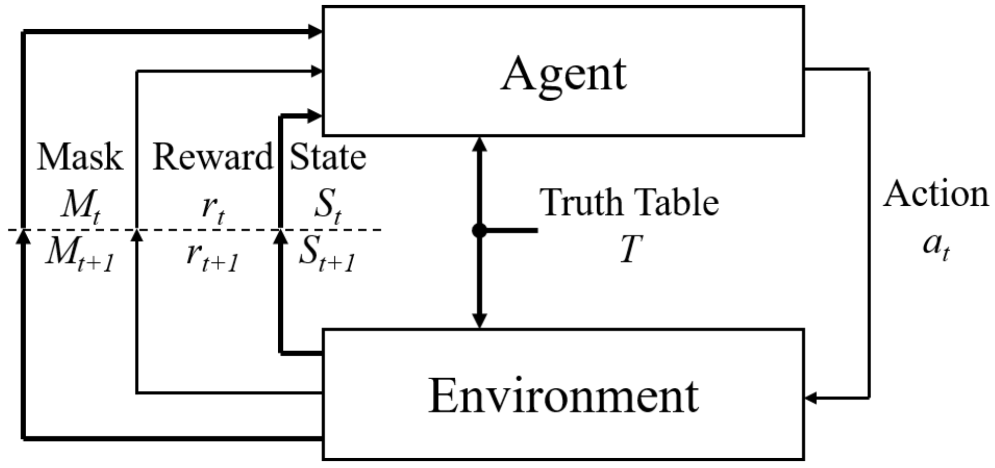
Figure 2.
Connection matrix (CM) configuration.
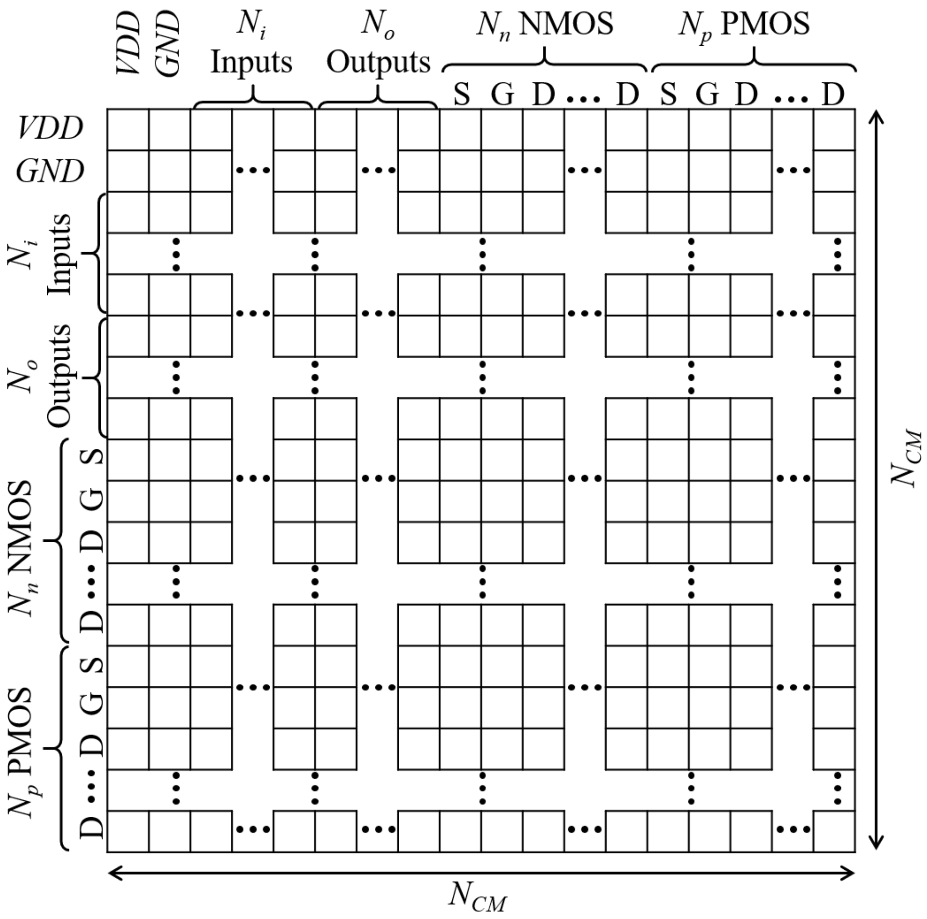
Figure 3.
Example of schematic extraction from a given CM. (a) Example CM. (b) Extracted schematic.

Figure 4.
State definition. Because a symmetric CM does not allow self-connection, as well as connections between VDD, GND, inputs, and outputs, the marked area contains the whole information for CM. They are flattened into a state vector ().
Figure 4.
State definition. Because a symmetric CM does not allow self-connection, as well as connections between VDD, GND, inputs, and outputs, the marked area contains the whole information for CM. They are flattened into a state vector ().

Figure 5.
Mask generation scheme. Based on a given CM, MM is generated according to four masking criteria. The red 1s of matrices in the middle are existing connections in CM, and the blue 1s are possible connections via other nodes for each masking criterion. Finally, two vectors of and are produced by flattening the upper right regions of CM and MM, respectively.
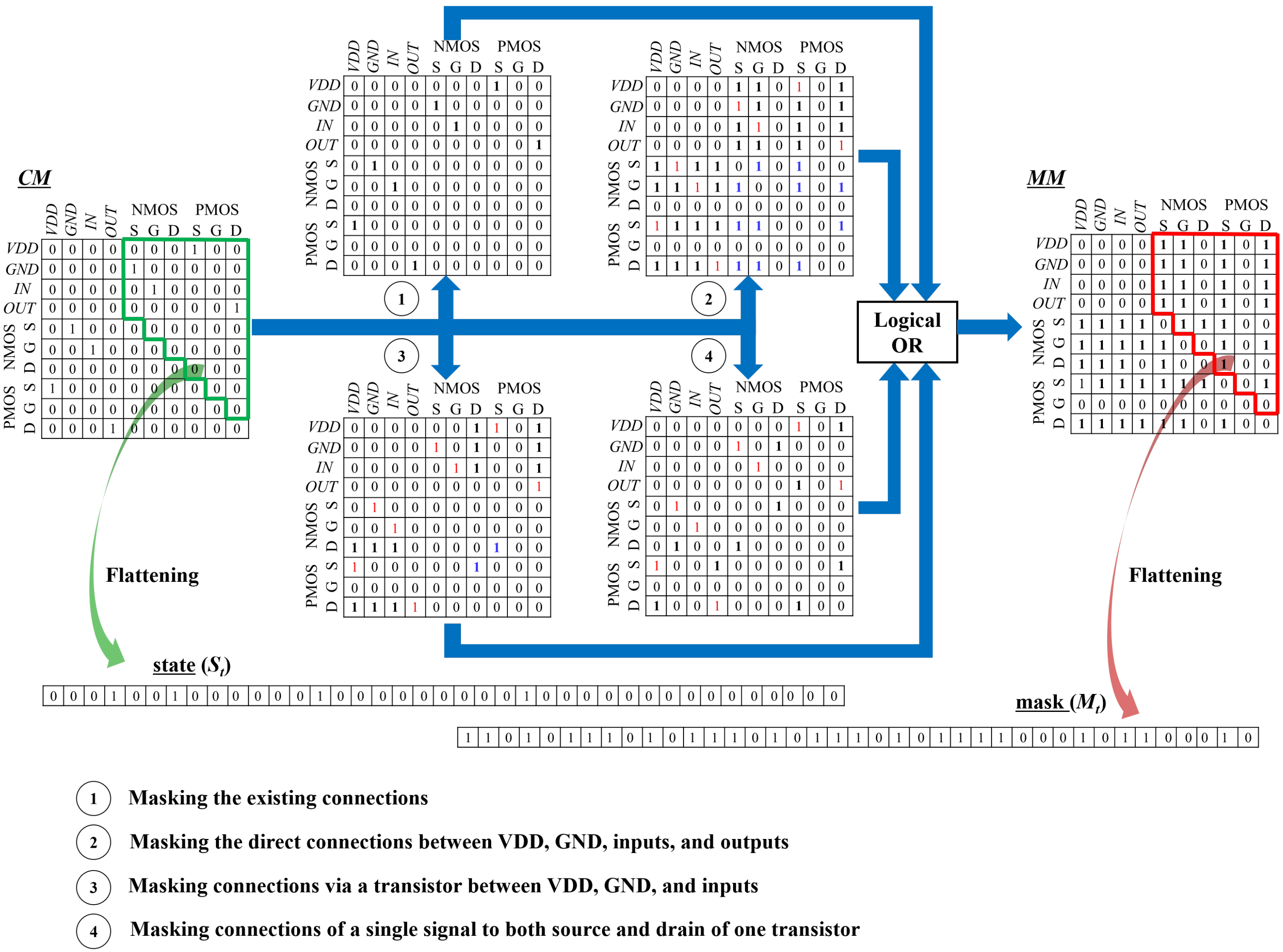
Figure 6.
Truth table for an inverter circuit. Because it is an one-input gate, is kept at high impedance by assigning 0, where +1 is VDD, and −1 is GND.
Figure 6.
Truth table for an inverter circuit. Because it is an one-input gate, is kept at high impedance by assigning 0, where +1 is VDD, and −1 is GND.
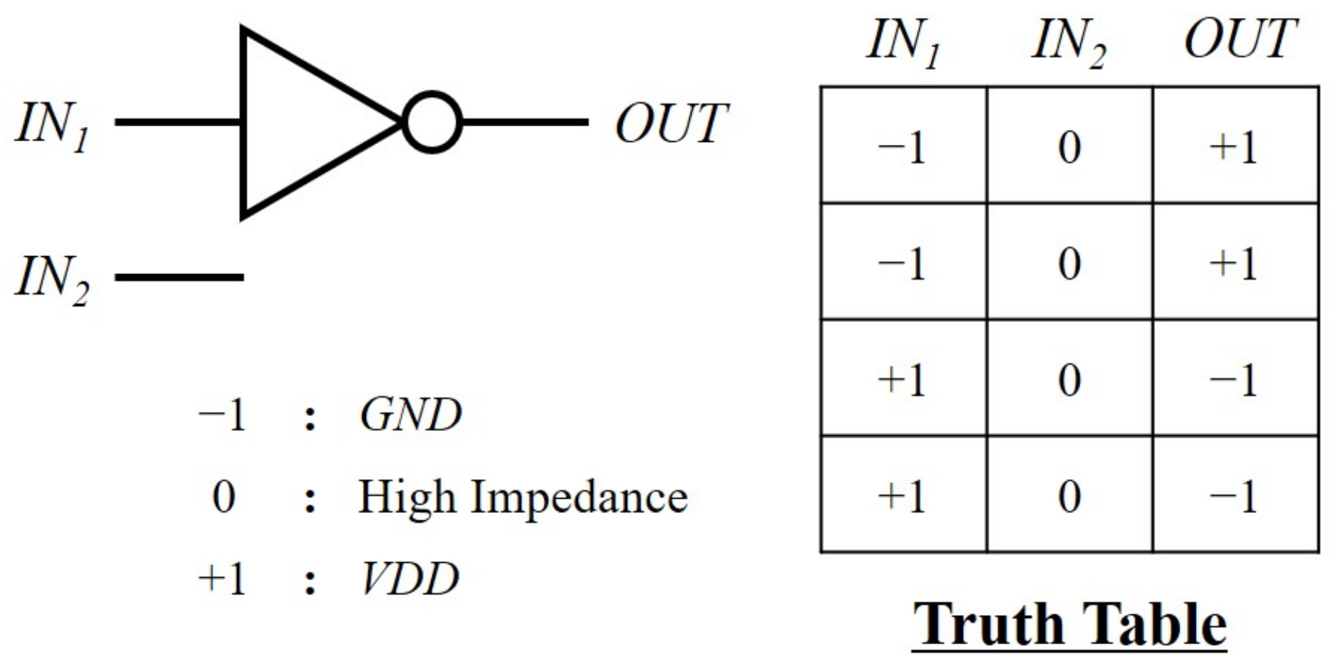
Figure 7.
Verification steps for an inverter. Since outputs for all inputs () are matched to target outputs (), is decided as +1.
Figure 7.
Verification steps for an inverter. Since outputs for all inputs () are matched to target outputs (), is decided as +1.
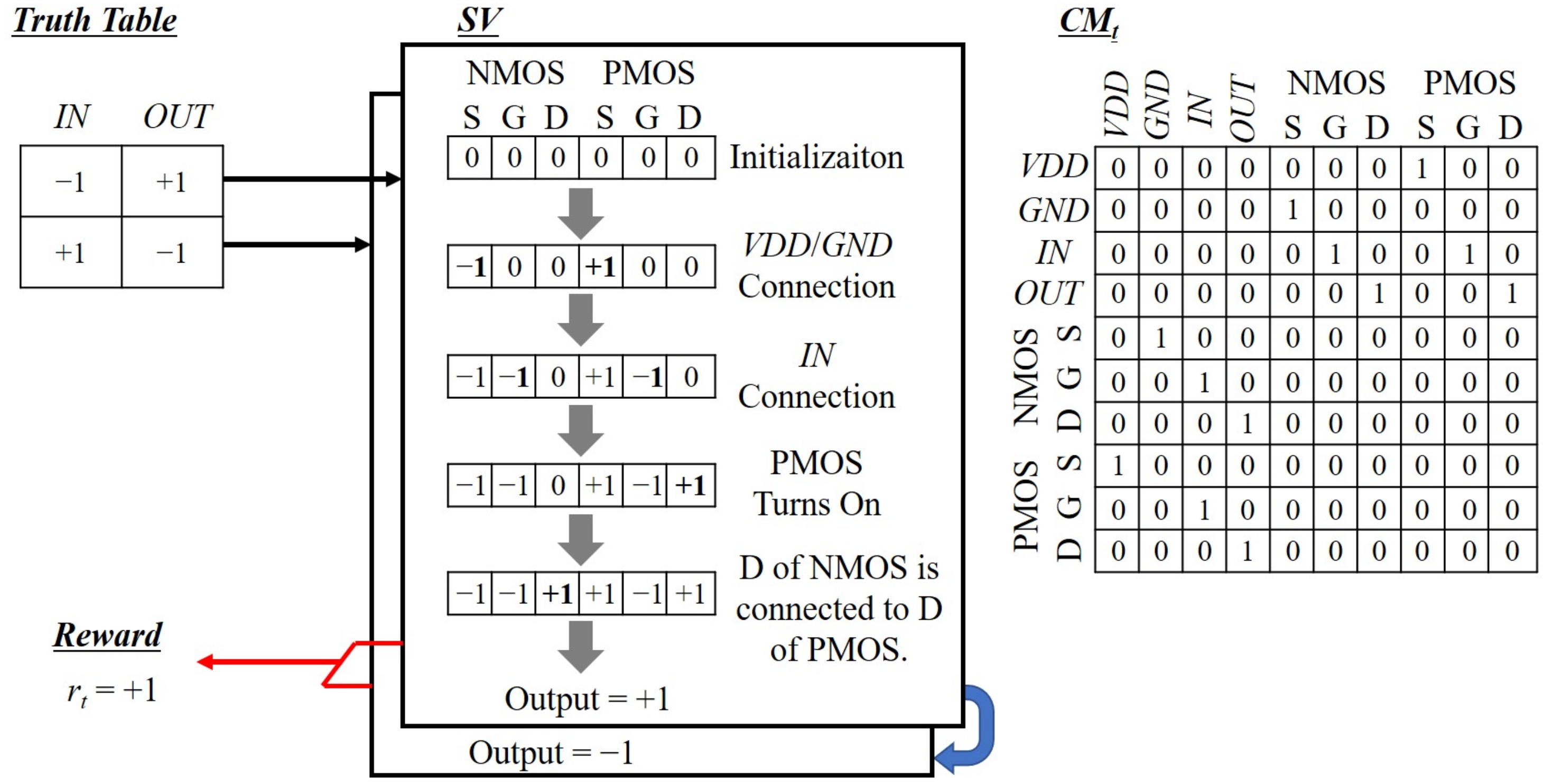
Figure 8.
DQN structure. It deals with the concatenation of and T as an input layer. The range of elements from 0 to 1 is extended from −1 to +1 in order to be matched to T.
Figure 8.
DQN structure. It deals with the concatenation of and T as an input layer. The range of elements from 0 to 1 is extended from −1 to +1 in order to be matched to T.
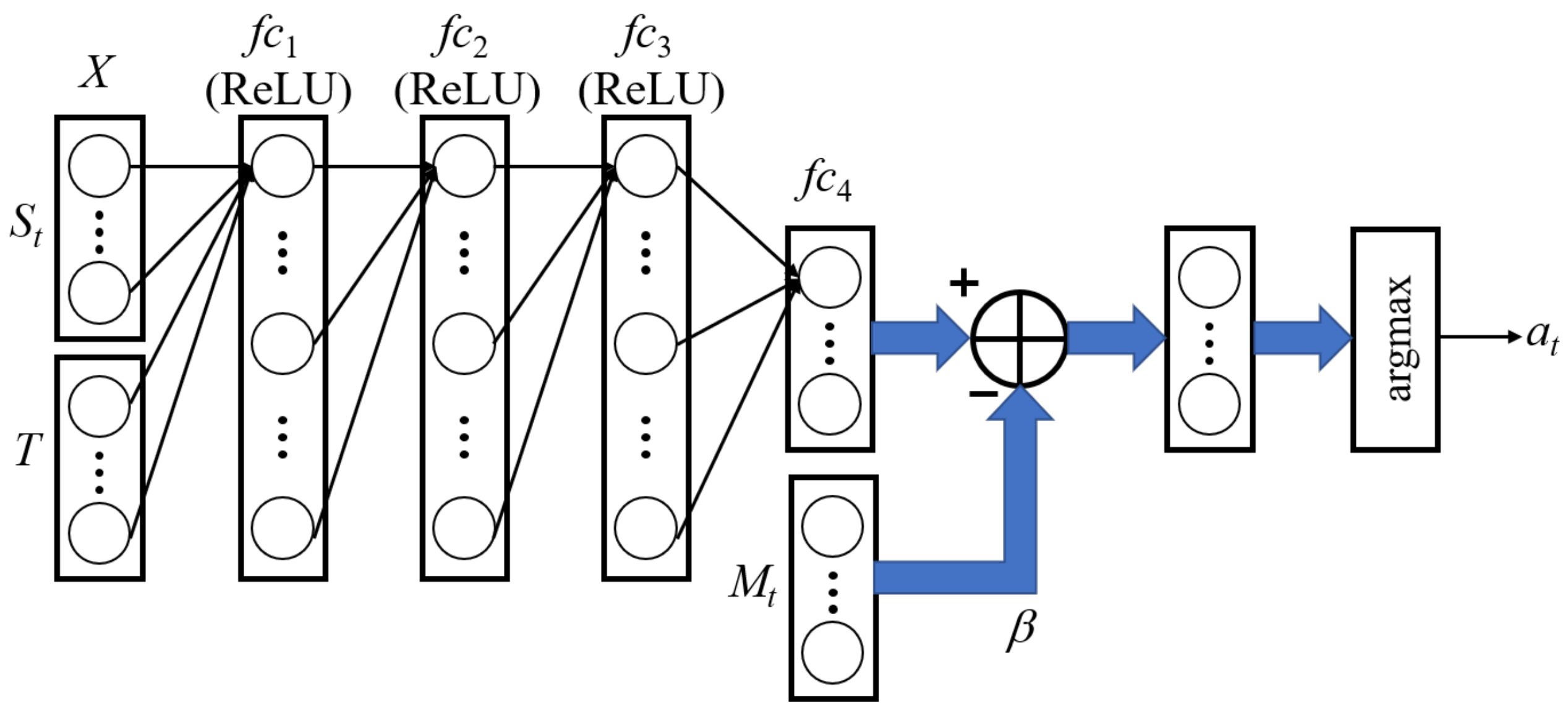
Figure 9.
Truth tables for target logic gates. While BUF1 and INV1 are buffer and inverter with an input of , BUF2 and INV2 are buffer and inverter with an input of .
Figure 9.
Truth tables for target logic gates. While BUF1 and INV1 are buffer and inverter with an input of , BUF2 and INV2 are buffer and inverter with an input of .
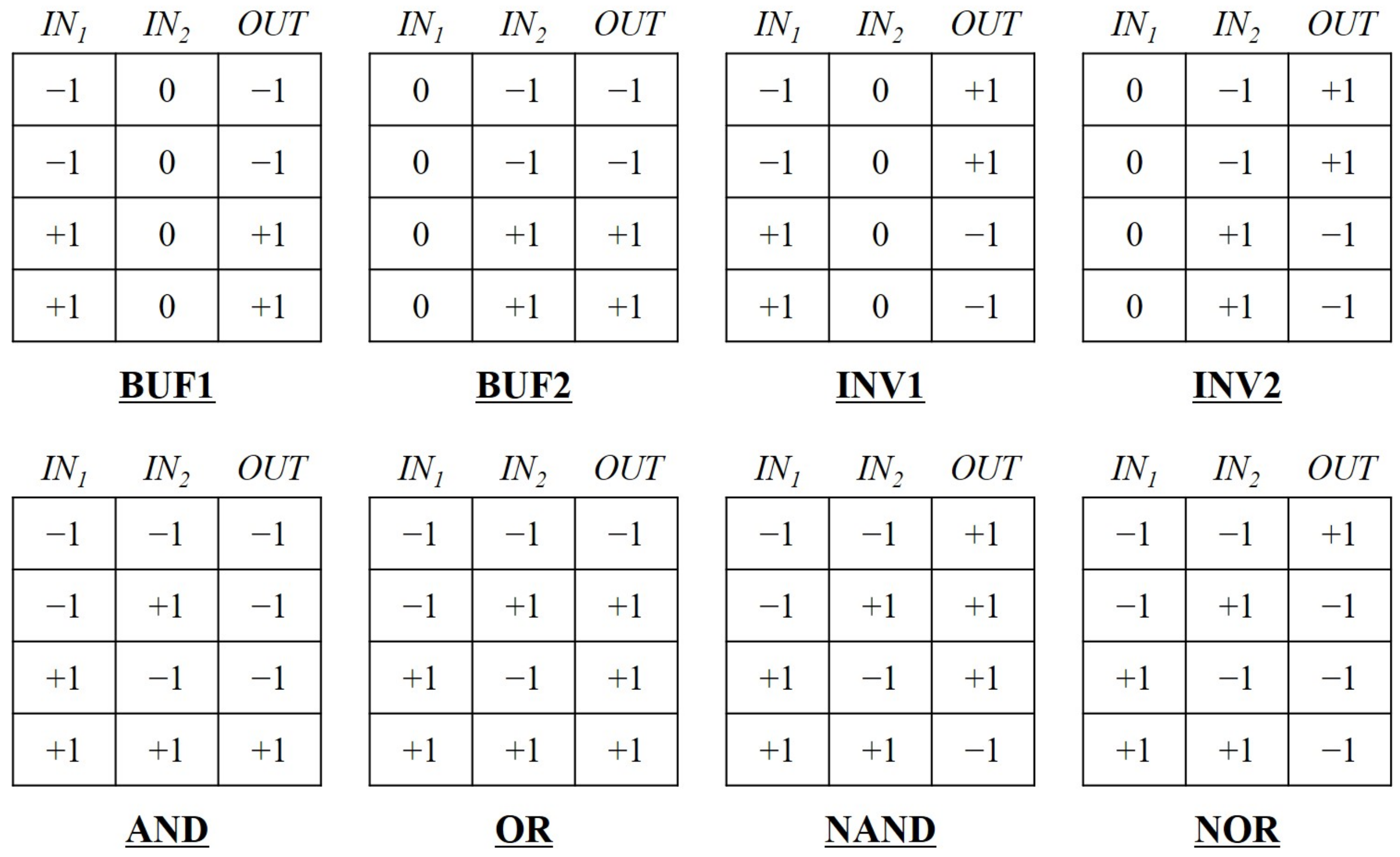
Figure 10.
Plots of the number of extracted working schematics for target logic gates. (a) Training. (b) Evaluation.
Figure 10.
Plots of the number of extracted working schematics for target logic gates. (a) Training. (b) Evaluation.
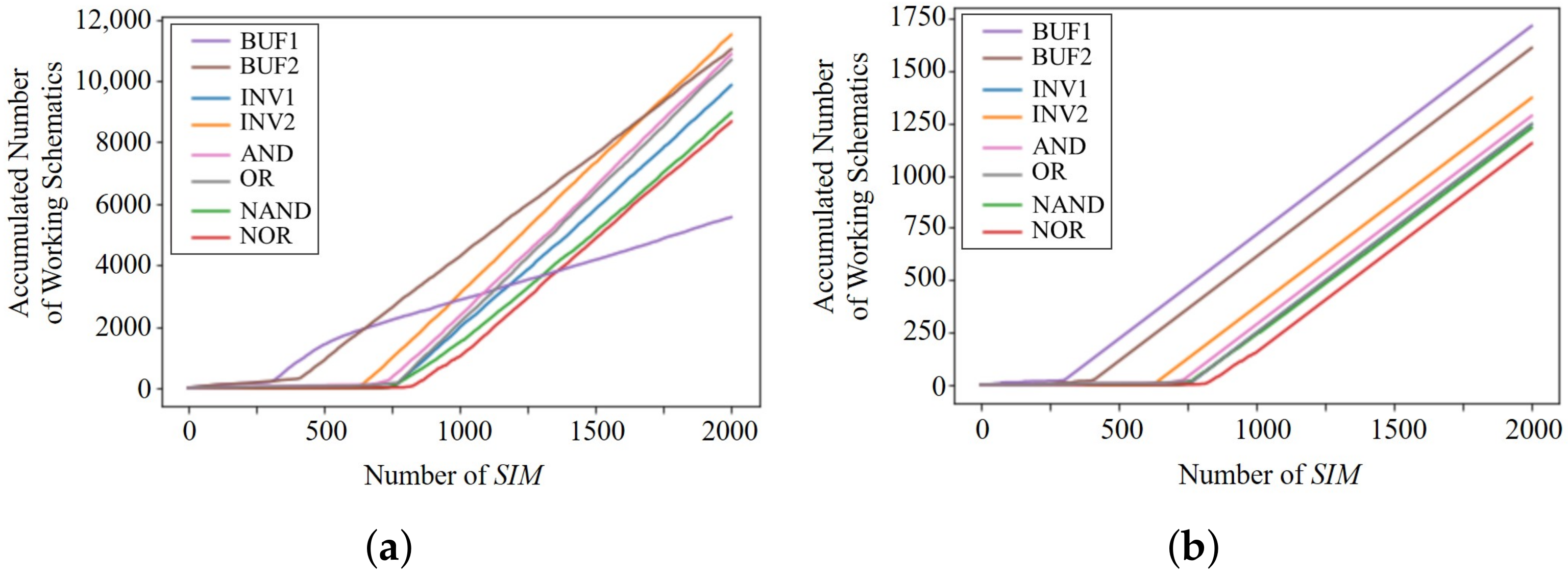
Figure 11.
Working schematics extracted by GateRL for target logic gates.

Figure 12.
SPICE simulation results.
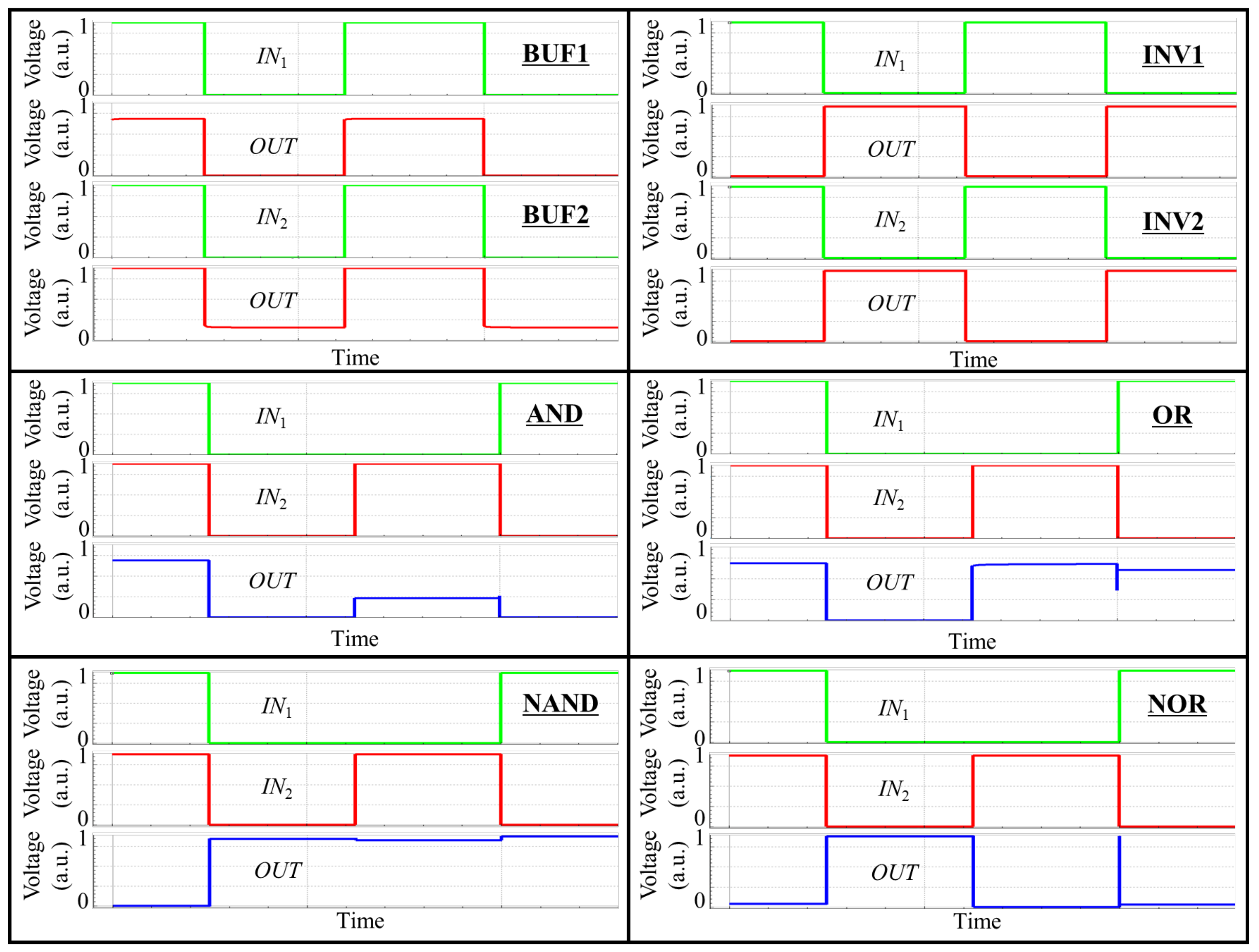
Figure 13.
Plots of the number of extracted working schematics for target logic gates. (a) With a uniform and separate replay buffers (b) With an adaptive and one replay buffer. (c) With a uniform and one replay buffer.
Figure 13.
Plots of the number of extracted working schematics for target logic gates. (a) With a uniform and separate replay buffers (b) With an adaptive and one replay buffer. (c) With a uniform and one replay buffer.

Table 1.
Training results for target logic gates.
| Target Logic Gate | Components | Episode Length |
|---|---|---|
| BUF1 | 1 NMOS | 3 Steps |
| BUF2 | 1 PMOS | 3 Steps |
| INV1 | 1 NMOS, 1 PMOS | 6 Steps |
| INV2 | 1 NMOS, 1 PMOS | 6 Steps |
| AND | 1 NMOS, 1 PMOS | 6 Steps |
| OR | 2 NMOS | 6 Steps |
| NAND | 1 NMOS, 2 PMOS | 9 Steps |
| NOR | 2 NMOS, 1 PMOS | 9 Steps |
Publisher’s Note: MDPI stays neutral with regard to jurisdictional claims in published maps and institutional affiliations. |
© 2021 by the authors. Licensee MDPI, Basel, Switzerland. This article is an open access article distributed under the terms and conditions of the Creative Commons Attribution (CC BY) license (https://creativecommons.org/licenses/by/4.0/).
Share and Cite
MDPI and ACS Style
Nam, H.; Kim, Y.-I.; Bae, J.; Lee, J. GateRL: Automated Circuit Design Framework of CMOS Logic Gates Using Reinforcement Learning. Electronics 2021, 10, 1032. https://doi.org/10.3390/electronics10091032
AMA Style
Nam H, Kim Y-I, Bae J, Lee J. GateRL: Automated Circuit Design Framework of CMOS Logic Gates Using Reinforcement Learning. Electronics. 2021; 10(9):1032. https://doi.org/10.3390/electronics10091032
Chicago/Turabian StyleNam, Hyoungsik, Young-In Kim, Jina Bae, and Junhee Lee. 2021. "GateRL: Automated Circuit Design Framework of CMOS Logic Gates Using Reinforcement Learning" Electronics 10, no. 9: 1032. https://doi.org/10.3390/electronics10091032
Note that from the first issue of 2016, this journal uses article numbers instead of page numbers. See further details here.