
Linearization as a Solution for Power Amplifier Imperfections: A Review of Methods


1
Department of Computer Science and Communications Technologies, Vilnius Gediminas Technical University, 03227 Vilnius, Lithuania
2
Micro and Nanoelectronics Systems Design and Research Laboratory, Vilnius Gediminas Technical University, 10223 Vilnius, Lithuania
*
Author to whom correspondence should be addressed.
Electronics 2021, 10(9), 1073; https://doi.org/10.3390/electronics10091073
Submission received: 8 April 2021
/
Revised: 27 April 2021
/
Accepted: 29 April 2021
/
Published: 1 May 2021
(This article belongs to the Section Power Electronics)
Abstract
:Development of 5G networks requires a substantial increase to both spectral and power efficiency of transmitters. It is known that these two parameters are subjected to a mutual trade-off. To increase the linearity without losing power efficiency, linearization techniques are applied to power amplifiers. This paper aims to compare most popular linearization techniques to date and evaluate their applicability to upcoming 5G networks. The history of each respective linearization technique is followed by the main principle of operation, revealing advantages and disadvantages supported by concluding the latest research results. Three main groups of linearization methods currently known are feedforward, feedback, and predistortion, each with its own tradeoffs. Although digital predistortion seems to be the go-to method currently, other techniques with less research attention are still non-obsolete. A generalized discussion and a direct comparison of techniques analyzed are presented at the end of this paper. The article offers a systematic view on PA linearization problems which should be useful to researchers of this field. It is concluded that there are still a lot of problems that need to be addressed in every linearization technique in order to achieve 5G specifications.
1. Introduction
Despite the already high performance and reliability of 4G technology wireless systems, the telecommunications industry and academia are looking for new ways to further improve data rates, connection densities, and latencies by developing next generation 5G wireless standards and future network models. Compared to 4G communication networks, 5G wireless communication technologies are planned to achieve user experienced data rates from 100 Mbps to 1 Gbps, reliable connection densities of up to 1 million per square kilometer, end-to-end latency in the millisecond level, frequency bandwidths of up to 150 MHz, and mobility of up to 500 km/h [1]. The target parameters are planned to be obtained using sub-6 GHz/cm-Wave/mm-Wave spectrum frequency carriers, together with spectrally efficient modulation waveforms, and large numbers of beamforming antennas for massive MIMO and rapidly evolving GaN, GaAs, SiGe, and Si-LDMOS technologies [2]. As a result, 5G wireless networks will connect a wide range of devices that support a variety of communication standards and bands. This is expected to utilize a massive amount of MIMO multichannel and multi-standard RF transceivers with a highly integrated density of RF power amplifiers (PA’s), making the PA’s PAE, cost, and small form-factors particularly critical to the mission success of the 5G revolution [3].
The efficiency of RF PA directly affects the efficiency of any transmitter, so emerging 5G wireless technologies require new PA architectures that improve efficiency without losing linearity. It is widely known that the RF PA is the most power-consuming component in RF transceivers and, at the same time, occupies an important place in the data transmission circuit. Researchers must find a compromise between key RF PA parameters such as linearity, output power, and PAE. With the classical RF PA architecture, it is not possible to optimize all key parameters without significantly degrading at least one. A universally accepted solution to this problem today is the design of a power efficient amplifier, which is later linearized. This paper is dedicated towards outlining and explaining the most widely used linearization methods, as well as reviewing the last results obtained.
Linearization is currently the main way to resolve the conflict between growing energy and spectrum efficiency requirements. The contradiction arises from the use of increasingly higher order signal modulations for higher spectral efficiency. This inevitably increases the ratio between the mean and peak signal values, i.e., peak-to-average power ratio (PAPR). An increase in this ratio requires an increase in the amplifier’s linear range. Without the use of any linearization techniques, the amplifier must be used in class A mode with a considerable power back-off, which in turn, significantly reduces the energy efficiency of the system. This problem has been known and solved for a long time, but in order to achieve the goals set by 5G, it is becoming more and more relevant again.
Our paper consists of four sections: introduction, overview, discussion, and conclusions. The introduction section is followed by the overview section, in which general linearization techniques, their operation principles, and concrete implementations are reviewed. The discussion section consists of the summary of methods reviewed and authors’ observations on the matter. The paper is concluded with summary and suggestions for further research directions. We attempt to systematically show the development of the problem and solutions presented in the literature thus far. We offer analyses and comparison of the research in this field. This work serves as an in-depth introduction to a wide, deep, and interesting power amplifier linearization problem.
2. Overview
The linearization problem can be visualized by inspecting the general transfer characteristic of a power amplifier (Figure 1). Ideally, we would like to have a transfer characteristic that is linear up until the clipping point, but, due to physics of semiconductors, this is not the case in transistor amplifiers. It can be seen that the transfer characteristic splits into three parts: linear region, nonlinear region, and saturation region. It is known that an amplifier is most energetically efficient in the saturation region of the stransfer characteristic. In case when the constant amplitude signal is amplified, it is possible to set a quiescent point (Q point in Figure 1) near the amplifier’s saturation point (S point in Figure 1). However, when we are aiming for spectral efficiency, we are, generally, forced to use variable amplitude signals. In order to transfer signals with variable amplitude, we need to move Q point down to the amplifier’s linear range, this, in turn, reduces the amplifier’s power efficiency. When the Q point is set in a way that allows it to amplify whole signal amplitude linearly, the amplifier is considered to be class A. This is a basic linearization technique that uses power back-off (which is a difference between S point power and Q point power, either in input power terms or output power terms) and is highly spectrally efficient but also extremely energetically inefficient. Maximal theoretical efficiency of class A amplifier is 50% but, due to practical limitations, may fall below 25%. By extending the amplifier’s linear range, we can move Q point closer to S point, reduce the required power back-off (ideally power back-off should not exceed input signal’s amplitude), and improve power efficiency.
The best way to achieve both spectrally and energetically efficient amplification today is to linearize the nonlinear transfer characteristic of an energetically efficient amplifier. There are three common linearization techniques that will be reviewed in following sections: feedforward, feedback, and predistortion. Every section is concluded by the table listing of respective method results.
2.1. Feedforward Linearization
The feedforward linearization technique was the first invented linearization method but was widely adopted later than other linearization methods [4]. This can be explained by reviewing the principle of the feedforward operation and the development of communication technologies. The operational diagram of the method is given in Figure 2. The feedforward circuitry attempts to isolate an error generated by a main amplifier so that this error can be further minimized, or ideally, completely eliminated from the output signal. The feedforward circuitry consists of signal and error cancelation sub-circuits. The signal cancelation circuit isolates the error of the main amplifier, and the error cancelation circuit subtracts the received error from the main signal.
The input signal is divided into two parts, one of which is fed to the input of the power amplifier; the other is delayed by Td3 and fed to the comparator of the signal cancellation circuit. For simplicity, we assume that coupling ratio B >> 1 so that the coupler has no noticeable effect on the input and output signal powers of the amplifier. The output signal of the main amplifier consists of the sum of the amplified input signal and the interference generated by the amplifier (AVin + Vd). Part of the output signal is coupled to the signal cancelation loop comparator via an attenuator. By setting the delay time Td3 so that it compensates for the delays caused by the main amplifier and the attenuator, i.e., Td3 = Td1 + Td2, at the output of the signal cancellation comparator, one will ideally obtain the attenuated value of the distortions generated by the main amplifier. The value obtained in the signal cancellation circuit is then amplified by an error amplifier and fed to an output comparator. The delay time Td5 = Td2 + Td4 ensures the same phases of both compared signals. Ideally, the error signal is subtracted from the main amplifier signal, receiving a distortion free signal at the output.
The concept of the feedforward method is intuitive and simple, but it was clear to Howard Black, the developer of the methodology, that the implementation of this concept has many practical difficulties with respect to the stability of component parameters [4,5]. The accuracy of the circuit parameters has a decisive influence on the value of nonlinear distortion suppression, since almost identical values are compared. During his time, Howard Black faced the problem that the vacuum tube amplifiers used did not have sufficient stability in temperature, age, and frequency parameters. For example, the feedforward amplifier system he developed had to be manually adjusted every six hours because the fluctuation in supply voltage caused gain change, which drastically lowered distortion suppression. Eventually, Black solved his problem by developing another linearization technique—feedback linearization, which we will discuss later. The feedforward method was more or less forgotten up until the early 1970s.
By the 1970s, vacuum tube amplifiers were starting to be replaced by solid-state devices. Communication networks were expanding, and solutions were needed to ensure the use of wider bandwidth channels. Around this time, researchers returned their attention to feedforward amplifiers. In 1973, researchers T. J. Bennett and R. F. Clements published an article [6] reviewing the disadvantages of the feedback linearization technique and the potential advantages of the feedforward method. The authors noted that, as the frequencies of the signals used increased, the gain and phase margins of feedback structure decreased, and, therefore, it became more difficult or even impossible to ensure circuit stability. Several years earlier, similar statements were made by H. Seidel et al. [7]. H. Seidel contended that the feedback method faced the problem of causality. The problem was at the heart of the feedback method—one attempts to correct an event that has already happened by changing its cause. This works up to a certain limit when the “past” and the “present” are not clearly separated in terms of the signal, i.e., the delay of the amplifier is much shorter than the period of the received signal. As the signal period approaches the amplifier delay time, this limitation arises, and the contradiction of the method becomes apparent—unwanted oscillation occurs at the amplifier output. Unlike feedback, the feedforward circuit structure is unconditionally stable at all frequencies, because the signal is compared to a time delayed reference signal. This advantage of feedforward was a cornerstone that often did not even leave a real choice between the two methods. Together with this main advantage, feedforward also has a less drastic reduction in gain compared to feedback, does not depend on the delay nature of the amplifier used, and does not require the use of a portion of the gain–bandwidth product to ensure amplifier stability.
After identifying all the potential advantages of feedforward, it was necessary to come up with ways to minimize or circumvent the shortcomings of this structure. The disadvantages of feedforward can be roughly divided into two groups: distortions due to extremely high requirements for component tolerance and power losses due to additional amplifier and passive components. The stability of the values of the components used is critical when the circuit compares two nearly identical signals. Unlike feedback, feedforward does not have a self-regulating mechanism to compensate for component value shifts due to temperature, age, supply voltage fluctuations, and so on. This means tha, t as the environmental conditions change, the classical feedforward scheme collapses quickly. Therefore, in order to achieve an acceptable distortion suppression value, it is necessary to provide a way to compensate for natural fluctuations in the values of the elements of the circuit. There are also questions about the power efficiency of such a structure. The error amplifier used must not introduce its own distortions in the signal, which usually means that it must be used in class A mode with a significant power back-off. In addition, the use of additional couplers and comparators inevitably reduces the power efficiency of the system. Researchers have been working on these problems since the 1970s.
Additional power loss is one of the serious factors limiting the use of feedforward. When developing this methodology, Black was primarily thinking about reducing intermodulation distortions, and energy efficiency was a secondary consideration for him. Today, in order to reduce the energy consumption of communication networks, the energy efficiency of the amplifier system requires much attention. From an energy efficiency point of view, an additional power amplifier in the error cancellation circuit becomes a key issue in the feedforward system. The power consumed by the error amplifier is not directly used to amplify the input signal, so its amount is inversely proportional to the total value of the system power efficiency factor. One of the factors that determines the power consumed by the error amplifier is the amplifier’s output power coupler ratio. By transferring more power to the error cancelation circuit, one can use a lower power error amplifier, but this reduces the output power level, because there is no way to compensate for the losses caused by the power coupler. This problem is solved by selecting the optimal coefficients of the utilized power couplers. Reactive devices (such as transformers) can also be used instead of hybrid directional couplers, sacrificing insulation between the main and error correction circuits for lower power losses.
With certain assumptions, [6,8,9] papers provide a quantitative theoretical analysis of feedforward circuit power efficiency parameters. The authors single out the main factors determining power efficiency: variation of the gain of the main amplifier in the signal bandwidth, the value of the output coupler, and total insertion losses of time delay elements. The power consumption of the error amplifier increases as the variation of the gain of the main amplifier increases. For example, if the gain of the main amplifier drops by 2 dB in the bandwidth and the phase fluctuates by ± 9°, the error amplifier must provide −12 dB of power compared to the main amplifier. Similarly, the relative power of the error amplifier can be calculated for other values of gain and phase variation [6]. The theoretical dependence of power efficiency on the value of the output coupler used is given in [8]. This study shows that the peak value of the efficiency curve is sharply defined using more efficient amplifiers (e.g., with a class C power amplifier, the feedforward system achieves a theoretical efficiency of 43.25% at an 8.2 dB output coupler value). In the case of less efficient amplifiers in the system, the peak of the efficiency curve is wider (e.g., with a class A amplifier, the feedforward system achieves a theoretical power efficiency of 24.1% at 17.6 dB output coupler value. However, when increasing coupler value by 10 dB, efficiency drops only by 1.6% to 22.5%). Although both these results are only approximate due to the assumptions made, the dependence revealed is illustrative. Further mathematical analysis showed that the efficiency of the feedforward circuit drops drastically when estimating the insertion losses of the time delay elements [9]. For example, a 1 dB input loss reduces the efficiency of the theoretical Class C amplifier feedforward system from 43% to ~34%, and a 2 dB input loss reduces the theoretical efficiency to ~28%.
To solve the problem of low component tolerance and natural parameter drift, adaptive feedforward linearization technique is used. To our knowledge, one of the first to theoretically investigate this method was J. K. Cavers [10,11]. In his work, he investigated the adaptation parameters of a so-called gradient feedforward amplifier. The essence of the method is to adjust the parameters of the feedforward circuit (delay time, complex gain, etc.) using a mathematically calculated gradient signal.
Analyzing the feedforward circuit, J. K. Cavers found that the accuracy α of the signal cancellation circuit elements must be in the order of 10−4 over the entire signal frequency range to achieve 40 dB IM distortion attenuation.
where β is the unity gain of error amplifier, IMSRa and IMSR0 are the ratios of intermodulation power to signal power before and after the error cancellation circuit, respectively. For example, to suppress intermodulation interference by 40 dB, one needs an accuracy of 1% in error amplifier parameters in the whole bandwidth. It has also been determined that the error in the delay times of the branches of the circuit must not exceed 0.3% of the signal period. For example, to achieve 40 dB intermodulation distortion suppression when a 10 MHz bandwidth signal is used, the maximum delay time error τ is calculated in Equation (2). Considering that 5G aims to use bandwidths considerably higher than 10 MHz, simple feedforward delay elements accuracy requirements can easily become unpractical.
One of the shortcomings of the analysis is that it ignores the memory effects of the amplifier. The least mean squares adaptation estimating the amplifier memory effects using the Wiener–Hammerstein memory model has been thoroughly investigated in [12]. Both analyses propose methods to alleviate the component tolerance requirements for the feedforward circuit. A method of a pilot signal adaptation has also been described in the literature [13]. Unlike the gradient method, this method adds a pilot signal outside of the channel bandwidth to the input signal. The power of the added signal is then measured at the output, thus evaluating the level of distortion suppression and adjusting the parameters of the error cancellation circuit.
Table 1 shows the best results obtained with the feedforward method to the best of the authors’ knowledge. Studies were selected that took the following into account: the date of publication—only the results of the last 15 years were included; whether the work provided a measurement of a physical prototype; and whether both spectral and energy efficiency parameters were specified.
Five works were investigated according to the specified criteria. The highest achieved energy efficiency was 27.2% (drain efficiency) and 19.4% PAE. The highest achieved Adjacent channel leakage ratio was −63 dBc. The best ratio of spectral to energy efficiency was demonstrated in R. N. Braithwaite’s 2013 work [17]. Typically, the error amplifier is set to Class A or AB, which significantly reduces the efficiency of the feedforward circuit. In the mentioned study, the error amplifier was a nonlinear Doherty structure amplifier. By appropriately controlling the nonlinear distortions generated by the main amplifier, the author determined a mode of operation in which the distortions generated by the main amplifier were inverse to the distortions created by the error amplifier; thus, these distortions compensate for each other. This is achieved by including an offset calculated in the value function.
2.2. Feedback Linearization
As mentioned earlier, the feedback linearization technique was developed by the same author as the feedforward technique. While, today, feedback is one of the most often used design techniques for amplifiers, it is interesting to note that, in an initial attempt to patent it, the patent was denied, because this method was thought to be some variation of the perpetual motion machine. However, later, due to its simplicity and efficiency, this methodology became widely used in lower frequency amplifiers. A simplified operational diagram of the feedback circuit is given in Figure 3.
Mathematical interpretation of the operation of a feedback circuit is given below. It is known that, algebraically, the output signal Vout of an amplifier can be described as follows:
where V is the input signal, kn is the weight of the corresponding harmonic. Ideally, all kn with coefficients n > 1 are equal to 0. Of course, virtually any amplifier distorts the shape of the input signal and creates new spectral components. If part of the signal β is returned to the amplifier’s input via the negative feedback circuit, the expression of the output signal can be overwritten [19]:
where
The simplest feedback circuit reduces the amplitudes of the side harmonics by a factor of 1/(1 + k1β). It is not difficult to notice that, together with the side harmonics, distortions caused by other reasons are suppressed: temperature, age, supply voltage fluctuations, etc., so in general, the feedback circuit does not require additional system adjustment. It is also said that feedback is a self-regulating circuit. It can also be shown that, in the case of negative feedback, the frequency-dependent gain is replaced by a much smaller but more stable feedback gain. The physical essence of this process is that, by turning the phase of the output signal by 180° and returning it to the input, the power of the generated side harmonics is subtracted from the input signal so it can be later compensated by the amplifier. This methodology is applied at relatively low frequencies, but the transition to RF and microwave reveals a contradiction in causality that we described earlier. This contradiction is partially resolved by using part of the gain–bandwidth to ensure stability, i.e., creating sufficient gain and phase margin. It is also obvious that returning part of the output signal to the input results in an irreversible loss of the output signal power. It is not difficult to notice that, in the case of simple feedback, the attenuation of side harmonics in decibels is equal to the value of the gain in decibels lost [20]. The problems of ensuring stability and compensating for gain reduction are relatively easily solved in low frequency systems but are much more difficult to solve at higher frequencies. This is because, as the frequencies increase, each decibel of the gain becomes technologically more expensive, and the delay of the feedback circuit approaches the propagation rate of the signal.
In order to use feedback linearization at RF frequencies, a number of different methods have been proposed [20,21,22]: active feedback, envelope feedback, polar feedback, and Cartesian feedback. These are the most widely used feedback methods. At the same time, references to so-called distortion and difference-frequency methods can be found in the literature, but they are rarely used and will not be discussed in more detail.
The active feedback methodology was proposed by Ballesteros et al. [23,24,25] in the mid-1980s. A simplified operational diagram of active feedback is shown in Figure 4. Passive component feedback is replaced by active component feedback. Couplers C1 and C2 are also used in the system, whose values are adjusted to achieve optimal system performance. It is clear from (4) that the greater the portion of the output signal returned to the input, the greater the attenuation of the side harmonics. By using active components in the feedback circuit, it is possible to ensure the suppression of intermodulation distortions of the same magnitude by using a smaller part of the output signal power. It is also possible to suppress the intermodulation distortions of the main amplifier by controlling the operational point of the secondary amplifier. To do so, the form of the distortion in the secondary amplifier must be complementary to the distortion form generated by the main amplifier. The authors were able to demonstrate a 3.2 dB increase in output power at the same level of distortion compared to a conventional feedback scheme [23]. However, at the same time, it was noted that such a system was sensitive to changes in temperature due to the variation in gain of the secondary amplifier. Therefore, one of the main advantages of feedback, circuit self-regulation, is lost in this methodology. To the authors’ knowledge, this method is not widely used, although recently, several papers utilizing active feedback (and variations) techniques have been presented and reported quite promising results [26,27,28,29].
Another problem of feedback, the lack of stability at higher frequencies, is solved by the so-called modulation or envelope feedback. An operational diagram of such a transmitter is shown in Figure 5. In this case, an output signal envelope is detected in the feedback path. It makes it possible to compare low-frequency signal envelopes, which in turn, allows it to more easily ensure the stability of the circuit. The frequency band of the detector generally depends on the type of signal modulation used and, in some cases, (for example in a two-tone test) can reach relatively high values [20]. It should be noted that such a circuit no longer consists of a single power amplifier, but it contains the entire transmitter system, as the input signal is an unmodulated low-frequency signal, and the output signal is a modulated RF signal. In case it is not possible to work with the baseband signal (for example in repeaters), the detection of the input signal, using an additional coupler at the amplifier’s input, can be applied, as shown in [30]. One of the main disadvantages of such a system is a simple envelope detector, which cannot compensate for the phase distortions generated by the nonlinearities in the AM/PM characteristic of the amplifier [20]. As a result, the following modifications of the methodology are most used: polar and Cartesian feedback.
The simplified schematic of the polar feedback transmitter proposed by V. Petrovic and W. Gosling [31] is presented in Figure 6. In this case, one is again considering the entire transmitter system, not just the power amplifier. Similar to the previously described envelope feedback circuit, the output signal of the power amplifier is initially shifted to lower frequencies. Unlike the modulation feedback circuit described above, in this case, the output signal is fed to a splitter circuit (in the simplest case it can be a combination of a demodulator and an amplitude limiter [20]) and resolved into envelope and phase components, i.e., converted to its polar form. The envelope signal is compared to the input envelope signal. The received difference (or error) signal is fed to a modulation amplifier. The oscillator (commonly a PLL) is controlled by the output and input phase difference signal. In a modulation amplifier, the signal is raised to the required RF frequency and further fed to the RF amplifier. In this way, we obtain a circuit with two separate feedback loops, one of which corrects for amplitude and the other for phase distortions. The circuit presented in Figure 6 can achieve up to 50 dBc distortion attenuation in a two-harmonic test [20]. The accuracy of the circuit directly depends on the accuracy of the PLL used, as well as its operating limitations. It is often difficult to ensure stable operation of the PLL over a wide frequency range. Additionally, due to the peculiarities of polar modulation, the widths of the phase and amplitude spectra of the components differ significantly, which creates additional problems while designing the system. Polar transmitters are currently being tested using partially or fully digital structures [32,33,34]. There is research about ways to reduce the influence of group delay on transmitter operation by using phase and amplitude feedback separately [35], although in this case, a non-polar signal image is used.
Before talking about Cartesian feedback transmitters, the differences between quadrature and polar modulation should be discussed. In the case of polar modulation, the signal is divided into amplitude and phase components. A constant amplitude signal is applied to the power amplifier and is modulated in phase. Amplitude modulation is obtained by modulating not the input signal but usually the power supply voltage of the power amplifier. In the case of quadrature modulation, the signal is divided into in-phase and quadrature components, which are shifted by 90° with a respect to each other (as shown in Figure 6). By modifying the amplitudes of the component signals, different modulations are obtained. As a result of the modulation, one can achieve an input signal with a variable amplitude. By amplifying a constant amplitude signal, in a case of polar modulation, one can use a power amplifier in the saturation region. Conversely, while using quadrature modulation, one must ensure the linearity of the amplifier within the variation range of the signal amplitude. Nevertheless, it is the quadrature modulation and, accordingly, the Cartesian feedback transmitters that are more common in practice.
The simplified schematic diagram of Cartesian feedback transmitter is shown in Figure 7. In this case, the signal is not divided into amplitude and phase components, but into in-phase and quadrature components (commonly referred to as I and Q, respectively). This means that one can dispense with difficult-to-implement PLLs in the transmitter, achieving the necessary modulation using a combination of I and Q signals. Differently from polar form components, IQ is characterized by the fact that both the in-phase and quadrature components of the signal have a similar bandwidth [36,37].
Figure 7 shows a transmitter whose input signal has already been split. In general cases, the transmitter input may have a broadband phase change circuit for signal splitting. The phase and quadrature signal components are fed to the inputs of the differential amplifiers, where they are compared to the feedback signals. The resulting error signal is modulated using a quadrature RF modulator. The signal is amplified by a power amplifier. A portion of the signal is coupled to the feedback circuit, where it is decomposed into I and Q components using a feedback demodulator. The signals are amplified if necessary and fed back to the input. A phase change circuit is placed between the input and feedback quadrature RF oscillators to provide a phase shift for synchronous signal modulation and demodulation. This circuit is required to ensure transmitter stability. The Cartesian feedback scheme is relatively easy to implement and offers both amplitude and phase control without the use of complicated broadband PLLs. For this reason, it is the quadrature modulation amplifiers that have become classical and the most widely applied and researched.
The accuracy of system operation is limited by the parameters of the feedback circuit: the total circuit delay, and the integrity of the demodulator. A method for compensating errors in the demodulator circuit was proposed in [38]. The stability conditions of the Cartesian circuit were being investigated in [39]. The study provides a detailed analysis of the Cartesian feedback circuit stability conditions, as well as recommendations for transmitter design. Phase shift circuit correction methods were investigated in [40]. As was mentioned earlier in this work, one of the main advantages of a polar transmitter is its higher power efficiency due to the use of constant amplitude linearization. Attempts have been made to adapt the modulated power source to the Cartesian transmitter, thus, increasing its power efficiency [41]. A hybrid Cartesian and feedforward linearization circuit has been proposed to reduce the effects of noise in the feedback circuit [42]. A similar hybrid was also described in [43]. Much attention has been paid to the integrated implementation of the Cartesian transmitter using CMOS, for example [44,45,46,47].
Table 2 presents the results obtained by the feedback linearization methods. We selected the data based on the date of publication (publication made no earlier than 2010), the feedback used, the results achieved, and the completeness of the description of the results. Table 2 contains both fully integrated and discrete power amplifier implementations.
The highest achieved added power efficiency was 28%. In this work, the authors propose an integrated feedback amplifier with a reduced overall group delay, which is achieved by applying feedback only to the last stage of the amplifier. The feedback is implemented using separate circuits: a differential amplifier for phase distortions and a transconductance modulation amplifier to compensate for amplitude distortions. The phase feedback circuit maintains the phase difference between the input and output constant by regulating the gate voltages of the transistors. The amplitude feedback regulates the operating point of the transistors and, thus, maintains a constant gain. The authors propose this method as an alternative to Cartesian and polar feedback because it does not require an oscillator and can work with signals at the RF frequency without the need to transfer them back to the baseband. Authors managed to obtain an −40 dBc adjacent channel leakage ratio.
The highest value of side harmonics attenuation (−49 dBc), which also meets the goal set in sub-6 GHz 5G networks, was achieved using Cartesian feedback. In this work, in addition to the standard feedback, a reference signal path is used, which subtracts the main signal from the feedback signal, thus, leaving only the distortions generated by the amplifier. In this way, the authors partially solve the dilemma of the feedback signal power: a higher feedback signal power results in larger nonlinear distortions in the feedback, and a lower signal value results in a decrease in the signal-to-noise ratio. A reference signal suppresses the power of the feedback signal by subtracting the unnecessary part from it, leaving only the necessary information about the distortions generated by the main amplifier.
2.3. Predistortion Linearization
The concept of the predistortion linearization, similar to every great scientific idea, is simple to understand. To an amplifier with a nonlinear transmission characteristic, one connects an inverse transmission characteristic circuit, receiving an undistorted signal at the output, as is shown in Figure 8. For a long time, this method coexisted alongside with the feedforward and feedback methods but saw very limited application. As far as can be deduced from the records, the active research of predistortion methodologies began in the 1980s [49,50,51,52]. A large part of the research papers at that time investigated analog predistortion circuits, but with the rapid development of digital processors, more and more attention was paid to digital predistortion models [53,54]. Finally, today, digital predistortion (DPD) is arguably the most popular and widely studied linearization method.
Together with the relatively simple implementation, the main advantage of predistortion is that it potentially allows compensation for nonlinear distortions in the entire bandwidth, as it ideally completely compensates for the nonlinearity of the amplifier under any operating conditions. Of course, it is practically impossible to achieve full compensation of nonlinearity, so one must find the optimal relationship between the implementation complexity and the obtained linearity performance. The arising difficulties become apparent from a more detailed examination of the operation of the method. Predistortion challenges split into two main research topics: the creation of an accurate power amplifier model and the design of the circuit with required transmission characteristic. The easiest solution is to measure the transmission characteristic of the power amplifier under the selected operating conditions and design a compensating analog circuit accordingly. In the simplest case, this compensating analog circuit is a Schottky diode [55,56] connected in series to the circuit, setting its operating point so that the nonlinear signal distortions generated by this diode compensate for the distortions generated by the power amplifier. This is an almost cost-free solution, but it can provide only limited compensation—a few dB ACLR improvement at most. As in the case described above, the natural drift of the power amplifier parameters changes the form of its transmission characteristic. In order to achieve better results in nonlinear distortion suppression, adaptive predistortion methods are used, similar to the case of feedforward.
The simplest way in which adaptation algorithm can be implemented is by working with a digital signal form. As a consequence of this, in the digital domain, more sophisticated algorithms, which are impractical to implement in analog, can be used. This has led to the widespread use of digital adaptation algorithms. Figure 9 (adapted from [57]) shows an operational diagram of an adaptive digital predistortion transmitter. In the general case, the sampling of the analog signal x(t) can be included in the scheme, but in this case, we omit it from consideration. The input signal x(n) is fed to the DPD and coefficient estimation blocks. Depending on the adaptation algorithm used, only x(n) or xDPD(n) input signals may be fed to the coefficient estimation circuit. The distorted signal is then transferred to digital to RF converter, after which the signal is fed to the power amplifier. Part of the output signal is demodulated, digitized, and transmitted to a coefficient estimation circuit, which changes the DPD coefficients according to the difference between the received input and output signals.
The presented circuit and its variants have become the most widely used methods of linearization. This success of adaptive DPD is explained by the fact that, when using adaptive digital predistortion models, it is possible to achieve the linearity parameters of the feedforward while having self-regulation properties similar to feedback circuits. Additionally, in the case of DPD, we do not have to solve the stability problem that arises in the case of feedback linearization. The change of the predistortion circuit is relatively slow compared to signal envelope change and depends on the rate of change of circuit working conditions. The feedback used by DPD allows the predistortion circuit to be adapted depending on the change in operating conditions. Energy-efficient and fast processors available today allow for extremely accurate models to be calculated and therefore to significantly reduce nonlinear distortions. Along with the benefits offered, new challenges arise. The main DPD problems can be classified into the following groups: accuracy of analog/RF components in the transmission and feedback paths, data converters (ADC and DAC), digital hardware for transmission characteristic generation, and algorithms for controlling that hardware. These problems are extensively reviewed in [57,58], so we will confine ourselves to a brief discussion of them.
When addressing the DPD architecture, one needs to investigate which adaptation and/or learning system will meet the requirements of a particular task. Depending on whether amplifiers with memory are modeled (i.e., when the output signal value depends on both current and past input signal values) or without it (signal output value depends only on the current input value), a number of DPD training algorithms have been described in the literature. One of the earliest adaptive digital linearization methods for memoryless amplifiers is described in [59]. These kinds of methods are applicable when one is working with relatively low power amplifiers. However, when considering high power amplifiers (HPAs), memory effects occur and have a significant effect on the linearization results. Therefore, the most commonly used implementations include algorithms of direct [60,61] and indirect [62,63,64] training, all of which evaluate the memory effects of the amplifier. An overview of other, less commonly used methods is provided in [65]. Structural diagrams of indirect and direct learning algorithms are presented in Figure 10 (adapted from [60]).
Using indirect learning architecture allows us to obtain the inverse transfer characteristic of a nonlinear system. Signal x(n) is fed to the control system (in our case, the predistorter circuit), which is identical to the adaptive post-inverse filter in observation path. The resulting signal xDPD(n) is fed to the input of the nonlinear system and to the comparator. Normalized nonlinear system output y(n)/G is fed to the post-inverse filter, whose output z(n) is then compared to the predistorter’s output xDPD(n). Convergence is reached when error signal e(n) is equal to 0, i.e., xDPD(n) = z(n). This ensures that inverse transfer function is obtained in the adaptive post-inverse filter and the output of nonlinear system y(n) = Gx(n). Indirect learning can be applied to power amplifier linearization. In the literature, the resulting circuit is called STR (self-tuning regulator), as shown in Figure 11. It should be noted that there are two versions of STR regulators in literature. The first one evaluates an amplifier’s transfer characteristic by comparing its input and output signals and then inverts it to use as a DPD function. However, in the case of amplifiers with significant memory effects, the inversion operation can be difficult to implement. The second STR version is based on indirect learning architecture and needs no additional inversion operation. Its implementation is shown in Figure 11. The post-distortion module is added, whose input is PA’s output signal y(n). This module adapts the variable nonlinear function G(y(n)) to achieve G(y(n)) = z(n) = xDPD(n). When convergence is achieved, the resulting function G will be the inverted power amplifier transfer function and can be used as a DPD function. Although this method solves the inversion problem, other problems arise: the inverse function G is undefined in the amplifier saturation region and the comparison G(y(n)) = xDPD(n) requires a higher bandwidth than when comparing it to the input signal x(n) (since the DPD algorithm extends the x(n) spectrum by adding higher frequency components to it [57].
Different from indirect, the direct learning method compares the output signal y(n) with the input signal x(n). In this case, the adaptive algorithm tries to reach the condition when y(n) = x(n) by changing the values of the coefficients ai (Figure 10b). In this case, an inversion is not required, which greatly reduces the complexity of the modeling systems with memory, as there is no need to use an additional post-distortion module. The implementation of this architecture for power amplifier linearization is called model reference adaptive system (MRAS). A block diagram of MRAS is shown in Figure 12. The main disadvantage of this structure is that it is suitable for use only when the nonlinearity of y(t) is relatively small, because the adaptation algorithm uses a first-order approximation [57].
A hybrid of these algorithms is possible, the block diagram of which is shown in Figure 13. In this case, both STR and MRAS linearization methods are used to mitigate the deficiencies of both. STR linearization compensates for most of the nonlinear distortions while MRAS corrects those small distortions due to memory effects that STR failed to linearize. Because both systems work with different datasets (MRAS with x(n) and y(n) and STR with xSTR(n) and y(n)), stability problems do not arise in such structures. STR correction factors are independent of MRAS correction, and MRAS correction follows STR factor correction [57].
Another important question for DPD is the mathematical apparatus chosen for amplifier modeling. Here, we face a dilemma—in general, the more detailed (and at the same time more accurate) mathematical model we choose, the more time and energy it will take to calculate this model, thus, reducing the energy efficiency and increasing the hardware cost. Furthermore, depending on the mathematical model used, the predistortion block adds additional spectral components to the input signal that extend the spectral width of the input signal up to seven times [58]. To avoid aliasing, we need to sample the input signal at several times the sampling rate. For this reason, the sampling rates of modern DPD systems range from a few hundred MS/s to several GS/s.
The simplest known modeling method is a look-up table (LUT). The table stores the inversions of the amplifier’s AM/AM and AM/PM characteristics. When using adaptive DPD, the table values change according to a change in operational conditions. The change occurs after gathering a set of the output signal values of the amplifier. To increase the accuracy, every value is sampled some set number of times. Subsequently, the average of every set is taken and inverted. In this way every input signal value is paired with corresponding averaged and inverted predistorter value, generating a table of values. The most common types of the LUT methods are described in [66]. A simple LUT does not allow for evaluating the effects of the amplifier’s memory. It is most commonly used where nonlinear distortions are relatively small. Although there are ways to apply infinite impulse response filters in LUT system feedback, they can also be applied to the linearization of amplifiers with memory [67].
In applications where high precision is required, polynomial approximation of a nonlinear system is used. In modeling systems without memory, the polynomial given in (3) is often used. More complex models are needed when evaluating memory effects. The so-called Volterra series was described in the second half of the last century [68]. This is a general mathematical model for describing nonlinear systems. Using Volterra (or any other) polynomial approximation, one attempts to interpolate the collected sample of discrete (in our case, power amplifier output) values to get a mathematical approximation of the power amplifier transfer function. The accuracy of the approximation depends on the chosen model, the degree of the polynomials, and in the Volterra series case, the depth of memory. It is important to choose the correct degree of the polynomial. The problem with the Volterra series is that when the order of polynomial and the depth of its memory grows, the number of computations increases exponentially [69]. This makes the application of the Volterra series impractical in real-time systems. To solve this problem, a series of simplifications for the Volterra series have been proposed that sacrifice part of the accuracy but propose a significant reduction to the number of calculated coefficients. The best known and most widely used simplifications are: the Wiener model, the Hammerstein model, the Wiener–Hammerstein model, the memory polynomial model (MPP), and the general memory polynomial (GMP) model. A detailed description of the mathematical apparatus of these models can be found in [70]. A lot of additional behavioral models are described in [71].
As mentioned above, the signal spectrum expands when using DPD linearization. Depending on the frequency of the signal used, the ADC and DAC speeds must follow suit to satisfy the Nyquist requirement. For high frequency input signals, the ADC and DAC energy consumption increases dramatically. To avoid aliasing, input signal requires oversampling three to seven times. The exact value of oversampling depends on the order of nonlinearity that is compensated for in the predistortion circuit. A higher oversampling value allows for compensation for higher nonlinearity order. For example, a 20 MHz wide single-carrier LTE signal expands to 60 MHz–140 MHz. This means that ADC/DAC with a sampling frequency of 280 MHz is required to linearize the 20 MHz signal [58]. In the case of a 100 MHz LTE-A signal [72], the signal spectrum expands up to 500 MHz–700 MHz and requires converters with speeds from 1 GS/s to 1.4 GS/s [73]. The power consumption of these converters becomes a major barrier to higher efficiency, especially when one considers lower power wireless transmitters as opposed to base station deployments. Along with high sampling frequencies, the ADC and DAC have stringent requirements for accuracy and spectral efficiency. For example, for a GSM mask, the SFDR (spurious free dynamic range) of the converters utilized must be −86 dBc [58]. Higher accuracy always requires additional cost and reduces the efficiency of DPD implementations in relatively low power and low-cost applications.
When it comes to the analog/RF architecture of a DPD transmitter, one of the key issues is the choice between a real-IF and a complex-IF signal architecture. In the case when architecture with two parallel mixers, which are fed with a same local oscillator whose phase is offset by 90° to one of them, it is considered to be a complex-IF architecture. A single mixer architecture is considered to be real-IF architecture. Today, one of the most common solutions is complex-IF transmitter and real-IF observer receiver (although there are also cases of complex-IF observer receivers) [58]. An operational diagram of such a structure is shown in Figure 14. The complex-IF signal architecture offers a higher bandwidth and several other advantages but, as may be seen in Figure 14, requires two separate DACs and a quadrature modulator for its implementation. There are also distortions due to the imbalance of the I and Q components, which are frequency dependent and cause problems in broadband signals. Transmission characteristic distortions due to errors in DAC, modulators, and filters are ultimately compensated by the DPD. So, from this point of view, it is only essential to ensure the required bandwidth of the circuit. The situation is quite different in the observer receiver circuit. The distortions created here are inseparable from the distortions created by the power amplifier. For this reason, the DPD circuit adds unnecessary signal components that are not related to the errors generated by the power amplifier. The ADC used and the entire observer circuit should be the most accurate part of the transmitter, should not have any memory effects, and should exceed the accuracy of all other components of the circuit by at least 10 dB [58]. Such components are quite expensive, which is one of the reasons for the popularity of the real-IF observer receiver architecture.
Table 3 presents the results of research on predistortion linearization over the past decade. This is not a full list, as it is definitely impossible to list all the results achieved. In selecting the data, the authors deliberately tried to select studies from different applications, so that it may be possible to evaluate broad application opportunities, as well as blind spots.
The predistortion method has wider application than any other linearization method discussed. Predistortion is applied at carrier frequencies from less than 1 GHz to more than 60 GHz. The range of linearized power stretches from 7 dBm to 46 dBm. Linearized channel bandwidths are from less than 1 MHz to 200–300 MHz. These operational ranges arise from data we managed to collect. It should be noted that these are not the only possible ranges of values, since predistortion techniques can and are applied at other operational conditions. This just goes to show the versatility and universal character of predistortion linearization. As one would expect, the lower the frequencies used and the higher the power, the more efficient and frequent is the use of digital linearization. In cases where low power amplifiers are used, digital linearization becomes too expensive and analog predistortion linearization is used. In higher carrier frequencies and wider channels, there is also still a tendency towards analog solutions, although there are exceptions, for example [75]. It should be noted, that predistortion linearization is a go to technique when it comes to traveling wave tube (TWT) amplifiers, which are used in satellite communications [83,84,85].
3. Discussion
The most popular methods summary is given in Table 4.
Looking at the dynamics of today’s linearization research, it is safe to say that predistortion in general, and DPD in particular, is and, due to its versatility, will be the most widely used linearization technique in the near future. Ongoing research on learning architectures and approximation algorithms and development of faster and more efficient ADCs, DACs, and digital processors make DPD an increasingly attractive linearization technique. However, this still does not facilitate the discussion about the redundancy of other methodologies. Predistortion now faces a big problem—low power and/or battery powered transmitters. On the one hand, digital predistortion is (or at least will be in the very near future) a methodology that requires excessive energy consumption, especially when it comes to broadband standards such as LTE-A. On the other hand, the level of linearization proposed by analog predistortion is often insufficient to meet the 3GPP standard requirement of −45 dBc radiated to other channels. In this case, one has a choice: to go back to already known methods or to innovate. Feedforward is unlikely to be superior in this respect to DPD, as the need for additional active elements at low power again greatly reduces efficiency. Thus, feedback remains, which is a good option for applications where the required channel bandwidths do not exceed 5-10 MHz. On the other hand, other linearization techniques have already been proposed, such as generating part of the fundamental power with a more linear amplifier [73]. There is a whole series of studies, for example [86,87,88], trying to reduce the so-called Crest factor, which aims to substantially relax the requirements for amplifier linearity.
Currently, at higher powers (base station level), according to the data collected, feedforward can still compete with DPD; this can be seen by comparing the data in Table 1 and Table 3. From this data, one can conclude that feedforward can meet and exceed the −45 dBc ACLR requirement. Adaptive feedforward often is a viable alternative to DPD in the case of working with broadband signals, since DPD also faces the problem of expensive ADC and DAC converters on high frequencies. Other research directions include attempts to combine analog RF linearization with lower frequency DPD linearization [89,90]. This is a particularly promising area of research as the combination of analog and digital linearization would allow one to mitigate the shortcomings of these methodologies. Additionally, one of the main hurdles in 5G networks should be introduced—MIMO (multiple input multiple output) and mMIMO (massive MIMO) [91]. These systems present additional challenges for amplifier linearization: additional transmission channels and parasitic interactions between them. To the best knowledge of the authors, currently, the main method of linearization in these systems is DPD [92]. This further encourages the research and development of all components that compromise a DPD system, from the hardware used, to mathematical models and algorithms implemented.
In [92] authors cite thought-to-be generalized parameters of 5G networks. The standard is split into two main frequency ranges: sub-6 GHz and mm-Wave. According to [92], sub-6 GHz channel bandwidths should reach up to and beyond 200 MHz. Required output power is more than 43 dBm with an average efficiency of more than 40%. The ACLR should not exceed −45 dBc and EVM should not exceed 5% for 64 QAM and 3% for 256 QAM. In the case of mm-Wave, channel bandwidths should exceed 800 MHz with an ACLR below −27.5 dBc. The output power should reach 25 dBm (for III-V semiconductors) with an average efficiency of more than 20%.
If we compare thought-to-be 5G network required parameters with those given in Table 1, Table 2 and Table 3, we can conclude that most of the systems we listed are not able to meet these specifications. Feedback linearization was able to meet the specified ACLR only in one case [46], and it is very unlikely it will be able to reach the specified sub-6 GHz channel bandwidth of 200 MHz. Feedforward reaches and exceeds −45 dB ACLR standard at 50+ dBm output power but, as far as we can see, was demonstrated to work only in channels up to 20–40 MHz. To the best knowledge of authors, only predistortion linearization was shown to be able to consistently work in bandwidths higher than 200 MHz [75], and even then, the requirements of power and spectral efficiency are still not met. All in all, not a single linearization technique as it is today has reached specified 5G network parameters, but digital predistortion seems to have the highest chance to achieve them. This again goes to show the predominant role research on predistortion in general, and DPD with its derivatives in particular, will likely have in 5G network development. Nevertheless, it is probably too early to say that other linearization techniques will be obsolete in near future, since the DPD has problems that will limit its usage.
One of the examples of such a problem is the delay time due to finite speed of processor calculations and its relation to maximal network latency (which is defined as time it takes data to travel from one point to another) of less than 1 ms in 5G, which we mentioned in the introduction. In [93,94,95], the delay of DPD, depending on the implementation (FPGA, GPU, ASIC), is evaluated to be tens to hundreds of microseconds. Taking into account the fact that signal may have to pass through multiple DPD stages and through the whole data transfer system, it is possible DPD delay will be a major bottleneck in overall system latency. The effort is taken in improving hardware speeds and optimizing DPD algorithms used [96]. This goes to show that there is still much work to do, but the communication network of the future, with all of the potential it has, is a goal worth investing our time and recourses.
4. Conclusions
Three main groups of linearization methods are currently known: feedforward, feedback, and predistortion. Each of these groups is divided into varieties depending on: circuit adaptability and/or architecture (analog, digital, mixed). The feedforward circuit is unconditionally stable and allows achievement of good linearization results but, due to the difficulty in implementing analog architecture, is used relatively infrequently. The feedback structure is characterized by self-regulation and low energy costs but faces stability problems at higher frequencies. The predistortion method currently has two main varieties: analog and digital. An analog variant of the method is relatively easy to implement at both low and high carrier frequencies and bandwidths but offers very limited distortion suppression. The DPD offers a high value of accuracy and adaptability but also requires high energy costs with increasing frequencies.
Each of the three groups still has its own application field, but the trend towards the increased use of digital predistortion is self-evident. One promising, but still poorly researched method, presently, is a hybrid of analog and digital predistortion systems. Combining these two methodologies would theoretically allow for leveling or mitigating DPD problems at higher frequencies. Judging from the results already achieved, advances in this area, along with overall advancement in digital processing, may be one of the most necessary steps for the further development of 5G networks.
Author Contributions
Conceptualization, A.B. and V.B.; investigation, A.B.; writing—original draft preparation, A.B. and V.B.; writing—review and editing, A.B., V.B., and A.V.; visualization, A.B. All authors have read and agreed to the published version of the manuscript.
Funding
This research received no external funding.
Acknowledgments
The authors would like to thank John Liobe for observations and suggestions while writing this paper.
Conflicts of Interest
The authors declare no conflict of interest.
Abbreviations
| Abbreviations used in this paper | |
| ADC | Analog to digital converter |
| AM | Amplitude modulation |
| ACLR | Adjacent channel leakage ratio |
| ASIC | Application-specific integrated circuit |
| CMOS | Complementary metal-oxide semiconductor |
| DAC | Digital to analog converter |
| DPD | Digital predistortion |
| EDGE | Enhanced data rates for GSM evolution |
| EVM | Error vector module |
| FPGA | Field-programmable gate array |
| GMP | General memory polynomial |
| GaN | Gallium nitride |
| GaN-HEMT | Gallium nitride high-electron-mobility transistor |
| GaAs | Gallium arsenide |
| GPU | Graphical processor unit |
| HEMT | High-electron-mobility transistor |
| HPA | High power amplifier |
| GSM | Global system for mobile communications |
| IM | Intermodulation |
| IF | Intermediate frequency |
| LTE | Long-term evolution |
| LTE-A | LTE advanced |
| LUT | Look-up table |
| LDMOS | Laterally-diffused metal-oxide semiconductor |
| MIMO | Multiple input multiple output |
| mMIMO | Massive MIMO |
| MRAS | Model reference advanced system |
| MPP | Memory polynomial model |
| OFDM | Orthogonal frequency division multiplexing |
| PAE | Power added efficiency |
| PAPR | Peak to average power ratio |
| PM | Phase modulation |
| PLL | Phase locked loop |
| PA | Power amplifier |
| PS | Phase shift |
| QAM | Quadrature amplitude modulation |
| RF | Radio frequency |
| SiGe | Silicon germanium |
| Si-LDMOS | Silicon laterally-diffused metal-oxide semiconductor |
| SOI CMOS | Silicon on insulator complementary metal-oxide semiconductor |
| STR | Self-tuning regulator |
| SFDR | Spurious free dynamic range |
| TWT | Traveling wave tube |
| VCO | Voltage-controlled oscillator |
| WCDMA | Wideband code division multiple access |
| 4G | Fourth generation |
| 5G | Fifth generation |
| Symbols used in figures and equations of this paper | |
| A | Analog amplifier gain |
| B | Analog couplers coupling ratio |
| C1, C2 | Active feedback couplers |
| G | Digital system gain |
| S point, Q point | Power amplifier saturation and quiescent points |
| IMSRa, IMSR0 | Ratio of intermodulation power to signal power before and after the error cancellation circuit |
| β | Feedback constant |
| ai, aMRAS,i, aSTR,i | DPD, MRAS-DPD and STR-DPD coefficients |
| Tdn | Delay time of time-delay element |
| τ | Maximal delay time error in feedforward circuit |
| Pin, Pout | Input and output power |
| V, Vout | Input and output voltages of feedback amplifier |
| kn | n-th harmonic coefficient of nonlinear system |
| x(t), y(t), yRF(t) | Input and output analog signals |
| xI(t), xQ(t) | In-phase and quadrature signal components |
| x(n), xDPD(n), xSTR(n) y(n) | input, DPD output, STR output and output digital signals |
| z(n), e(n) | Output and error signal of post-inverse adaptive filter |
References
- The European Conference of Postal and Telecommunications Administrations CEPT. Available online: https://cept.org/ecc/topics/spectrum-for-wireless-broadband-5g (accessed on 3 April 2020).
- Lie, D.; Mayeda, J.C.; Lopez, J. Highly efficient 5G linear power amplifiers (PA) design challenges. In Proceedings of the International Symposium on VLSI Design, Automation and Test (VLSI-DAT), Hsinchu, Taiwan, 24–27 April 2017. [Google Scholar]
- Vasjanov, A.; Barzdenas, V. A Review of advanced CMOS RF power amplifier architecture trends for low power 5G wireless networks. Electronics 2018, 7, 271. [Google Scholar] [CrossRef] [Green Version]
- Black, H.S. Inventing the negative feedback amplifier: Six years of persistent search helped the author conceive the idea “in a flash” aboard the old Lackawanna ferry. IEEE Spectr. 1977, 14, 55–60. [Google Scholar] [CrossRef]
- Pothecary, N. Feedforward Linear Power Amplifiers; Artech House Microwave Library; Artech House: London, UK, 1999; ISBN 9781580530224. [Google Scholar]
- Bennett, T.J.; Clements, R.F. Feedforward—An alternative approach to amplifier linearization. Radio Electron. Eng. 1974, 44, 257–262. [Google Scholar] [CrossRef]
- Seidel, H.; Beurrier, H.R.; Friedman, A.N. Error-controlled high power linear amplifiers at VHF. Bell Syst. Tech. J. 1968, 47, 651–722. [Google Scholar] [CrossRef]
- Kenington, P.B. Efficiency of feedforward amplifiers. IEE Proc. Part. G Circuits Devices Syst. 1992, 139, 591–593. [Google Scholar] [CrossRef]
- Parsons, K.J.; Kenington, P.B. The efficiency of a feedforward amplifier with delay loss. IEEE Trans. Veh. Technol. 1994, 43, 407–412. [Google Scholar] [CrossRef]
- Cavers, J.K. Adaptation behavior of a feedforward amplifier linearizer. IEEE Trans. Veh. Technol. 1995, 44, 31–40. [Google Scholar] [CrossRef]
- Smith, A.M.; Cavers, J.K. A Wideband architecture for adaptive feedforward linearization. In Proceedings of the IEEE Vehicular Technology Conference, Ottawa, ON, Canada, 21 May 1998; pp. 2488–2492. [Google Scholar]
- Gokceoglu, A.; Ghadam, A.; Valkama, M. Steady-state performance analysis and step-size selection for LMS-adaptive wideband feedforward power amplifier linearizer. IEEE Trans. Signal. Process. 2012, 60, 82–99. [Google Scholar] [CrossRef]
- Braithwaite, R.N.; Hunton, M.J. A positive feedback pilot system for a wide bandwidth feedforward amplifier. In Proceedings of the 3rd European Wireless Technology Conference, Paris, France, 27–28 September 2010; pp. 1778–1781. [Google Scholar]
- Cho, K.J.; Kim, J.H.; Stapleton, S.P. A highly efficient doherty feedforward linear power amplifier for W-CDMA base-station applications. IEEE Trans. Microw. Theory Tech. 2005, 53, 292–300. [Google Scholar] [CrossRef]
- Xiang, Y.B.; Wang, G.M. Doherty power amplifier with feedforward linearization. In Proceedings of the APMC 2009—Asia Pacific Microwave Conference, Singapore, 7–10 December 2009; pp. 1621–1624. [Google Scholar]
- Choi, H.; Jeong, Y.; Kim, C.D.; Kenney, J.S. Efficiency enhancement of feedforward amplifiers by employing a negative group-delay circuit. IEEE Trans. Microw. Theory Tech. 2010, 58, 1116–1125. [Google Scholar] [CrossRef]
- Braithwaite, R.N.; Khanifar, A. High efficiency feedforward power amplifier using a nonlinear error amplifier and offset alignment control. In Proceedings of the IEEE MTT-S International Microwave Symposium Digest, Seattle, WA, USA, 2–7 June 2013; pp. 21–24. [Google Scholar]
- Braithwaite, R.N. A comparison for a doherty power amplifier linearized using digital predistortion and feedforward compensation. In Proceedings of the 2015 IEEE MTT-S International Microwave Symposium, IMS 2015, Phoenix, AZ, USA, 17–22 May 2015. [Google Scholar]
- Denny, H.W. Linearization techniques for broadband transistor amplifiers. In Proceedings of the 1970 IEEE Electromagnetic Compatibility Symposium Record, Anaheim, CA, USA, 14–16 July 1970; pp. 1–10. [Google Scholar]
- Kenington, P.B. High Linearity RF Amplifier Design; Artech House: Boston, MA, USA; London, UK, 2000. [Google Scholar]
- Raab, F.H.; Asbeck, P.; Cripps, S.; Kenington, P.B.; Popović, Z.B.; Pothecary, N.; Sevic, J.F.; Sokal, N.O. Power amplifiers and transmitters for RF and microwave. IEEE Trans. Microw. Theory Tech. 2002, 50, 814–826. [Google Scholar] [CrossRef] [Green Version]
- Wood, J. Behavioral Modeling and Linearization of RF Power Amplifiers; Artech House Microwave Library; Artech House: London, UK, 2014; ISBN 9781608071203. [Google Scholar]
- Ballesteros, E.; Perez, F.; Perez, J. Analysis and design of microwave linearized amplifiers using active feedback. IEEE Trans. Microw. Theory Tech. 1988, 36, 499–504. [Google Scholar] [CrossRef]
- Perez, F.; Ballesteros, E.; Perez, J. Linearisation of microwave power amplifiers using active feedback networks. Electron. Lett. 1985, 21, 9–10. [Google Scholar] [CrossRef]
- Pedro, J.C.; Perez, J. An MMIC linearized amplifier using active feedback. In Proceedings of the 1993 IEEE MTT-S International Microwave Symposium Digest, Atlanta, GA, USA, 14–15 June 1993; pp. 95–98. [Google Scholar]
- Liu, J.; Cao, C.; Li, Y.; Tan, T.; Chen, D.; Huang, Z.; Li, X. A broadband CMOS high efficiency power amplifier with large signal linearization. In Proceedings of the 2019 IEEE Asia-Pacific Microwave Conference (APMC), Singapore, 10–13 December 2019; pp. 1155–1157. [Google Scholar] [CrossRef]
- Kang, S.; Baek, D.; Hong, S. A 5-GHz WLAN RF CMOS power amplifier with a parallel-cascoded configuration and an active feedback linearizer. IEEE Trans. Microw. Theory Tech. 2017, 65, 3230–3244. [Google Scholar] [CrossRef]
- Kang, S.; Sung, E.T.; Hong, S. Dynamic feedback linearizer of RF CMOS power amplifier. IEEE Microw. Wirel. Compon. Lett. 2018, 28, 915–918. [Google Scholar] [CrossRef]
- Xu, K. Silicon electro-optic micro-modulator fabricated in standard CMOS technology as components for all silicon monolithic integrated optoelectronic systems. J. Micromech. Microeng. 2021, 31, 054001. [Google Scholar] [CrossRef]
- Macchiarella, G.; Iommi, R.; Galli, S.; Delzanno, A. Study and experiment of a novel class of error envelope feedback linearizers. In Proceedings of the European Microwave Conference, Amsterdam, The Netherlands, 12–14 October 2004; Volume 2, pp. 1057–1060. [Google Scholar]
- Petrovic, V.; Gosling, W. Polar-loop transmitter. Electron. Lett. 1979, 15, 286–288. [Google Scholar] [CrossRef]
- Li, P.; Song, Z.; Lin, J.; Wei, M.; Guo, F.; Jia, W.; Wang, Z.; Chi, B. A reconfigurable digital polar transmitter with open-loop phase modulation for Sub-GHz applications. In Proceedings of the IEEE International Symposium on Industrial Electronics, Santa Clara, CA, USA, 8–10 June 2016; Volume 2016, pp. 1158–1161. [Google Scholar]
- Geng, Z.; Xie, Y.; Zhuang, L.; Burla, M.; Hoekman, M.; Roeloffzen, C.G.H.; Lowery, A.J. Photonic integrated circuit implementation of a Sub-GHz-selectivity frequency comb filter for optical clock multiplication. Opt. Express 2017, 25, 27635. [Google Scholar] [CrossRef] [PubMed] [Green Version]
- Zheng, S.; Luong, H.C. A CMOS WCDMA/WLAN digital polar transmitter with AM replica feedback linearization. IEEE J. Solid-State Circuits 2013, 48, 1701–1709. [Google Scholar] [CrossRef]
- Kousai, S.; Onizuka, K.; Yamaguchi, T.; Kuriyama, Y.; Nagaoka, M. A 28.3 MW PA-closed loop for linearity and efficiency improvement integrated in a + 27.1 DBm WCDMA CMOS power amplifier. In Proceedings of the 2012 IEEE International Solid-State Circuits Conference, San Francisco, CA, USA, 19–23 February 2012; Volume 47, pp. 2964–2973. [Google Scholar]
- Katz, A.; Wood, J.; Chokola, D. The evolution of PA linearization: From classic feedforward and feedback through analog and digital predistortion. IEEE Microw. Mag. 2016, 17, 32–40. [Google Scholar] [CrossRef]
- Dawson, J.L.; Lee, T.H. Feedback Linearization of RF Power Amplifiers; Kluwer Academic Publishers: Amsterdam, The Netherlands, 2004; ISBN 1-4020-8062-X. [Google Scholar]
- Faulkner, M.; Briffa, M.A. Amplifier linearisation using RF feedback and feedforward techniques. IEEE Trans. Veh. Technol. 1998, 47, 209–215. [Google Scholar] [CrossRef]
- Faulkner, M.; Briffa, M.A. Stability analysis of cartesian feedback linearisation for amplifiers with weak nonlinearities. IEE Proc. Commun. 1996, 143, 212–218. [Google Scholar] [CrossRef]
- Faulkner, M. An automatic phase adjustment scheme for RF and cartesian feedback linearizers. IEEE Trans. Veh. Technol. 2000, 49, 956–964. [Google Scholar] [CrossRef]
- Briffa, M.; Faulkner, M. Dynamically biased cartesian feedback linearization. In Proceedings of the IEEE Vehicular Technology Conference, Secaucus, NJ, USA, 18–20 May 1993; pp. 672–675. [Google Scholar]
- Li, J.; Xu, Z.; Hong, W.; Gu, Q.J. A low-noise cartesian error feedback architecture. IEEE Trans. Circuits Syst. I Regul. Pap. 2018, 65, 1133–1142. [Google Scholar] [CrossRef]
- Ock, S.; Song, H.; Gharpurey, R. A cartesian feedback-feedforward transmitter IC in 130nm CMOS. In Proceedings of the Custom Integrated Circuits Conference, San Jose, CA, USA, 28–30 September 2015; Volume 2015, pp. 31–34. [Google Scholar]
- Li, J.; Shu, R.; Gu, Q.J. A fully-integrated cartesian feedback loop transmitter in 65nm CMOS. In Proceedings of the IEEE MTT-S International Microwave Symposium Digest, Honololu, HI, USA, 4–9 June 2017; pp. 103–106. [Google Scholar]
- Delaunay, N.; Deltimple, N.; Belot, D.; Kerhervé, E. Linearization of a 65 nm CMOS power amplifier with a cartesian feedback for W-CDMA standard. In Proceedings of the 2009 Joint IEEE North-East Workshop on Circuits and Systems and TAISA Conference, NEWCAS-TAISA’09, Toulouse, France, 28 June–1 July 2009; pp. 2–5. [Google Scholar]
- Li, J.; Xu, Z.; Gu, Q.J. A 21dBm-OP1dB 20.3%-efficiency-131.8dBm/Hz-noise X-band cartesian-error-feedback transmitter with fully integrated power amplifier in 65nm CMOS. In Proceedings of the Digest of Technical Papers—IEEE International Solid-State Circuits Conference, San Francisco, CA, USA, 17–21 February 2019; pp. 452–454. [Google Scholar]
- Fakhrutdinov, R.R.; Zavyalov, S.A.; Murasov, K.V.; Liashuk, A.N. Integrated cartesian feedback with automatic phase adjustment and power amplifier. In Proceedings of the International Conference of Young Specialists on Micro/Nanotechnologies and Electron Devices, EDM, Chemal, Russia, 29 June–3 July 2020. [Google Scholar]
- Ishihara, H.; Hosoya, M.; Otaka, S.; Watanabe, O. A 10-MHz signal bandwidth cartesian loop tansmitter capable of off-chip PA linearization. IEEE J. Solid-State Circuits 2010, 45, 2785–2793. [Google Scholar] [CrossRef]
- Lenz, S. Linearization of radio-relay transmitters by a predistortion upconverter. In Proceedings of the 1981 11th European Microwave Conference, Amsterdam, The Netherlands, 7–11 September 1981; pp. 209–214. [Google Scholar]
- Holz, W. An IF-predistorter for TWTA-linearization in 16 QAM digital radio. In Proceedings of the 1984 14th European Microwave Conference, Liege, Belgium, 10–13 September 1984; pp. 543–548. [Google Scholar]
- Stewart, R.D.; Tusuriba, F.F. Predistortion linearisation of amplifiers for UHF mobile radio. In Proceedings of the 1988 18th European Microwave Conference, Stockholm, Sweden, 12–15 September 1988; pp. 1017–1022. [Google Scholar]
- Bateman, A.; Wilkinson, R.J.; Marvill, J.D. The application of digital signal processing to transmitter linearisation. In Proceedings of the 8th European Conference on Electrotechnics, Conference Proceedings on Area Communication, Stockholm, Sweden, 13–17 June 1988; pp. 64–67. [Google Scholar]
- Feher, K. A new generation of 90 Mb/s systems: Bandwidth efficient, field tested 16-QAM. IEEE Trans. Broadcast. 1989, 35, 23–30. [Google Scholar] [CrossRef]
- Faulkner, M.; Mattson, T.; Yates, W. Adaptive linearisation using pre-distortion. In Proceedings of the 40th IEEE Conference on Vehicular Technology, Orlando, FL, USA, 6–9 May 1990; pp. 35–40. [Google Scholar]
- Sun, J.; Li, B.; Chia, Y.W.M. A novel CDMA power amplifier for high efficiency and linearity. In Proceedings of the IEEE Vehicular Technology Conference, Amsterdam, The Netherlands, 19–22 September 1999; pp. 2044–2047. [Google Scholar]
- Yamauchi, K.; Mori, K.; Nakayama, M.; Itoh, Y.; Mitsui, Y.; Ishida, O. A novel series diode linearizer for mobile radio power amplifiers. In Proceedings of the IEEE MTT-S International Microwave Symposium Digest, San Francisco, CA, USA, 17–21 June 1996; pp. 831–834. [Google Scholar]
- Braithwaite, R.N. General principles and design overview of digital predistortion. In Digital Front-End in Wireless Communications and Broadcasting; Luo, F.-L., Ed.; Cambridge University Press: Cambridge, UK, 2011; pp. 143–191. ISBN 9780511744839. [Google Scholar]
- Wood, J. System-level design considerations for digital pre-distortion of wireless base station transmitters. IEEE Trans. Microw. Theory Tech. 2017, 65, 1880–1890. [Google Scholar] [CrossRef]
- Cavers, J.K. Amplifier linearization using a digital predistorter with fast adaptation and low memory requirements. IEEE Trans. Veh. Technol. 1990, 39, 374–382. [Google Scholar] [CrossRef]
- Zhou, D.; DeBrunner, V. A novel adaptive nonlinear predistorter based on the direct learning algorithm. IEEE Trans. Signal. Process. 2007, 55, 120–133. [Google Scholar] [CrossRef]
- Beltagy, Y.; Mitran, P.; Boumaiza, S. Direct Learning algorithm for digital predistortion training using sub-nyquist intermediate frequency feedback signal. IEEE Trans. Microw. Theory Tech. 2019, 67, 267–277. [Google Scholar] [CrossRef]
- Eun, C.; Powers, E.J. A new volterra predistorter based on the indirect learning architecture. IEEE Trans. Signal. Process. 1997, 45, 223–227. [Google Scholar] [CrossRef]
- Ding, L.; Zhou, G.T.; Morgan, D.R.; Ma, Z.; Kenney, J.S.; Kim, J.; Giardina, C.R. Memory Polynomial predistorter based on the indirect learning architecture. In Proceedings of the Conference Record/IEEE Global Telecommunications Conference, Taipei, Taiwan, 17–21 November 2002. [Google Scholar]
- Yu, C.; Tang, Q.; Liu, Y. A novel indirect learning digital predistortion architecture only with in-phase component. In Proceedings of the Asia-Pacific Microwave Conference, APMC, Kyoto, Japan, 16 January 2019; Volume 2018, pp. 995–997. [Google Scholar]
- Psaltis, D.; Sideris, A.; Yamamura, A.A. A multilayered neural network controller. IEEE Control. Syst. Mag. 1988, 8, 17–21. [Google Scholar] [CrossRef]
- Muhonen, K.J.; Kavehrad, M.; Krishnamoorthy, R. Look-up table techniques for adaptive digital predistortion: A development and comparison. IEEE Trans. Veh. Technol. 2000, 49, 1995–2002. [Google Scholar] [CrossRef]
- Gilabert, P.L.; Cesari, A.; Montoro, G.; Bertran, E.; Dilhac, J.M. Multi-lookup table FPGA implementation of an adaptive digital predistorter for linearizing RF power amplifiers with memory effects. IEEE Trans. Microw. Theory Tech. 2008, 56, 372–384. [Google Scholar] [CrossRef]
- Benedetto, S.; Biglieri, E.; Daffara, R. Modeling and performance evaluation of nonlinear satellite links-a volterra series approach. IEEE Trans. Aerosp. Electron. Syst. 1979, AES-15, 494–507. [Google Scholar] [CrossRef]
- Ding, L. Digital Predistortion of Power Amplifiers for Wireless Applications; Georgia Institute of Technology: Atlanta, GA, USA, 2004. [Google Scholar]
- Morgan, D.R.; Ma, Z.; Kim, J.; Zierdt, M.G.; Pastalan, J. A generalized memory polynomial model for digital predistortion of RF power amplifiers. IEEE Trans. Signal. Process. 2006, 54, 3852–3860. [Google Scholar] [CrossRef]
- Ghannouchi, F.M.; Hammi, O.; Helaoui, M. Behavioral Modeling and Predistortion of Wideband Wireless Transmitters; Wiley: Hoboken, NJ, USA, 2015; ISBN 9781118406274. [Google Scholar]
- Ghosh, A.; Ratasuk, R.; Mondal, B.; Mangalvedhe, N.; Thomas, T. LTE-advanced: Next-generation wireless broadband technology. IEEE Wirel. Commun. 2010, 17, 10–22. [Google Scholar] [CrossRef]
- Hu, Y.; Boumaiza, S. Power-scalable wideband linearization of power amplifiers. IEEE Trans. Microw. Theory Tech. 2016, 64, 1456–1464. [Google Scholar] [CrossRef]
- Bondar, D.; Lopez, N.D.; Popovic, Z.; Budimir, D. Linearization of high-efficiency power amplifiers using digital baseband predistortion with iterative injection. In Proceedings of the 2010 IEEE Radio and Wireless Symposium, New Orleans, LA, USA, 10–14 January 2010; pp. 148–151. [Google Scholar]
- Gilabert, P.L.; Vegas, D.; Ren, Z.; Montoro, G.; Perez-Cisneros, J.R.; Ruiz, M.N.; Si, X.; Garcia, J.A. Design and digital predistortion linearization of a wideband outphasing amplifier supporting 200 MHz bandwidth. In Proceedings of the 2020 IEEE Topical Conference on RF/Microwave Power Amplifiers for Radio and Wireless Applications, PAWR 2020, San Antonio, TX, USA, 26–29 January 2020; pp. 46–49. [Google Scholar]
- Tian, T.; Zhao, Y.; Dou, Y.; Yu, C.; Qiu, J. A novel concurrent tri-band digital predistortion for broadband signals. In Proceedings of the 45th European Microwave Conference Proceedings, EuMC, Paris, France, 7–10 September 2015; pp. 1136–1139. [Google Scholar]
- Jung, Y.; Fritzin, J.; Enqvist, M.; Alvandpour, A. Least-squares phase predistortion of a +30 DBm class-D outphasing RF PA in 65 Nm CMOS. IEEE Trans. Circuits Syst. I Regul. Pap. 2013, 60, 1915–1928. [Google Scholar] [CrossRef] [Green Version]
- Wang, S.; Hussein, M.A.; Venard, O.; Baudoin, G. Impact of the normalization gain of digital predistortion on linearization performance and power added efficiency of the linearized power amplifier. In Proceedings of the 47th European Microwave Conference EuMC 2017, Nuremberg, Germany, 10–12 October 2017; pp. 1050–1053. [Google Scholar]
- Wolf, N.; Heinrich, W.; Bengtsson, O. A novel model for digital predistortion of discrete level supply-modulated RF power amplifiers. IEEE Microw. Wirel. Compon. Lett. 2016, 26, 146–148. [Google Scholar] [CrossRef]
- Rostomyan, N.; Jayamon, J.A.; Asbeck, P.M. 15 GHz doherty power amplifier with RF predistortion linearizer in CMOS SOI. IEEE Trans. Microw. Theory Tech. 2018, 66, 1339–1348. [Google Scholar] [CrossRef]
- Ali, S.N.; Agarwal, P.; Gopal, S.; Heo, D. Transformer-based predistortion linearizer for high linearity and high modulation efficiency in Mm-Wave 5G CMOS power amplifiers. IEEE Trans. Microw. Theory Tech. 2019, 67, 3074–3087. [Google Scholar] [CrossRef]
- Tsai, J.H.; Wu, C.H.; Yang, H.Y.; Huang, T.W. A 60 GHz CMOS power amplifier with built-in pre-distortion linearizer. IEEE Microw. Wirel. Compon. Lett. 2011, 21, 676–678. [Google Scholar] [CrossRef]
- Bremenson, C.; Palazo, M.; Neyer, R. Linearizing TWT amplifiers in satellite transponders, systems aspects and practical implementation. In Proceedings of the 8th Communications Satellite Systems Conference, Orlando, FL, USA, 20–24 April 1980; pp. 80–89. [Google Scholar]
- Bremenson, C.; Lombard, D. Linearization of a satellite transmission channel in a time division multiple access system. In Proceedings of the 3rd International Conference on Digital Satellite Communications, Kyoto, Japan, 11–13 November 1975; pp. 144–151. [Google Scholar]
- Whartenby, J.C.; Wolkstein, H.J. Predistortion linearizer using GaAs dual-gate MESFET for TWTA and SSPA used in satellite transponders. IEEE Trans. Microw. Theory Tech. 1985, 33, 1479–1488. [Google Scholar] [CrossRef]
- Li, H.; Jiang, T.; Zhou, Y. An improved tone reservation scheme with fast convergence for PAPR reduction in OFDM systems. IEEE Trans. Broadcast. 2011, 57, 902–906. [Google Scholar] [CrossRef]
- Bulusu, S.S.K.C.; Shaiek, H.; Roviras, D.; Zayani, R. Reduction of PAPR for FBMC-OQAM systems using dispersive SLM technique. In Proceedings of the 2014 11th International Symposium on Wireless Communications Systems, ISWCS 2014, Barcelona, Spain, 26–29 August 2014; pp. 568–572. [Google Scholar]
- Zayani, R.; Shaiek, H.; Roviras, D. Ping-pong joint optimization of PAPR reduction and HPA linearization in OFDM systems. IEEE Trans. Broadcast. 2019, 65, 308–315. [Google Scholar] [CrossRef]
- Gumber, K.; Rawat, M. A Modified hybrid RF predistorter linearizer for ultra wideband 5G systems. IEEE J. Emerg. Sel. Top. Circuits Syst. 2017, 7, 547–557. [Google Scholar] [CrossRef]
- Xie, X.; Hui, M.; Liu, T.; Zhang, X. Hybrid linearization of broadband radio-over-fiber transmission. IEEE Photonics Technol. Lett. 2018, 30, 692–695. [Google Scholar] [CrossRef]
- Yang, S.; Hanzo, L. Fifty years of MIMO detection: The road to large-scale MIMOs. IEEE Commun. Surv. Tutor. 2015, 17, 1941–1988. [Google Scholar] [CrossRef] [Green Version]
- Liu, X.; Lv, G.S.; Wang, D.H.; Chen, W.H.; Ghannouchi, F.M. Energy-Efficient power amplifiers and linearization techniques for massive MIMO transmitters: A review. Front. Inf. Technol. Electron. Eng. 2020, 21, 72–96. [Google Scholar] [CrossRef]
- Li, K.; Ghazi, A.; Boutellier, J.; Abdelaziz, M.; Anttila, L.; Juntti, M.; Valkama, M.; Cavallaro, J.R. Mobile GPU accelerated digital predistortion on a software-defined mobile transmitter. In Proceedings of the 2015 IEEE Global Conference on Signal and Information Processing (GlobalSIP), Orlando, FL, USA, 14–16 December 2015. [Google Scholar]
- Pascual Campo, P.; Lampu, V.; Meirhaeghe, A.; Boutellier, J.; Anttila, L.; Valkama, M. Digital predistortion for 5G small cell: GPU implementation and RF measurements. J. Signal. Process. Syst. 2020, 92, 475–486. [Google Scholar] [CrossRef] [Green Version]
- Kang Park, J.; Moon, J.Y.; Kim, K.; Yang, Y.; Kim, J.T. A VLSI design for digital pre-distortion with pipelined CORDIC processors. J. Semicond. Technol. Sci. 2014, 14, 6. [Google Scholar] [CrossRef] [Green Version]
- Byrne, D.; Farrell, R.; Dooley, J. Hardware and latency optimisation for 5G digital pre-distortion. In Proceedings of the 30th Irish Signals and Systems Conference, ISSC 2019, Maynooth, Ireland, 17–18 June 2019. [Google Scholar]
Figure 1.
General amplifier transfer characteristic.

Figure 2.
Simplified feedforward operational diagram.
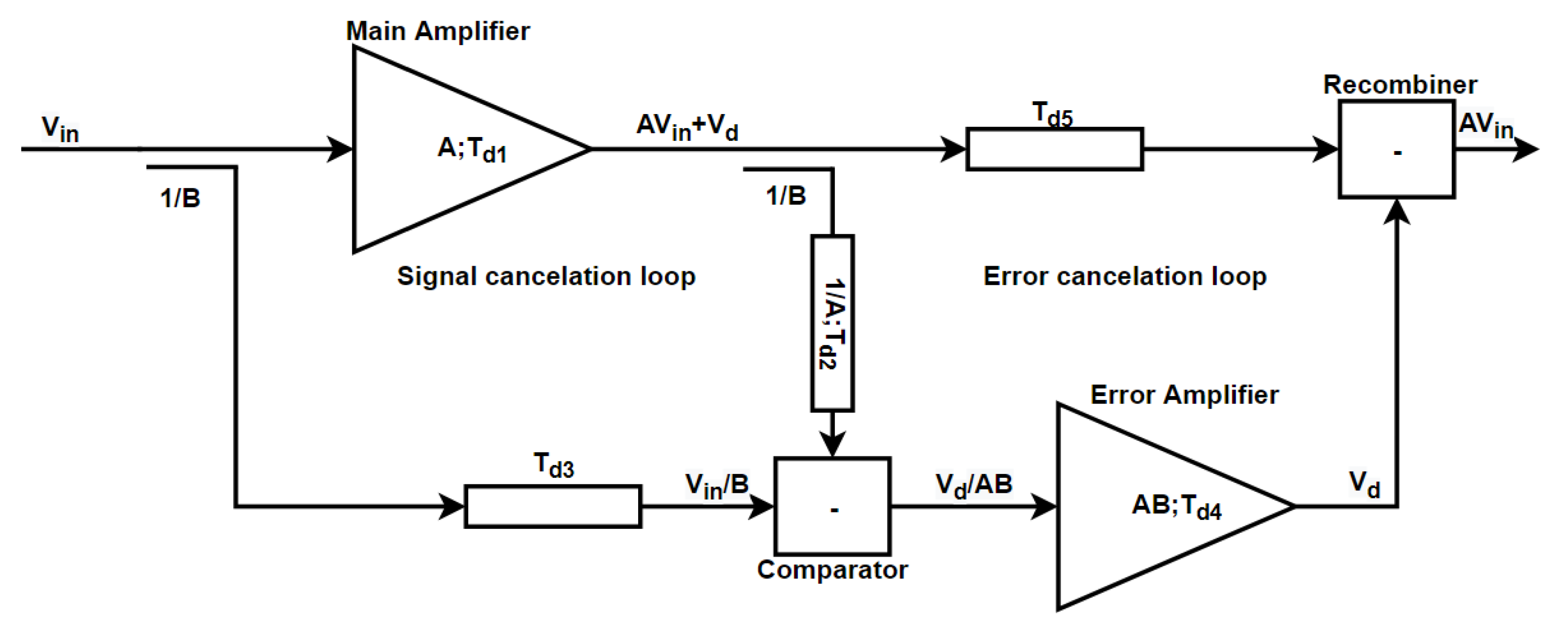
Figure 3.
Simplified feedback operational diagram.
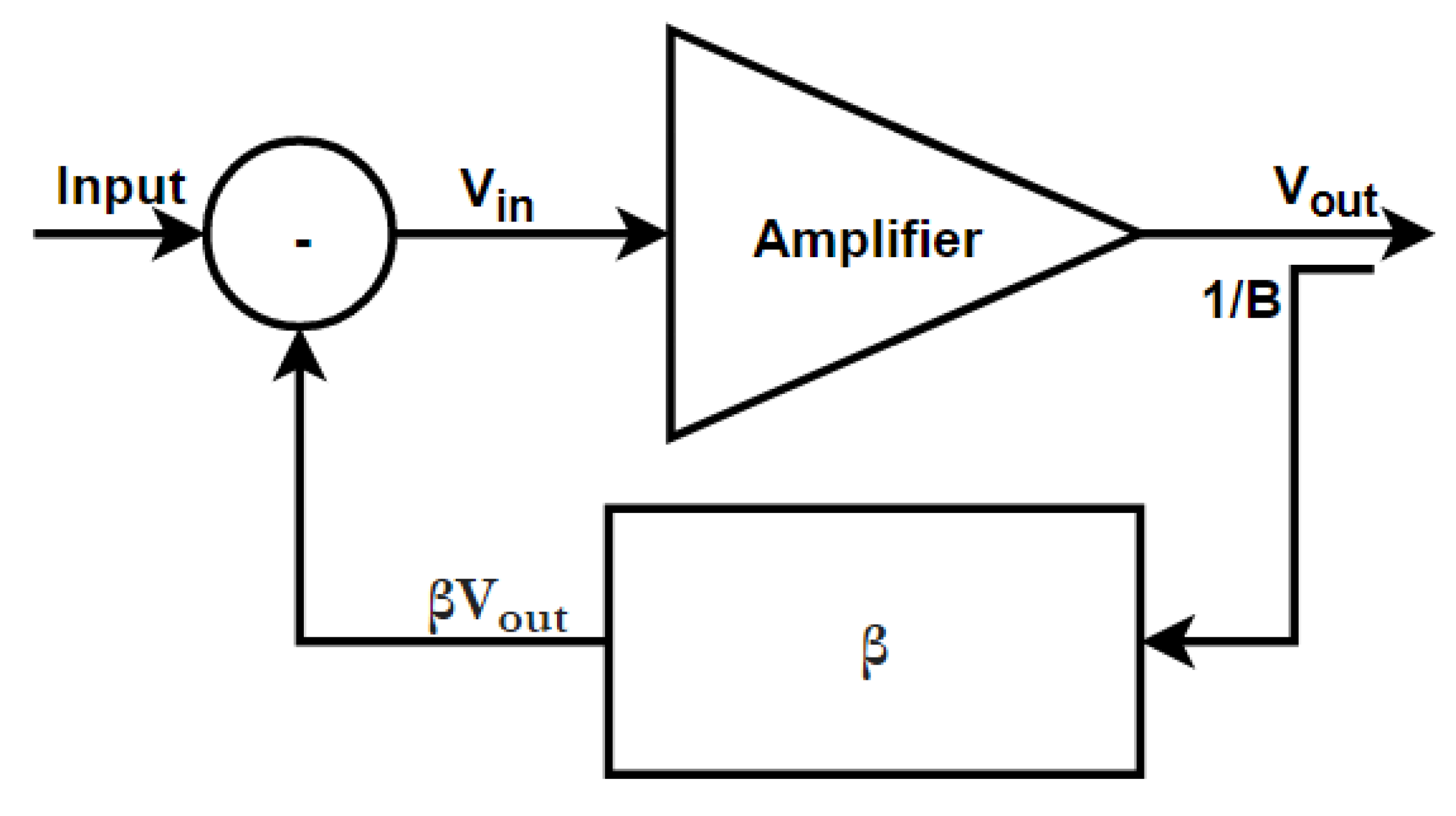
Figure 4.
Active feedback operational diagram.
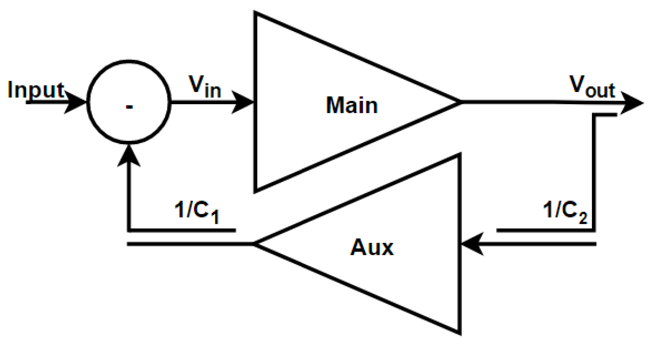
Figure 5.
Envelope feedback operational diagram.

Figure 6.
Polar feedback transmitter operational diagram.

Figure 7.
Cartesian feedback transmitter operational diagram.
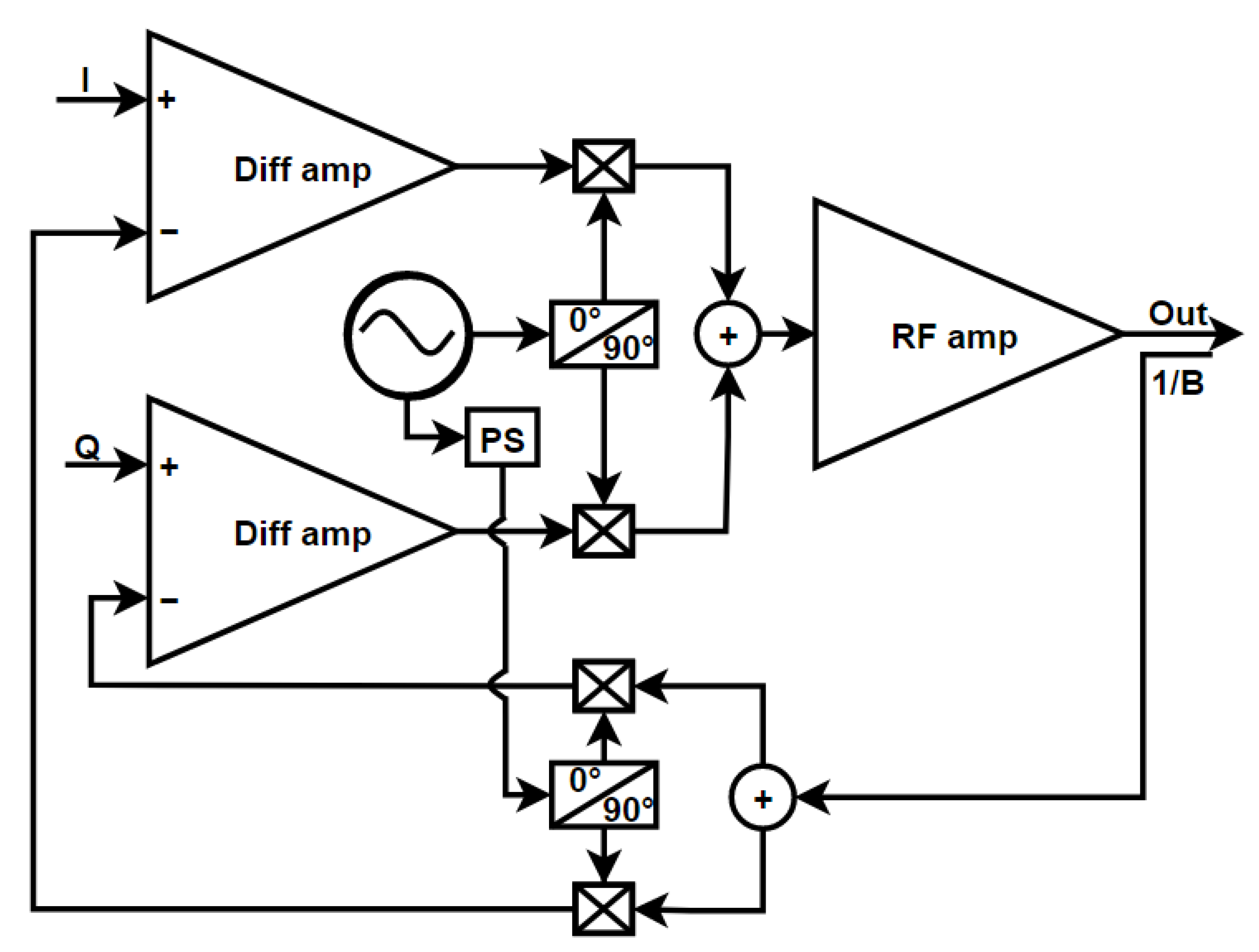
Figure 8.
Predistortion linearization conceptual diagram.

Figure 9.
Adaptive predistortion operational diagram.
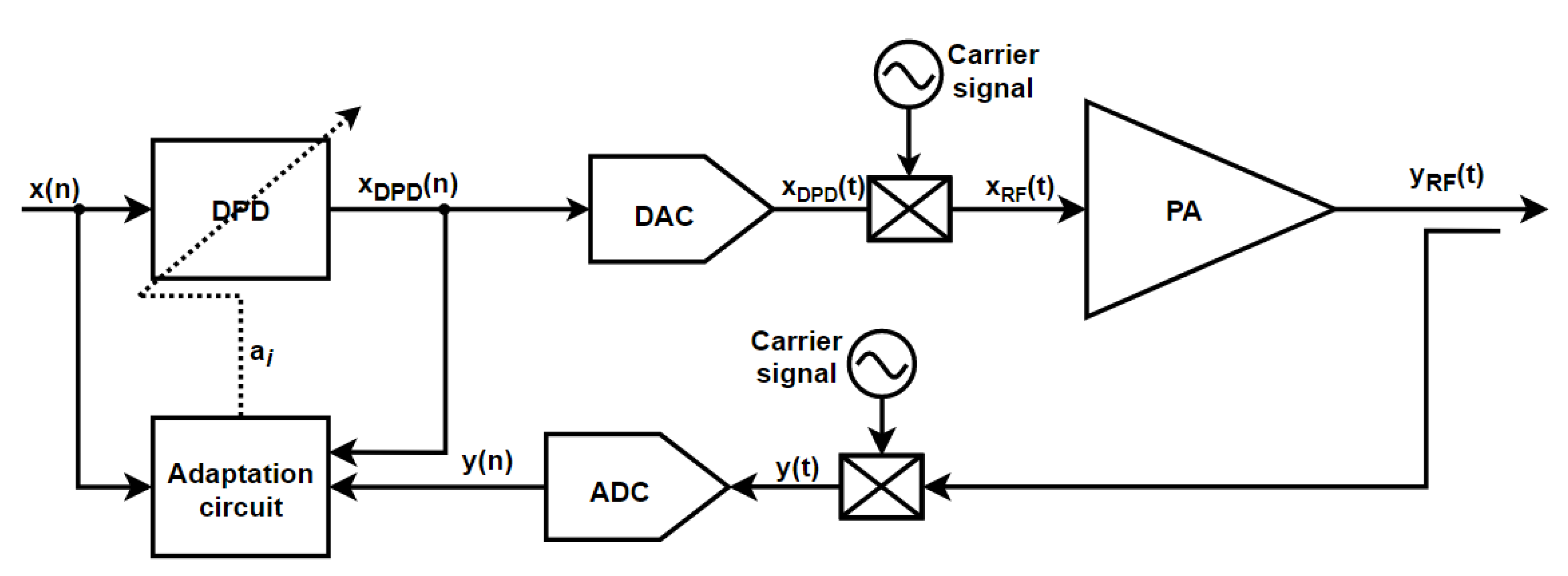
Figure 10.
(a) indirect learning architecture (b) direct learning architecture.

Figure 11.
STR transmitter.
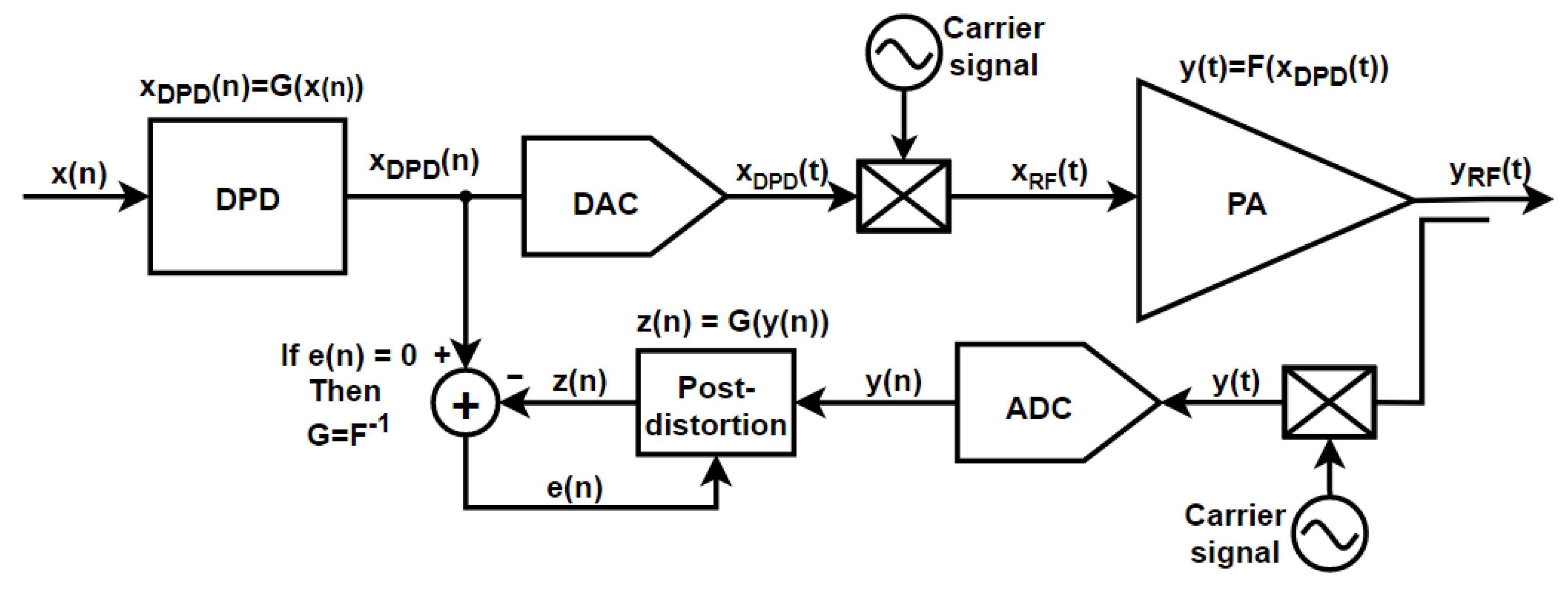
Figure 12.
MRAS transmitter.
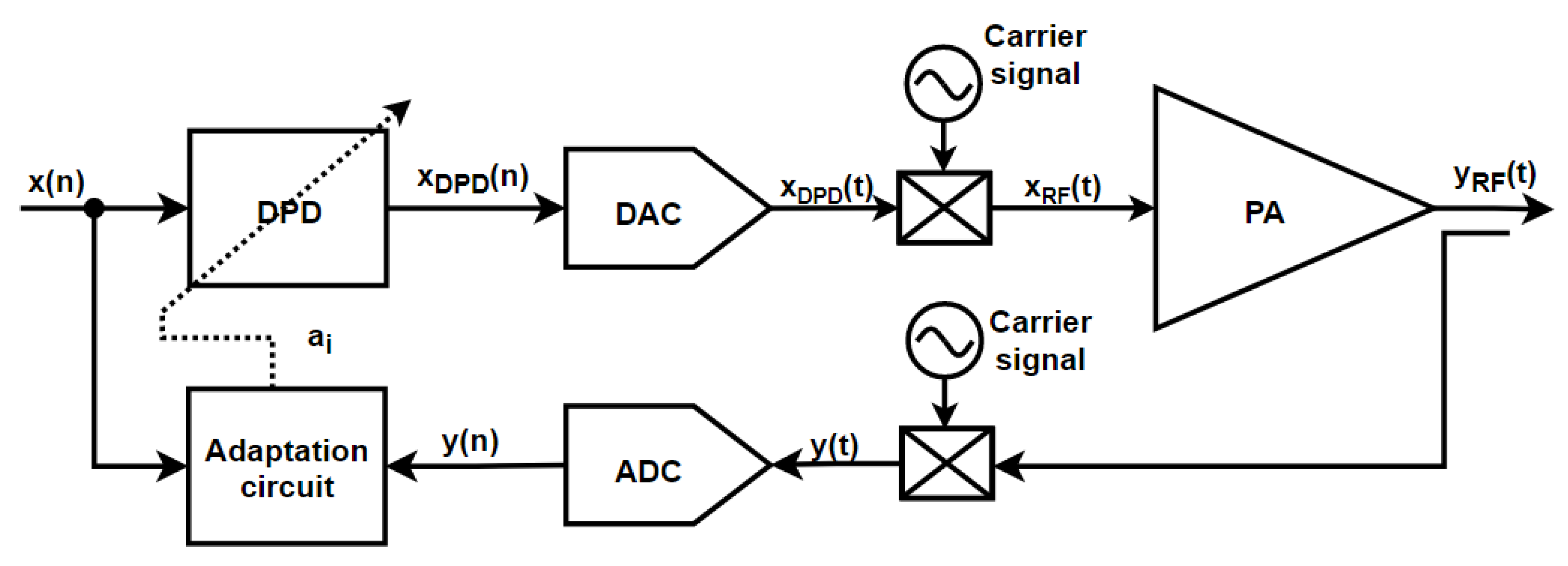
Figure 13.
MRAS-STR transmitter.

Figure 14.
Mixed complex/real transmitter.


Table 1.
Feedforward method results.
| Source | Year | Output Power (dBm) | Efficiency | ACLR (Lowest) dBc | Frequency (MHz) | Test Signal | Bandwidth MHz |
|---|---|---|---|---|---|---|---|
| [14] | 2005 | 44.7 | 10.9% (PAE) | −60.0 | 2140 | WCDMA | 4 |
| [15] | 2009 | 49 | 27.2% | −53.5 * | 945 | Two tone | N/A |
| [16] | 2010 | 43 | 19.4% (PAE) | −53.2 | 2140 | WCDMA | 20 |
| [17] | 2013 | 52.7 | 25.0% | −62.0 | 880 | WCDMA | 10 |
| [18] | 2015 | 51.4 | 21.4% | −63.0 | 880 | WCDMA | 10 |
* Calculated from data.
Table 2.
Feedback method results.
| Source | Year | Output Power (dBm) | Power Efficiency, % | ACLR (Lowest), dBc | Frequency (MHz) | Test Signal | Band-Width, MHz | RF Transistor Technology |
|---|---|---|---|---|---|---|---|---|
| [48] | 2010 | 15 | 13.2 * | −38.4 | 2000 | 64 QAM | 10 | 130 nm CMOS |
| [35] | 2012 | 27.1 | 28 (PAE) | −40 | 1880 | WCDMA | 5 | 130 nm CMOS |
| [43] | 2015 | 16.6 | N/A | −33.8 | 2400 | 16 QAM LTE | 1.4 | 130 nm CMOS |
| [44] | 2017 | 14.1 | N/A | −35 | 2 | 16 QAM | 2 | 65 nm CMOS |
| [46] | 2019 | 21.4 | 22.3 | −49 | 10000 | WCDMA-UL | 4 | 65 nm CMOS |
* Evaluated or calculated from data.
Table 3.
Predistortion results.
| Source | Year | Output Power (dBm) | PAE, % | ACLR (Lowest), dBc | Frequency (MHz) | Test Signal | Bandwidth, MHz | RF Transistor Technology |
|---|---|---|---|---|---|---|---|---|
| [74] | 2010 | 15 | 51 | −42 | 880 | EDGE | 0.2 | HEMT |
| [75] | 2020 | 26.3 | 18.7 (η) | −40 | 900 | 64-QAM | 200 | GaN-HEMT |
| [76] | 2015 | 37.5 | 45 | −48,1 | 1890 | 2-carrier LTE | 40 | N/A |
| [77] | 2013 | 23.3 | 8 | −43,5 | 1950 | LTE | 5 | 65 nm CMOS |
| [78] | 2017 | 46 | 34.6 | −40 * | 2140 | LTE | 20 | LDMOS |
| [79] | 2016 | 35 | 29.8 | −45.9 | 2650 | OFDM | 16 | GaN-HEMT |
| [80] | 2017 | 16.4 | 15.2 | −28.8 | 15,000 | 64-QAM | 200 | SOI CMOS 45 nm |
| [81] | 2019 | 9.8 | 18.2 | −30 | 28,000 | 64-QAM | 340 | CMOS 65 nm |
| [82] | 2011 | 7 | N/A | −21 * | 60,000 | Two tone | 5 | CMOS 90 nm |
* Calculated or evaluated from graphical data.
Table 4.
Linearization methods summary.
| Feedforward | Adaptive Feedforward | Cartesian Feedback | Polar Feedback | Analog Predistortion | Digital Predistortion |
|---|---|---|---|---|---|
| ACLR improvement, dBc | |||||
| 20–24 | 28 | 8–14 | 10 | 6–17 | 3–16 |
| Energy efficiency, % | |||||
| 10–27 | 25 | 13–22 | 28 | 15–18 | 8–51 |
| Bandwidth, MHz | |||||
| 4–20 | 10 | 1–10 | 5 | 200–340 | 1–200 |
| Disadvantages/difficulties | |||||
| Additional power amplifier, dependency on stable operational conditions | Additional power amplifier, additional loop control circuit | Limited bandwidth, additional IQ converters, IQ imbalance, severe bandwidth–gain trade-off, | Additional and expensive phase control circuitry, different amplitude, and phase components spectra | Dependency on stable operational conditions, limited linearization capability | High energy consumption, expensive converters |
| Advantages | |||||
| Relatively high improvement in linearity, relatively high bandwidth | High linearity improvement, high tolerance to change in operational conditions | Improvement in stability conditions over classical feedback, no need of phase locked loop controllers, similar signal component bandwidth, feedback architecture allows self-regulation | Constant amplitude architecture allows us to soften amplifier linearity requirements, feedback architecture allows self-regulation | Relatively easy to implement, possibility to implement at extremely high carrier frequencies and bandwidths | Relatively easy adaptation implementation, versatile architecture |
| Output power level, dBm | |||||
| 43–51 | 52 | 14–21 | 27 | 7–26 | 15–46 |
Publisher’s Note: MDPI stays neutral with regard to jurisdictional claims in published maps and institutional affiliations. |
© 2021 by the authors. Licensee MDPI, Basel, Switzerland. This article is an open access article distributed under the terms and conditions of the Creative Commons Attribution (CC BY) license (https://creativecommons.org/licenses/by/4.0/).
Share and Cite
MDPI and ACS Style
Borel, A.; Barzdėnas, V.; Vasjanov, A. Linearization as a Solution for Power Amplifier Imperfections: A Review of Methods. Electronics 2021, 10, 1073. https://doi.org/10.3390/electronics10091073
AMA Style
Borel A, Barzdėnas V, Vasjanov A. Linearization as a Solution for Power Amplifier Imperfections: A Review of Methods. Electronics. 2021; 10(9):1073. https://doi.org/10.3390/electronics10091073
Chicago/Turabian StyleBorel, Andžej, Vaidotas Barzdėnas, and Aleksandr Vasjanov. 2021. "Linearization as a Solution for Power Amplifier Imperfections: A Review of Methods" Electronics 10, no. 9: 1073. https://doi.org/10.3390/electronics10091073
Note that from the first issue of 2016, this journal uses article numbers instead of page numbers. See further details here.