
Challenges of Overcoming Defects in Wide Bandgap Semiconductor Power Electronics


Materials Science Department, University of Maryland, College Park, MD 20745, USA
*
Author to whom correspondence should be addressed.
Electronics 2022, 11(1), 10; https://doi.org/10.3390/electronics11010010
Submission received: 21 November 2021
/
Revised: 7 December 2021
/
Accepted: 17 December 2021
/
Published: 22 December 2021
(This article belongs to the Special Issue GaN-Based Power Electronic Devices and Their Applications)
Abstract
:The role of crystal defects in wide bandgap semiconductors and dielectrics under extreme environments (high temperature, high electric and magnetic fields, intense radiation, and mechanical stresses) found in power electronics is reviewed. Understanding defects requires real-time in situ material characterization during material synthesis and when the material is subjected to extreme environmental stress. Wide bandgap semiconductor devices are reviewed from the point of view of the role of defects and their impact on performance. It is shown that the reduction of defects represents a fundamental breakthrough that will enable wide bandgap (WBG) semiconductors to reach full potential. The main emphasis of the present review is to understand defect dynamics in WBG semiconductor bulk and at interfaces during the material synthesis and when subjected to extreme environments. High-brightness X-rays from synchrotron sources and advanced electron microscopy techniques are used for atomic-level material probing to understand and optimize the genesis and movement of crystal defects during material synthesis and extreme environmental stress. Strongly linked multi-scale modeling provides a deeper understanding of defect formation and defect dynamics in extreme environments.
1. Introduction
One of the most significant challenges for materials technology in the 21st century pertains to the excited state characteristics of crystal defects present in semiconductor and dielectric materials used for energy conversion devices [1,2,3,4]. These high-voltage and high-power switching devices experience extreme electrical and thermal stresses because of inherent high electric fields and high currents generated during their operation. In addition, they are subjected to extreme environments, including high ambient temperatures, thermal cycles, high magnetic fields, radiation, vibration, and corrosion.
Silicon has served well as the industry “workhorse” semiconductor for power electronics switching applications; however, wide bandgap (WBG) semiconductors, especially diamond and GaN, with significantly superior electrical and thermal characteristics compared to silicon, are the key enablers for transforming the electricity infrastructure for the 21st century [3,4,5,6]. Current filament formation and micro plasma generation are the main causes of power semiconductor device failures in circuit applications. Device failures occur either during the on-state when conducting high amounts of currents or when switching high voltages and currents. There are significant experimental test results suggesting that material defects in WBG semiconductors and diamond severely limit the manufacturing yield, device performance, and long-term field reliability, thereby hindering many of the key beneficial attributes of WBG and ultra-wide bandgap power semiconductor technology for advanced energy initiatives. These performance and reliability limitations in WBG power switching technology severely impact future advances in many of the commercial applications, including vehicle electrification, utility grid transformation, and renewable energy utilization.
This review concentrates on the elements which limit the present-day wide insertion of these technologies in power electronic applications. The present study shows that what is lacking is the fundamental understanding of the role that crystal defects play when WBG semiconductor devices are operating under extreme temperature and voltage environments. For example, it is not clear if certain types of defects are benign, and if they are, then for how long. This basic understanding of the genesis and excited state behavior of crystal defects is critical to (1) study and quantify the role of specific type of defects on the performance and reliability of WBG high-voltage devices, and (2) devise appropriate material synthesis and device fabrication techniques that yield reduced defect density and mitigate the deleterious effects of defects.
The present investigation has focused on material behavior in the extreme environment. The basic experimental and theoretical research on the physical phenomena relevant to defects in the WBG semiconductor and diamond materials used in high-voltage power-switching devices as well as the high temperature environment are presented. The application of advanced material probing techniques is presented for the real-time study of defect dynamics when WBG semiconductors and diamond are subjected to extreme environmental stress.
The defects degrade the expected material theoretical properties. At present, electrical devices, components and subsystems categorically rely on materials that appear or behave in ways that are very different from ideal. Evidence suggests that defects in real technologies have been heretofore unavoidable because of conditions in growth and the processing of materials long before their integration into actual devices.
Although defects are manifested in the electrical performance of a device, two potential routes were pursued for reducing their effect, corresponding to two overarching scientific questions. (1) Can we understand the origins, evolved forms, and dependency on extreme conditions of individual and agglomerations of defects in a manner that promotes their manipulation and annihilation? (2) How does this information ultimately influence the electrical properties and performance of the materials and devices in extreme environments? The response to the first question is to identify and eliminate the root cause, namely, the lattice defect itself as it originates at interfaces, surfaces, and bulk regions [7,8,9]. This is a problem of manipulating the material structure as the material is being synthesized. Through careful design of growth conditions, it may be possible to develop lattice features that inhibit the nucleation or propagation of defects. The second potential route is to ameliorate the effects on the electrical performance of the lattice defect by exploiting the fundamental behavior of electrons in the presence of defects. Significant additions to the state of knowledge are still needed to effectively pursue either of these routes. In fact, the effects caused by the extreme conditions to be experienced by the lattice and electrons and scientifically sound approaches to deal with the associated challenges are still elusive. High temperatures, large electrical or magnetic fields, radiation sources and mechanical stresses bring about complications that break conventional rules based on idealized conditions.
Computational simulations have a unique but complementary role in these pursuits. They can be used to limit the number of active theoretical parameters and control their influence on a mechanism, thereby eliminating the effects of variables that may be difficult to isolate in some experiments. Computations can also allow us to limit the complex material synthesis experiments necessary to achieve low dislocation densities. This can be used to identify parameter dependencies that are most influential over the response variables of interest. In this regard, computational methods and simulations can work as tools for true scientific discovery by delivering numerical solutions to theoretical equations whose parameters and conditions are so complex that they would not be solved otherwise. Computing-based test beds can also be used to develop important new ideas to screen and design novel experiments. This can ultimately promote focus on feasible concepts, thereby enabling an accelerated pipeline to commercialization and adoption. Computations are enabled, in large part, by new algorithms that make it possible to investigate defects at varying scales of description that were intractable just five years ago. Moreover, the ever-increasing capabilities of processor technologies also open the possibility for new research directions to develop new modeling theories and techniques to investigate mechanisms that remain inaccessible through existing computing approaches.
The current state of bulk diamond and GaN crystal growth technology lags behind even the state of silicon wafer technology of the 1960s in terms of defect density and cost. Today, diamond and GaN wafers are much smaller than silicon, more than 100 times higher in cost and contain 1000 times more defects than silicon wafers. This situation is not likely to change in the foreseeable future. In summary, while there is evidence that dislocation densities in diamond and GaN bulk substrates have diminished over the past two decades, significant densities of defects persist that will require a very large investment of resources over a sustained period of time before they can be significantly reduced [10,11,12,13]. Research in bulk substrates is beyond the scope of the power electronics industry. Therefore, most of the focus is on using surface modification methodologies to influence defect propagation from the substrate into the epilayer, and to investigate the electrical activity of defects in the epilayer as well as the influence of defects on the epi/dielectric interface.
In the past two decades, much of the federal investment in power electronics in the U.S. has been directed toward applied research focused on demonstrating power converter applications based on wide bandgap (WBG) power devices [14,15,16,17,18]. At the present, commercially available power devices have limited voltage and current ratings, are prohibitively expensive, and are yet to be proven reliable in extreme environment applications [3]. Furthermore, the manufacturing yield is “low”, which is largely due to a high density of material defects in both SiC and GaN semiconductors [19,20].
2. Results from the High Voltage/Temperature Extreme Environmental Evaluation
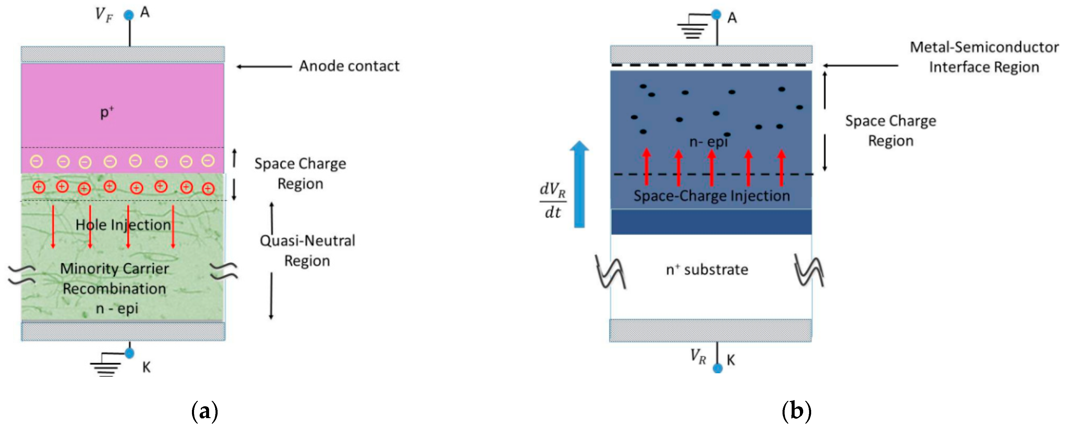
Wide bandgap semiconductor materials experience both intrinsic and extrinsic extreme environmental stresses that are at the limit of material breakdown. For example, the semiconductor and dielectric materials used in the construction of power electronic switching devices experience extreme electrical and thermal stresses during the on-state as well as when switching high voltages and high currents. In a bipolar power semiconductor switching device (Figure 1a), the high-level injection of minority carriers is required to achieve significant conductivity modulation and reduce the on-state resistance. If the semiconductor contains a high density of crystal defects, as is the case with wide bandgap (WBG) semiconductors, minority carrier recombination is adversely affected [21,22]. The basal plane dislocations (BPDs) present in SiC are excited by the energy released from the minority carrier recombination process, which leads to additional BPD generation along with its associated movement within the semiconductor material, causing an increase in the on-state resistance and eventual thermal run-away in a forward biased bipolar junction diode. This finding prompted the “world-wide” research community to investigate new material synthesis techniques that convert BPDs into threading edge dislocations (TEDs) [23,24]. The exact role of TEDs on device performance and reliability, especially under extreme environments, is still not well understood. In a similar development, the space-charge injected during voltage switching in a majority carrier device, such as the Schottky barrier diode (Figure 1b), results in local regions of elevated thermal dissipation or “hot spots” that cause loss of electrical functionality in SiC, even at moderately low dv/dt values (see Figure 2a) [25]. To date, there is no convincing explanation of this physical mechanism, although there is experimental indication showing a correlation between “hot spots” and defects. A fundamental requirement of semiconductor materials in such high-power applications is the ability to withstand localized Joule heating. It was shown that the worst-case Joule heating occurs when the semiconductor power switch is experiencing a simultaneous high-current and high-voltage condition, often referred to as an “avalanche state” [26,27]. This situation typically occurs when the switch is short-circuited and/or absorbing the energy stored in a charged inductor. The measured avalanche energies of 600 V silicon and SiC power diodes are shown in Figure 2b [25]; the silicon diode has more than two orders of magnitude higher avalanche energy than the SiC power diode. This observation is particularly startling since the SiC material is expected to withstand increased Joule heating because of its superior electrical and thermal properties compared to silicon. Similar experimental data for GaN semiconductors are yet to be reported. The measured limited dv/dt and avalanche capabilities of the SiC semiconductor strongly suggest that material defects have a profound impact on its electrical power switching performance under extreme high-voltage and high-temperature intrinsic environments. Since GaN semiconductor has even higher density of material defects (greater than 104 cm−2), this problem may be further exacerbated. A fundamental understanding of the behavior of material defects in WBG semiconductors and dielectrics is critically needed, especially when subjected to extreme environments. An important research result comes from the application of novel scanning force microscope (SFM) and synchrotron X-ray topography for real-time spatial and temporal characterization of material defects when stressed under high electric fields and temperatures. The initial results of the X-ray topography of thick GaN epitaxy (reported by the author) show a dislocation cell structure very different from the previous reported results for other wide bandgap semiconductors.
2.1. Effects of High-Temperature Stress on Metal–Semiconductor Interface
Controlling defects and understanding their effects on electrical properties of semiconductors and dielectrics under extreme environments also includes the metal–semiconductor contacts that provide mechanical support and electrical interconnection for the device, and also remove heat from active semiconductor regions. However, these packaging materials, when improperly chosen or processed, can induce strain into the semiconductors, resulting in defect generation and changes in the electronic transport in the semiconductor. Note that SiC and GaN are particularly susceptible to package-related thermal stresses, which may interact with the semiconductor material residual stresses and even piezoelectric stresses augmented at elevated temperatures.
Metal contacts to the doped semiconductor regions, either ohmic or Schottky, generally remain stable within the envelope of the extreme environment. Establishing a low electrical resistance and a low thermal boundary resistance requires tailoring the metal contacts to minimize electron and phonon scattering, respectively. Furthermore, complex thermally stable thin film contact metallurgy is generally applied to obtain interfaces with high performance electrical, thermal and mechanical characteristics [28]. Ohmic and Schottky contacts for SiC and GaN were extensively studied; however, the long-term durability of multilayer metal contact structures at elevated temperatures up to 500 °C needs to be understood [29,30,31,32,33]. Physical mechanisms, such as diffusion and inter metallic/void formation at elevated temperatures may lead to significant changes in basic mechanical and electrical properties of the contact. Johnson et al. [34,35,36,37] studied the mechanical die shear strength of multilayer thin and thick film metal interfaces for high-temperature environments. Basic material degradation effects, including nano-void formation and evolution, and electromigration were observed.
2.2. Physics of Failure Analysis for Extreme Environment Predictions
The extreme environment, whether temperature, radiation or mechanical stress is the accelerating parameter, provides the perfect condition for degradation (as related to defects). In this effort, the physics-of-failure (PoF) methodology is applied in the present work as the method for degradation data analysis from the extreme environment accelerated tests. The fusion prognostics method of testing, which combines PoF modeling with data-driven prognostics, allows extreme environment tests to be terminated before failure, significantly reducing the test time, and to be able to capture the intended physical phenomenon prior to complete degradation. The loading conditions include the complex multiple environments of temperature, temperature cycling, high fields and radiation stresses (see Figure 3).
2.3. Evaluation under Extreme Radiation Environment
The basic understanding of defect generation and interaction with the radiation environment is based on single event charge deposition and trapping, and the total dose radiation and ionizing radiation dynamics on test structures, such as MOS capacitors and diodes (Schottky and PiN diodes). The results were incorporated into radiation materials physics models in conjunction with Monte Carlo simulations for channel transport, transport in the presence of single-event deposition processes as well as total dose deposition. The investigations were able to attain a clear basic science understanding of the interactions of the radiation environment with defects and electrical transport in GaN and SiC semiconductors.
The most important single event effects (SEE) are the classical single-event upset (SEU) and the lesser known but increasingly important digital single-event transients (DSET). Unlike SEU, DSET events give rise to charge transients, which propagate to interfaces and further upset the charge distribution at the interfaces. Several criteria must be met for a DSET to result in material degradation: (a) a path must exist from the struck node to a metallic drain, or a transient of charge must be of sufficient magnitude and width; and (b) the transient must arrive with an appropriate delay time. The present research investigates neutron interactions with GaN and SiC bulk materials and their surfaces and interfaces. We initially showed that neutrons introduce defects at interfaces, which decrease the net polarization charge as well as the free electron concentration in channels. The identified shallow trap exhibits donor-like behavior. At fluencies above 1014 n/cm2, an impurity band is formed, and the conduction mechanism becomes thermal. Carrier removal due to neutron interactions is also a significant observation in the present work. The issue of ionizing radiation is due to the extreme space environment from cosmic radiation, which results in positive charged particles and Van Allen belts, which produce energetic electrons and protons. Solar radiation produces gamma radiation and protons. The cumulative long-term ionizing damage due to proton, γ- and β-radiation results in a total ionizing dose which raises the semiconductor to an excited state, resulting in yet unexplored phenomenon, such as phonon accumulation.
2.4. Accelerated Stress Testing to Quantify Cosmic-Ray Induced Failures
The critical environment effects of cosmic radiation were made evident by the reported failure of silicon power devices in space and high-altitude applications [38]. Although fewer and lower energy cosmic rays reach the Earth’s surface, this phenomenon is an increasing concern for terrestrial applications of power semiconductor devices. Studies have shown that cosmic-ray-induced effects can strongly influence the voltage de-rating necessary for the safe and long-term use of silicon power devices, directly affecting their adoption and use in various applications. The high energy particles in cosmic rays are known to damage high-voltage silicon power devices, resulting in single-event upsets (SEUs), such as single-event burnout (SEB) and single-event gate rupture (SEGR). The SEB is caused by the initiation of destructive avalanching, due to drain-source current filaments resulting from the activation of parasitic bipolar elements present in all power devices, except diodes. The SEB in diodes is simply due to excessive leakage current induced by high-energy particles while the device is biased at a high voltage. In MOS-controlled power devices, SEGR can occur due to the generation of a high transient electric field across the gate oxide and subsequent discharge of accumulated holes through the gate oxide. Consequently, silicon power devices are limited to approximately 50% of their rated voltage in characteristic usage [29]. The challenge is then to carefully investigate the interaction of material defects in SiC and GaN structures with the cosmic rays [39].
2.5. Defect Spectroscopy
The techniques reported include deep level transient spectroscopy (DLTS), photoconductivity spectroscopy, photo-induced current transient spectroscopy (PICTS) and photoluminescence spectroscopy. Optical defect spectroscopic techniques are especially useful for WBG semiconductors since they can access a wide range of defects with energies deep within the bandgap, not accessible by thermal ionization. Furthermore, these techniques can detect defects as low as the part per billion level; in addition to determining the defect energy level, the concentration and capture cross-section were determined. Defect formation by irradiation was previously studied in detail for GaN materials and devices [40]. Irradiation results in carrier traps that reduce mobility and conductivity. A number of traps due to native defects and complexes were previously identified by DLTS. For SiC devices, the irradiation of Schottky barrier diodes (SBDs) with γ-rays and electrons were undertaken [41,42].
3. Intrinsic Electrical and Thermal Stresses
Perhaps the most important stressful environment that a power semiconductor material undergoes is when it is operating in a real high-voltage circuit environment [29]. These types of structures behave like classical high-voltage switches and are referred to as “power switches”. Because of basic electrical and thermal material properties, SiC and GaN “power switches” generate very high internal temperatures as well as voltages, and in addition, may be operated at much higher temperatures and at increased switching speeds compared to similar silicon power switches. The intrinsic electrical and thermal stresses are further magnified by external extreme environments; the main intrinsic stresses are as follows.
3.1. On-State Static Electrical Stress
Typical power semiconductor devices are operated in the on-state (a state of high current density) for nearly half the time during their lifetime [30]. In the on-state while conducting a large current, the bulk semiconductor material is significantly heated due to Joule heating, whereas the MOS junction experiences charge accumulation and eventual dielectric breakdown. Future research will separately employ constant-voltage and constant-current electrical stresses [43] to low-voltage MOS junctions and high-voltage Schottky and PiN diodes and monitor the junction electrical characteristics and defect behavior using advanced in situ defect probing techniques. The tests should be conducted at various junction temperatures up to 300°C until failures occur, the failed parts being probed to identify the cause of failures, especially in the study of the role of various types of material defects.
3.2. Off-State Static Electrical Stress
In the off-state when the power semiconductor device is blocking high reverse-bias voltage, a space-charge region is created within the semiconductor bulk material [29]. The space-charge region is formed within the lightly doped epitaxial semiconductor material, which contains a high density of crystal defects. Although the static current flowing is small and is mainly due to space-charge generation and recombination, a high electric field exists across much of the space-charge region. At the present time, the defect characteristics in this excited state are not understood. Future investigations must be focused on obtaining a fundamental understanding of the role that various types of crystal defects play on the reverse blocking characteristics of SiC and GaN materials over a prolonged period. The failed test structures should be probed to identify the cause of failures, and especially the impact of various types of material defects.
3.3. High-Voltage and High-Current Switching Stress
It has been known for quite some time that the most catastrophic failures in power semiconductor devices occur during the switching of high voltages and high currents. An extremely stressful condition involving a simultaneous high-voltage and high-current situation occurs when an electrical load is short-circuited and/or when switching a charged inductive load in real circuit applications [44]. This condition is typically referred to as “avalanching” and results in excessive power dissipation within a very short time. Another extremely stressful event occurs when switching a high voltage electrical load, even when the steady-state current flowing is very small. This condition leads to a very high dv/dt across the power semiconductor switch, which will result in the injection of a large amount of space charge within the reverse-biased semiconductor material subjected to a high electric field. Both the dv/dt and avalanche capabilities of SiC and GaN semiconductors were shown to be orders of magnitude smaller than those of the silicon semiconductor [25,26,27]; however, a fundamental understanding of the role of high density of crystal defects in SiC and GaN semiconductors when subjected to these extreme environments is lacking. Specialized test circuits to apply controlled dv/dt, short-circuit, and avalanche stresses on packaged high-voltage diode test structures at various ambient temperatures up to 300 °C must be developed and appropriately tested. By varying the stress conditions until destructive failure occurs, the exact location of the failure may be detected using material analyses including SEM, HRTEM, and X-ray techniques. These expected experimental results may be used to validate the condensed matter physics of excited defect states under extreme environments and to develop compact physics-based models for defect dynamics.
The combination of intrinsic and extrinsic stresses places significant limits on the material’s “safe operating region”. The important measure of the safe operating region of a semiconductor material can be defined in terms of the same semiconductor material but in a “power switch” configuration through the device’s safe-operating area (SOA) [29]. The SOA refers to the amount of electrical energy that a power semiconductor device can reliably switch in an actual circuit application when operating under extreme environments.
The expected SOA of SiC and GaN power devices is shown in Figure 4. It is a function of the net material defect density (Dit), switching current density (Jon) and the maximum junction temperature (Tjmax); it is also a function of the ambient temperature (Ta), switching duty ratio (D), and the switching dv/dt and di/dt.
3.4. Electron Transport under High Magnetic Field Stress
While much is known about electron transport in GaN and SiC at low magnetic fields, little is known about transport at high magnetic fields. At high magnetic fields, the band structure is modified by the Zeeman effect and spin-orbit coupling. This modification in turn affects the electron transport properties, including effective mass, mobility, and scattering time. This also affects the high field magnetoresistance. Interface states and interface roughness are believed to limit the channel mobility. Considerable progress was made in the fabrication of MOSFET devices in SiC and GaN [30,31,32]. Deep level transient spectroscopy (DLTS) may be used to measure electronically active interface states. Electron transport in these structures are measured in magnetic fields up to 15–18 Tesla. Although the magneto-transport properties of narrow gap III-V materials and devices [32] were reported, such information is not available for wide bandgap semiconductors. In such an investigation, both longitudinal and transverse magnetoresistance may be measured over the temperature range of 4 to 300 K. The carrier mobility must be determined from the Hall effect as a function of magnetic fields. From the electric and magnetic field dependence as well as temperature dependence of the mobility and magnetoresistance, scattering mechanisms may now be determined at low and high fields, compared to theory [33,34,35,36]. The channel electron mobility at high magnetic fields as a function of charge density and interface roughness can be measured and analyzed as well as the channel mobility for materials with different dislocation densities.
4. Material Theory and Simulation
A very necessary approach can potentially integrate materials synthesis and extreme environmental evaluation, using multi-scale modeling to provide first principle understanding of (1) defect growth and evolution during deposition of an epilayer and (2) defect growth and propagation because of extreme environment evolution. The building blocks for materials in extreme environment simulations then can focus on the theme of “indirect stochastic influence” as a means to control electrons and atoms.
4.1. Defects with Atomic Resolution at Interfaces and Surfaces
Previous efforts to calculate the basic physical properties of SiC and GaN showed that modern atomistic methods can be employed effectively to study crystal defects. SiC was studied more exhaustively than GaN in these atomic-scale simulations. For instance, defect configurations and band structures were computed [37], induced gap states were calculated through semiempirical techniques at interfaces [38], and excited states were predicted for the numerous polytypes of SiC through quasiparticle techniques [37]. In contrast, a relatively smaller number of computational investigations were undertaken for GaN defects. Results such as core configurations [45,46] and excited states [38,39] only began appearing in the last decade. Although GaN has a large direct gap of 3.4 eV and a high breakdown field of 5 × 10⁶ V/cm, it is limited by the large density of threading dislocations (TDs), which can reach surface densities greater than 1010 cm−2 [47]. Threading screw dislocations (TSDs) in both GaN and SiC can induce electronic states deep in the band gap and alter the performance of the devices. It is well known that certain configurations of these dislocations exist, but open questions remain about the detailed core atomic structures. Controversy surrounds the location of the core relative to the positions of the Ga and N atoms in the lattice. Without knowing the accurate core structure, precise electronic structures originating from dislocations cannot be determined because the electronic properties of dislocations strongly depend on the atomic configuration in the core.
Computationally efficient models to study the structure and formation energies of point and extended defects were developed by Bellotti [40,48]. The calculations were based, in part, on generalized Kohn–Sham DFT. Bellotti showed that an open core type dislocation in GaN was obtained, as shown in Figure 5 [40]. The most stable core structure in the Ga-rich limit is the “A” Ga-filled core, where only Ga atoms exist around the core. However, in the N-rich limit, the most stable core configuration is the “B” open core, where both Ga and N atoms are removed from the core. In this case, the hollow type “B” open core and 8/5-member ring type can co-exist.
4.2. Accurate Electronic Structure and Excited States of Defects
The simulation of defects in excited states was reported by Bellotti and Grein. TSDs in GaN grown in Ga-rich conditions are electrically active and detrimental to electronic properties (e.g., current leakage [41,42]). Recently, electrically inactive GaN samples grown in N-rich conditions were reported. In these samples, reverse bias current leakage is absent [49]. This result cannot be explained by previous theoretical models, which show electrical activity regardless of growth conditions [50]. Using such newly discovered core structures, as seen in Figure 6, it is possible to determine which cores are energetically most stable in N-rich conditions and determine the influence of the structure on the electric behavior [43].
4.3. Interface Interactions with Dislocations
Density functional theory (DFT) is also able to accurately predict ground state properties and atomic configurations of crystalline defects [50]. To estimate excited-state density requires methods beyond standard DFT, such as hybrid functional or GW approximation. However, the increased accuracy offered by such approaches brings about greater computational costs. This limits simulations to sizes smaller than the typical distances seen between crystalline defects in experiments. Defects may also evolve dynamically and, as a consequence, their configurations and properties vary with time. For such situations, dynamic approaches [44,51] may be used to solve for the trajectories using accurate force calculations based, for example, on DFT or GW. However, the relatively large computational cost required makes it difficult to extend high accuracy approaches to condensed matter physics. Thus, atomic arrangements of dynamically evolving defects are best studied using methods in which the force calculation is relatively inexpensive.
Interfaces between the substrate and the epilayer are a major source of defects. The defects originate from pre-existing defects in the substrate materials and are promoted by stresses from the lattice mismatch effects (Figure 6) [51]. The formation of the TDs is affected by the different terminating atomic species at the substrate step; it is expected that interfacial structures, interfacial ad-atoms, additional buffer layers, or stresses will also change the defect configurations. To achieve control over defect content and configurations in semiconductor materials, the defect interactions at and near interfaces must be understood. The knowledge of defect interactions with interfaces gained here serves as a basis for examining pre-treatment of the substrate surfaces as a means to reduce the number of defects during growth (see Figure 7) [52,53,54].
Dislocations move under the action of forces arising from strain fields experienced during epitaxy, elevated temperatures, high electric and magnetic fields, and interactions with other defects. It is inevitable that the dislocations will entangle with one another as a result of any movement, forcing so-called reactions to occur that lead to the locking of segments that transform glissile dislocations into sessile dislocations [45]. Sessile locks become obstacles for other moving defects that can collide, react, and multiply further. Thus, knowledge of defect mobility is a fundamental building block for top-down material design when dislocation multiplication needs to be controlled.
5. Defects in the Epitaxial Layer
5.1. Impact of Defects on Electron Transport
Carrier dynamics in semiconductors are comprised of long periods of electron-free flight interrupted by scattering events due to phonons and other electrons. Since the scattering events and duration of flights follow random distributions, full-band Monte Carlo methods may be used to model the transport if the band structures are known. Past experience with silicon has shown the accuracy of this approach for predictions of device performance [46]. These methods must be further developed to investigate device mechanisms, such as electron- and hole-initiated multiplication gain and breakdown voltage in SiC and GaN structures [55].
Christou et al. reported that defect evolution is critical in the performance of vertical GaN MOSFETS, where the n-type epitaxy is greater than 10 microns [56]. Dislocations propagate during epitaxy and, in the case of TSDs, they also alter the morphology of the films by inducing spiral growth, which leads to mound structures, even in vicinal surfaces, where the growth mode a priori is dominated by step flow. However, not all the TDs make it through the epitaxial process. Experimental evidence indicates that macro steps can deflect TDs away from the surface during epitaxial growth [52], leaving possibly mixed-type stacking faults on the basal plane [57]. One possible mechanism entails macro step overgrowth of the surface outcrops [58]. This is an important potential approach to eliminating dislocations by turning them before they can reach the open surface. However, the conditions that affect the turning must be better understood. Reductions in the TD density were observed to be as large as two orders of magnitude in SiC [59]. However, the turning must not be at the expense of additional defects of other types [60], particularly if they may further degrade the electronic properties despite the reduction in TD density. At the core of this issue is the very fundamental question of understanding the interplay between the growth conditions, the role of macro step-induced deflection, and the overall dynamics of TDs during epitaxy. Two key external factors are the role of the substrate (i.e., crystal orientation and miscut) and the role of the precursor–surface interactions. Figure 8 indicates that through X-ray topography, a dislocation cell structure may be identified in thick epitaxial layers grown directly on bulk GaN substrates.
5.2. Defect Evolution under Stresses and Large Temperatures
Half-loop arrays (HLA) are generated as a result of the interactions among basal plane dislocations and the growth surface [62]. HLAs form when a primary segment on the basal plane glides as a result of the stresses near the free surface and lays seeds that, with continued growth, turn into the half loops [49,60,63,64]. By careful design of factors that affect the configurational forces, the primary gliding basal plane may be held fixed. Or more generally, a stress environment may be created that favors dislocation obviation or elimination processes. Discrete dislocation dynamics approaches have proven useful in modeling these forces and subsequently studying the resulting dynamics of large ensembles of dislocations and shown in Figure 9. While single dislocation mechanisms and forest effects in SiC and GaN can be modeled with discrete dislocation dynamics methods, as depicted in Figure 9, plasticity is not a main concern.
5.3. Defects in GaN and Related Compounds
It is well known that III-N materials suffer from both extended and point defects, each of which challenge the material’s use in energy applications. Extended defects include vertical threading dislocations of both edge and screw type. The latter defects were shown to be correlated with leakage in vertical two-terminal device structures, while the influence of the former is still undetermined and remains a critical research issue [65]. These extended defects occur in all epitaxial layers grown on c-plane substrates (the predominant and largest area substrate type) and are the result of the lack of a high-quality substrate bulk material, as well as substrate surface. Even in the best current substrate technology, low-defect seeds are scarce [66]. Point defects influence the background carrier concentration in low-doped layers and various recombination processes. The nature of III-N materials makes nitrogen vacancies a predominant point defect that automatically dopes the crystal n-type; however, there are impurities (oxygen and carbon) from most growth environments that also contribute to conductivity. These defects are not well understood and not well controlled. Such defects must be minimized so as to realize drift regions that support both high blocking voltages and low ON-state resistances.
6. Summary
The review of the role of crystal defects in wide bandgap semiconductors and dielectrics under extreme environments (high-temperature, high electric and magnetic fields, intense radiation and mechanical stresses) found in power electronics was presented and is summarized in Table 1. Understanding defects in such semiconductors is necessary in order to realize the enormous potential for advanced energy applications. Material synthesis and characterization techniques with atomic-level control are necessary in order to achieve dramatic reductions in bulk and interface defects needed for materials operating within these extreme environments. This will require real-time in situ material characterization during material synthesis and when the material is subjected to extreme environmental stress. It is shown the reduction of defects represents a fundamental breakthrough that will enable semiconductors and, namely, wide bandgap (WBG) semiconductors, to reach full potential. The main emphasis of the present review was to understand defect dynamics in WBG semiconductor bulk and at interfaces during the material synthesis and when subjected to extreme environments. High-brightness X-rays from synchrotron sources and advanced electron microscopy techniques were used for atomic-level material probing to understand and optimize the genesis and movement of crystal defects during material synthesis and extreme environmental stress. Strongly linked multi-scale modeling also provides a deeper understanding of defect formation and defect dynamics in extreme environments.
Author Contributions
Conceptualization, A.C.; methodology, A.C.; validation, A.C. and B.S.; formal analysis, A.C.; investigation, A.C. and B.S.; resources, A.C.; data curation, B.S.; writing—original draft preparation, A.C.; writing—review and editing, B.S.; visualization, A.C. and B.S.; supervision, A.C.; project administration, A.C.; funding acquisition, A.C. All authors have read and agreed to the published version of the manuscript.
Funding
This research received no external funding.
Conflicts of Interest
The authors declare no conflict of interest.
References
- USAF. Avionics Integrity Program (AVIP); MIL-STD-1796A; USAF: Washington, DC, USA, 2011.
- Shenai, K.; Scott, R.; Baliga, B. Optimum semiconductors for high-power electronics. IEEE Trans. Electron Devices 1989, 36, 1811–1823. [Google Scholar] [CrossRef]
- Shenai, K.; Dudley, M.; Davis, R. Current Status and Emerging Trends in Wide Bandgap (WBG) Semiconductor Power Switching Devices. ECS J. Solid State Sci. Technol. 2013, 2, N3055–N3063. [Google Scholar] [CrossRef]
- Hemminger, J.; Fleming, G.; Ratner, M. Directing Matter and Energy: Five Challenges for Science and the Imagination; Office of Scientific and Technical Information, U.S. Department of Energy: Oak Ridge, TN, USA, 2007. [CrossRef] [Green Version]
- Ahmed, R.; Siddique, A.; Anderson, J.; Gautam, C.; Holtz, M.; Piner, E. Integration of GaN and Diamond Using Epitaxial Lateral Overgrowth. ACS Appl. Mater. Interfaces 2020, 12, 39397–39404. [Google Scholar] [CrossRef] [PubMed]
- Wileman, A.; Aslam, S.; Perinpanayagam, S. A road map for reliable power electronics for more electric aircraft. Prog. Aerosp. Sci. 2021, 127, 100739. [Google Scholar] [CrossRef]
- Hirth Lothe Jens, J.P. Theory of Dislocations; Krieger Pub. Co.: Malabar, FL, USA, 1992. [Google Scholar]
- Weingarten, N.S.; Chung, P.W. A-Type edge dislocation mobility in wurtzite GaN using molecular dynamics. Scr. Mater. 2013, 69, 311–314. [Google Scholar] [CrossRef]
- Tanaka, A.; Choi, W.; Chen, R.; Liu, R.; Mook, W.M.; Jungjohann, K.L.; Yu, P.K.L.; Dayeh, S.A. Structural and electrical characterization of thick GaN layers on Si, GaN, and engineered substrates. J. Appl. Phys. 2019, 125, 082517. [Google Scholar] [CrossRef]
- Belov, A.Y.; Chamrov, V.A.; Indenbom, V.L.; Lothe, J. Elastic fields of dislocations piercing the interface of an anisotropic bicrystal. Phys. Status Solidi (B) 1983, 119, 565–578. [Google Scholar] [CrossRef]
- Crabtree, G.; Glotzer, S.; McCurdy, B.; Roberto, J. Computational Materials Science and Chemistry: Accelerating Discovery and Innovation through Simulation-Based Engineering and Science, United States. 2010. Available online: https://www.osti.gov/biblio/1294275 (accessed on 20 November 2021).
- Loboda, M.; Chung, E.G.; Carlson, E.; Drachev, R.; Hansen, D.; Sanchez, E.; Wan, J.; Zhang, J. Advances in SiC substrates for power and energy applications. In Proceedings of the 2011 International Conference on Compound Semiconductor Manufacturing Technology, CS MANTECH 2011, Palm Springs, CA, USA, 16–19 May 2011. [Google Scholar]
- Kim, J.; Seo, O.; Kumara, L.S.R.; Nabatame, T.; Koide, Y.; Sakata, O. Highly-Crystalline 6 inch free-standing GaN observed using X-ray diffraction topography. CrystEngComm 2021, 23, 1628–1633. [Google Scholar] [CrossRef]
- Office of Scientific and Technical Information, U.S. Department of Energy. Electrical and Electronics Technical Team Roadmap; Office of Scientific and Technical Information, U.S. Department of Energy: Oak Ridge, TN, USA, 2013. [CrossRef]
- United States Department of Defense. Defense-Wide Manufacturing Science & Technology (DMS&T) Program: Silicon Car-bide (SiC) High Efficiency Power Switches. 2016. Available online: https://apps.dtic.mil/descriptivesum/Y2017/OSD/stamped/U_0603680D8Z_3_PB_2017.pdf (accessed on 20 November 2021).
- Electric Ships Office, United States Department of Defense. Electric Ships Office–Naval Power Systems Technology Development Roadmap. 2013. Available online: https://defenseinnovationmarketplace.dtic.mil/wp-content/uploads/2018/02/NavalPowerSystemsTechnologyRoadmap.pdf (accessed on 20 November 2021).
- Whaling, C. Technology Roadmap Analysis 2013: Assessing Automotive Technology R&D Relevant to DOE Power Electronics Cost Targets. In Proceedings of the DOE AMR Conference, Vehicle Technologies Program, Arlington, VA, USA, 14 May 2013; Available online: https://www.energy.gov/sites/prod/files/2014/03/f13/ape032_whaling_2013_o.pdf (accessed on 20 November 2021).
- European Center for Power Electronics (ECPE). Available online: www.ecpe.org (accessed on 20 November 2021).
- Lendenmann, H.; Dahlquist, F.; Bergman, P.; Bleichner, H.; Hallin, C. High-Power SiC Diodes: Characteristics, Reliability and Relation to Material Defects. Mater. Sci. Forum 2002, 389–393, 1259–1264. [Google Scholar] [CrossRef]
- Skowronski, M.; Ha, S. Degradation of hexagonal silicon-carbide-based bipolar devices. J. Appl. Phys. 2006, 99, 011101. [Google Scholar] [CrossRef]
- Kimoto, T.; Suda, J.; Feng, G.; Miyake, H.; Kawahara, K.; Niwa, H.-Y.; Okuda, T.; Ichikawa, S.; Nishi, Y. Defect Electronics in SiC and Fabrication of Ultrahigh-Voltage Bipolar Devices. ECS Trans. 2013, 50, 25–35. [Google Scholar] [CrossRef]
- Myers-Ward, R.; Gaskill, D.K.; Stahlbush, R.S.; Mahadik, N.A.; Wheeler, V.; Nyakiti, L.O.; Eddy, C.R. Managing Basal Plane Dislocations in SiC: Perspective and Prospects. ECS Trans. 2013, 50, 103–108. [Google Scholar] [CrossRef]
- Acharya, K.; Shenai, K. On the dV/dt Rating of SiC Schottky Power Rectifiers. In Proceedings of the Power Electronics Technology Conference, Rosemont, IL, USA, 29–31 October 2002; pp. 672–677. [Google Scholar]
- Schafft, H.A.; Erhart, D.L.; Gladden, W.K. Toward a building-in reliability approach. Microelectron. Reliab. 1997, 37, 3–18. [Google Scholar] [CrossRef]
- Trivedi, M.; Shenai, K. Failure mechanisms of IGBTs under short-circuit and clamped inductive switching stress. IEEE Trans. Power Electron. 1999, 14, 108–116. [Google Scholar] [CrossRef]
- Shenai, K.; Dudley, M.; Davis, R. Rugged Electrical Power Switching in Semiconductors: A Systems Approach. Proc. IEEE 2014, 102, 35–52. [Google Scholar] [CrossRef]
- Li, M.; Ahyi, A.C.; Zhu, X.; Chen, Z.; Isaacs-Smith, T.; Williams, J.R.; Crofton, J. Nickel Ohmic Contacts to N-Implanted (0001) 4H-SiC. J. Electron. Mater. 2010, 39, 540–544. [Google Scholar] [CrossRef]
- Rackauskas, B.; Uren, M.J.; Stoffels, S.; Zhao, M.; Bakeroot, B.; Decoutere, S.; Kuball, M. The Impact of Ti/Al Contacts on AlGaN/GaN HEMT Vertical Leakage and Breakdown. IEEE Electron Device Lett. 2018, 39, 1580–1583. [Google Scholar] [CrossRef] [Green Version]
- Wojciech, M.; Indykiewicz, K.; Paszkiewicz, B. Chemical analysis of Ti/Al/Ni/Au ohmic contacts to AlGaN/GaN hetero-structures. Opt. Appl. 2013, 43, 67–72. [Google Scholar] [CrossRef]
- Maeda, M.; Yamasaki, T.; Takahashi, Y. Ohmic Contact Mechanism of Titanium-based Electrodes on n-type Gallium Nitride. Trans. JWRI 2012, 41, 45–48. Available online: https://ci.nii.ac.jp/naid/120004921918/en/ (accessed on 20 November 2021).
- As, D.J.; Tschumak, E.; Laubenstein, I.; Kemper, R.M.; Lischka, K. Schottky and Ohmic Contacts on Non-Polar Cubic GaN Epilayers. Mater. Res. Soc. Symp. Proc. 2008, 1108, 3–8. [Google Scholar] [CrossRef]
- Zhang, R.; Johnson, R.W.; Vert, A.; Zhang, T.; Shaddock, D. Assembly Materials and Processes for High-Temperature Geothermal Electronic Modules. IEEE Trans. Compon. Packag. Manuf. Technol. 2012, 2, 1739–1749. [Google Scholar] [CrossRef]
- Hagler, P.; Johnson, R.W.; Chen, L.-Y. SiC Die Attach Metallurgy and Processes for Applications up to 500 °C. IEEE Trans. Compon. Packag. Manuf. Technol. 2011, 1, 630–639. [Google Scholar] [CrossRef]
- Johnson, R.W.; Wang, C.; Liu, Y.; Scofield, J.D. Power Device Packaging Technologies for Extreme Environments. IEEE Trans. Electron. Packag. Manuf. 2007, 30, 182–193. [Google Scholar] [CrossRef]
- Shen, Z.; Fang, K.; Hamilton, M.C.; Johnson, R.W.; Snipes, E.K.; Bozack, M.J. Lead-free Solder Attach for 200 °C Applications. Addit. Pap. Present. 2013, 2013, 000260–000267. [Google Scholar] [CrossRef]
- Griffoni, A.; Van Duivenbode, J.; Linten, D.; Simoen, E.; Rech, P.; DiLillo, L.; Wrobel, F.; Verbist, P.; Groeseneken, G. Neutron-Induced Failure in Silicon IGBTs, Silicon Super-Junction and SiC MOSFETs. IEEE Trans. Nucl. Sci. 2012, 59, 866–871. [Google Scholar] [CrossRef]
- Shenai, K. Reliability of wide bandgap semiconductor power switching devices. In Proceedings of the IEEE 2010 National Aerospace & Electronics Conference, Dayton, OH, USA, 14–16 July 2010; pp. 322–327. [Google Scholar] [CrossRef]
- Pearton, S.; Deist, R.; Ren, F.; Liu, L.; Polyakov, A.Y.; Kim, J. Review of radiation damage in GaN-based materials and devices. J. Vac. Sci. Technol. A 2013, 31, 050801. [Google Scholar] [CrossRef] [Green Version]
- Thomé, L.; Moll, S.; Debelle, A.; Garrido, F.; Sattonnay, G.; Jagielski, J. Radiation Effects in Nuclear Ceramics. Adv. Mater. Sci. Eng. 2012, 2012, 905474. [Google Scholar] [CrossRef] [Green Version]
- Bellotti, E.; Bertazzi, F.; Shishehchi, S.; Matsubara, M.; Goano, M. Theory of Carriers Transport in III-Nitride Materials: State of the Art and Future Outlook. IEEE Trans. Electron Devices 2013, 60, 3204–3215. [Google Scholar] [CrossRef]
- Krieger, J.B.; Iafrate, G.J. Time evolution of Bloch electrons in a homogeneous electric field. Phys. Rev. B 1986, 33, 5494–5500. [Google Scholar] [CrossRef]
- Amano, H.; Sawaki, N.; Akasaki, I.; Toyoda, Y. Metalorganic vapor phase epitaxial growth of a high quality GaN film using an AlN buffer layer. Appl. Phys. Lett. 1986, 48, 353–355. [Google Scholar] [CrossRef] [Green Version]
- Law, J.J.M.; Yu, E.T.; Koblmüller, G.; Wu, F.; Speck, J.S. Low defect-mediated reverse-bias leakage in (0001) GaN via high-temperature molecular beam epitaxy. Appl. Phys. Lett. 2010, 96, 102111. [Google Scholar] [CrossRef]
- Northrup, J.E. Theory of intrinsic and H-passivated screw dislocations in GaN. Phys. Rev. B 2002, 66, 045204. [Google Scholar] [CrossRef]
- Yakunin, A.M.; Silov, A.Y.; Koenraad, P.M.; Tang, J.-M.; Flatté, M.E.; Van Roy, W.; De Boeck, J.; Wolter, J.H. Spatial Structure of Mn-Mn Acceptor Pairs in GaAs. Phys. Rev. Lett. 2005, 95, 256402. [Google Scholar] [CrossRef] [Green Version]
- Parr, R.G. Density Functional Theory. Annu. Rev. Phys. Chem. 1983, 34, 631–656. [Google Scholar] [CrossRef]
- Yao, Y.; Ishikawa, Y.; Sudo, M.; Sugawara, Y.; Yokoe, D. Characterization of threading dislocations in GaN (0001) substrates by photoluminescence imaging, cathodoluminescence mapping and etch pits. J. Cryst. Growth 2017, 468, 484–488. [Google Scholar] [CrossRef]
- Łażewski, J.; Jochym, P.T.; Piekarz, P.; Sternik, M.; Parlinski, K.; Cholewiński, J.; Dłużewski, P.; Krukowski, S. DFT modelling of the edge dislocation in 4H-SiC. J. Mater. Sci. 2019, 54, 10737–10745. [Google Scholar] [CrossRef] [Green Version]
- Zhang, Z.; Sudarshan, T.S. Basal plane dislocation-free epitaxy of silicon carbide. Appl. Phys. Lett. 2005, 87, 151913. [Google Scholar] [CrossRef]
- Belabbas, I.; Béré, A.; Chen, J.; Petit, S.; Belkhir, M.A.; Ruterana, P.; Nouet, G. Atomistic modeling of the(a + c)-mixed dislocation core in wurtzite GaN. Phys. Rev. B 2007, 75, 115201. [Google Scholar] [CrossRef]
- Heyd, J.; Scuseria, G.E.; Ernzerhof, M. Hybrid functionals based on a screened Coulomb potential. J. Chem. Phys. 2003, 118, 8207, Erratum in J. Chem. Phys. 2006, 124, 219906. [Google Scholar] [CrossRef] [Green Version]
- Kresse, G.; Furthmüller, J. Efficient iterative schemes forab initiototal-energy calculations using a plane-wave basis set. Phys. Rev. B 1996, 54, 11169–11186. [Google Scholar] [CrossRef]
- Tang, J.-M.; Flatté, M.E. Multiband Tight-Binding Model of Local Magnetism in Ga1-xMnxAs. Phys. Rev. Lett. 2004, 92, 047201. [Google Scholar] [CrossRef] [Green Version]
- Yakunin, A.M.; Silov, A.Y.; Koenraad, P.M.; Wolter, J.H.; Van Roy, W.; De Boeck, J.; Tang, J.-M.; Flatté, M.E. Spatial Structure of an Individual Mn Acceptor in GaAs. Phys. Rev. Lett. 2004, 92, 216806. [Google Scholar] [CrossRef] [PubMed] [Green Version]
- Castleton, C.; Hoglund, A.; Mirbt, S. Density functional theory calculations of defect energies using supercells. Model. Simul. Mater. Sci. Eng. 2009, 17, 084003. [Google Scholar] [CrossRef]
- Aryasetiawan, F.; Gunnarsson, O. TheGWmethod. Rep. Prog. Phys. 1998, 61, 237–312. [Google Scholar] [CrossRef] [Green Version]
- Car, R.; Parrinello, M. Unified Approach for Molecular Dynamics and Density-Functional Theory. Phys. Rev. Lett. 1985, 55, 2471–2474. [Google Scholar] [CrossRef] [PubMed] [Green Version]
- Ning, X.J.; Chien, F.R.; Pirouz, P.; Yang, J.W.; Khan, M.A. Growth defects in GaN films on sapphire: The probable origin of threading dislocations. J. Mater. Res. 1996, 11, 580–592. [Google Scholar] [CrossRef]
- Oliver, R.A.; Kappers, M.J.; McAleese, C.; Datta, R.; Sumner, J.; Humphreys, C.J. The origin and reduction of dislocations in Gallium Nitride. J. Mater. Sci. Mater. Electron. 2008, 19, 208–214. [Google Scholar] [CrossRef]
- Liu, L.; Edgar, J. Substrates for gallium nitride epitaxy. Mater. Sci. Eng. R Rep. 2002, 37, 61–127. [Google Scholar] [CrossRef]
- Setera, B.; Christou, A. Impact of Threading Dislocations in GaN Power Switching Devices. ECS Trans. 2021, 102, 25–32. [Google Scholar] [CrossRef]
- Tanaka, A.; Nagamatsu, K.; Usami, S.; Kushimoto, M.; Deki, M.; Nitta, S.; Honda, Y.; Bockowski, M.; Amano, H. V-shaped dislocations in a GaN epitaxial layer on GaN substrate. AIP Adv. 2019, 9, 095002. [Google Scholar] [CrossRef]
- Neudeck, P.; Huang, W.; Dudley, M. Study of bulk and elementary screw dislocation assisted reverse breakdown in low-voltage (>250 V) 4H-SiC p/sup +/−n junction diodes. I. DC properties. IEEE Trans. Electron Devices 1999, 46, 478–484. [Google Scholar] [CrossRef]
- Skowronski, M.; Liu, J.Q.; Vetter, W.M.; Dudley, M.; Hallin, C.; Lendenmann, H. Recombination-enhanced defect motion in forward-biased 4H–SiC p-n diodes. J. Appl. Phys. 2002, 92, 4699–4704. [Google Scholar] [CrossRef]
- Setera, B.; Christou, A. Threading dislocations in GaN high-voltage switches. Microelectron. Reliab. 2021, 124, 114336. [Google Scholar] [CrossRef]
- Kirste, L.; Grabianska, K.; Kucharski, R.; Sochacki, T.; Lucznik, B.; Bockowski, M. Structural Analysis of Low Defect Ammonothermally Grown GaN Wafers by Borrmann Effect X-ray Topography. Materials 2021, 14, 5472. [Google Scholar] [CrossRef]
Figure 1.
Potential mechanisms for defect excitation in a (a) forward-biased bipolar semiconductor diode junction, and (b) a unipolar Schottky barrier diode junction [25].
Figure 1.
Potential mechanisms for defect excitation in a (a) forward-biased bipolar semiconductor diode junction, and (b) a unipolar Schottky barrier diode junction [25].

Figure 2.
Measured (a) dv/dt capability and (b) avalanche energy of 600 V silicon and SiC power diodes [24].
Figure 2.
Measured (a) dv/dt capability and (b) avalanche energy of 600 V silicon and SiC power diodes [24].

Figure 3.
Time-to-failure in the field can be predicted from testing. Accelerated testing shortens the time-to-failure by increasing stress levels. Prognostic accelerated testing additionally shortens the test time by reducing the damage level at which the prediction of failure (PoF) is made from the failure threshold to the anomaly detection threshold. PoF models are used to relate the anomaly detection threshold to the failure threshold and to relate the time-to-failure in the test to the time-to-failure in the field.
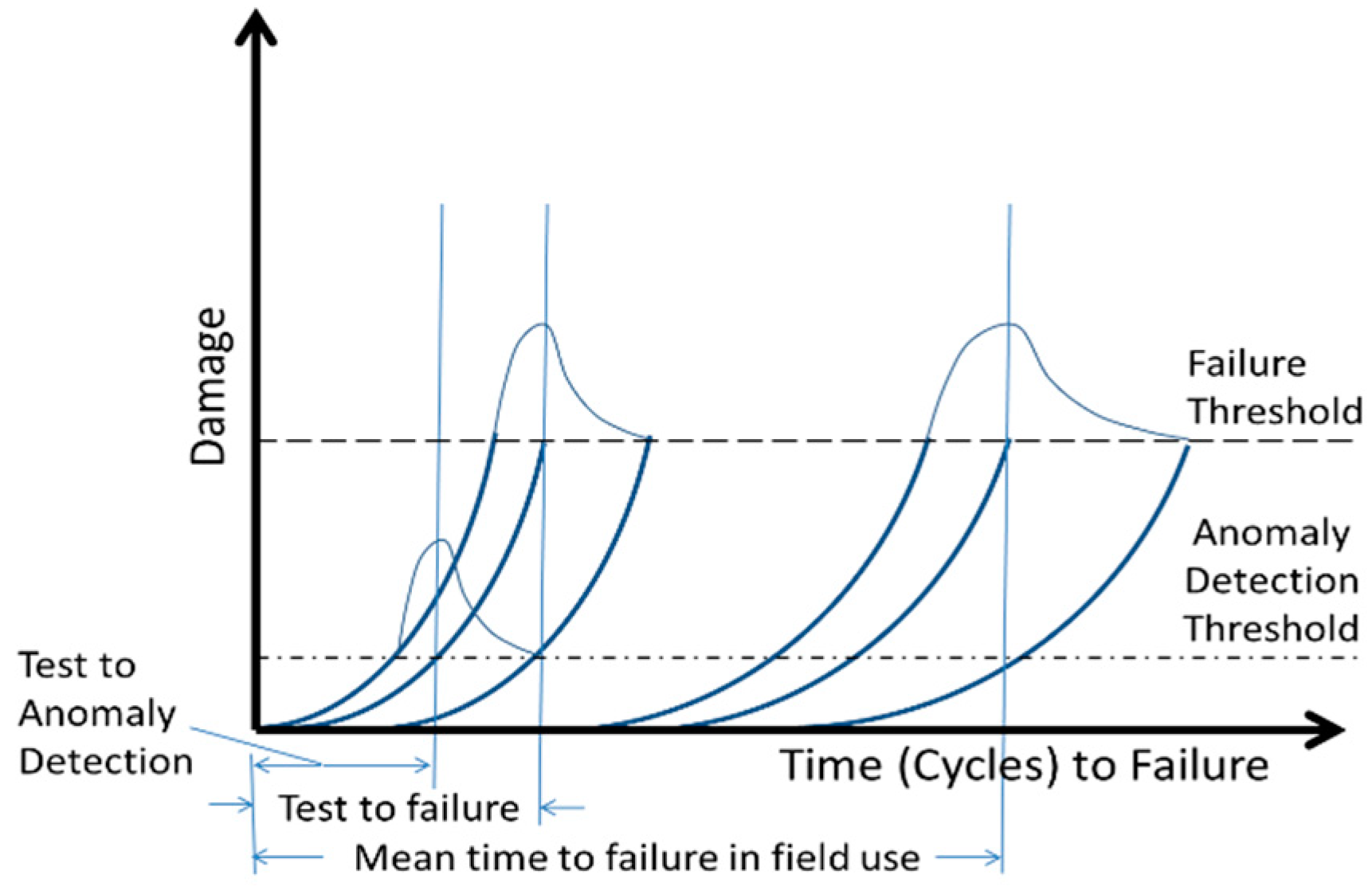
Figure 4.
The projected safe-operating area (SOA) of SiC and GaN power devices; the SOA for GaN is expected to be smaller than that of SiC due to a higher density of crystal defects in the material.
Figure 4.
The projected safe-operating area (SOA) of SiC and GaN power devices; the SOA for GaN is expected to be smaller than that of SiC due to a higher density of crystal defects in the material.
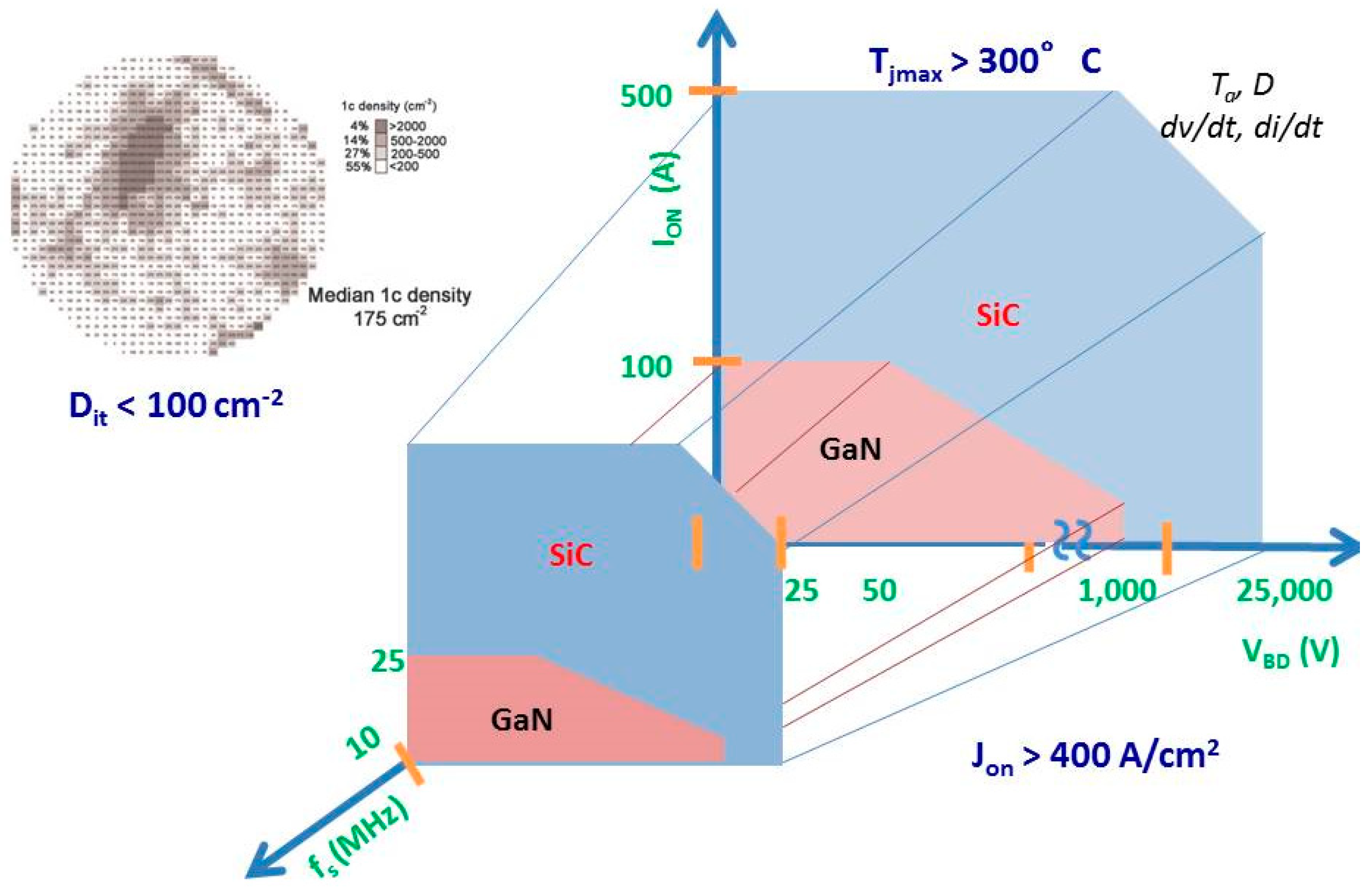
Figure 5.
Structural model of GaN threading dislocation [40].
Figure 5.
Structural model of GaN threading dislocation [40].
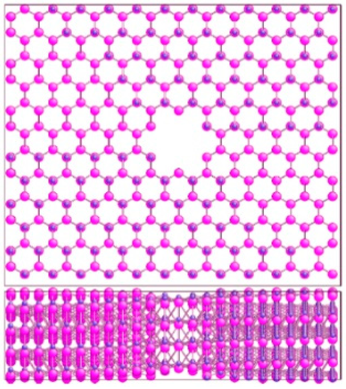
Figure 6.
The formation of threading defects in the epi-layer by the substrate steps [45]. (a) High-resolution TEM (HRTEM) characterization of defects at the interface. (b) Atomistic model of mismatch boundary resulting from interfacial steps at the substrate.
Figure 6.
The formation of threading defects in the epi-layer by the substrate steps [45]. (a) High-resolution TEM (HRTEM) characterization of defects at the interface. (b) Atomistic model of mismatch boundary resulting from interfacial steps at the substrate.

Figure 7.
Design of interfaces for reducing defects in the epilayer by increasing formation energy.
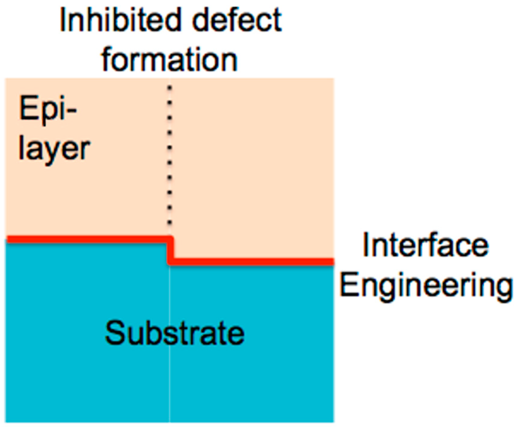
Figure 8.
X-ray topography of GaN/GaN showing a nearly uniform distribution of strain centers. The grazing incidence topography is similar to the transmission image; the grazing image also shows the nearly uniform distribution of strain centers. The X ray image shows that individual threading dislocations are not resolved showing a relatively low dislocation density in those regions. The cathodoluminescence (CL) image on the right shows a defect density of greater than 104 cm−2 [61].
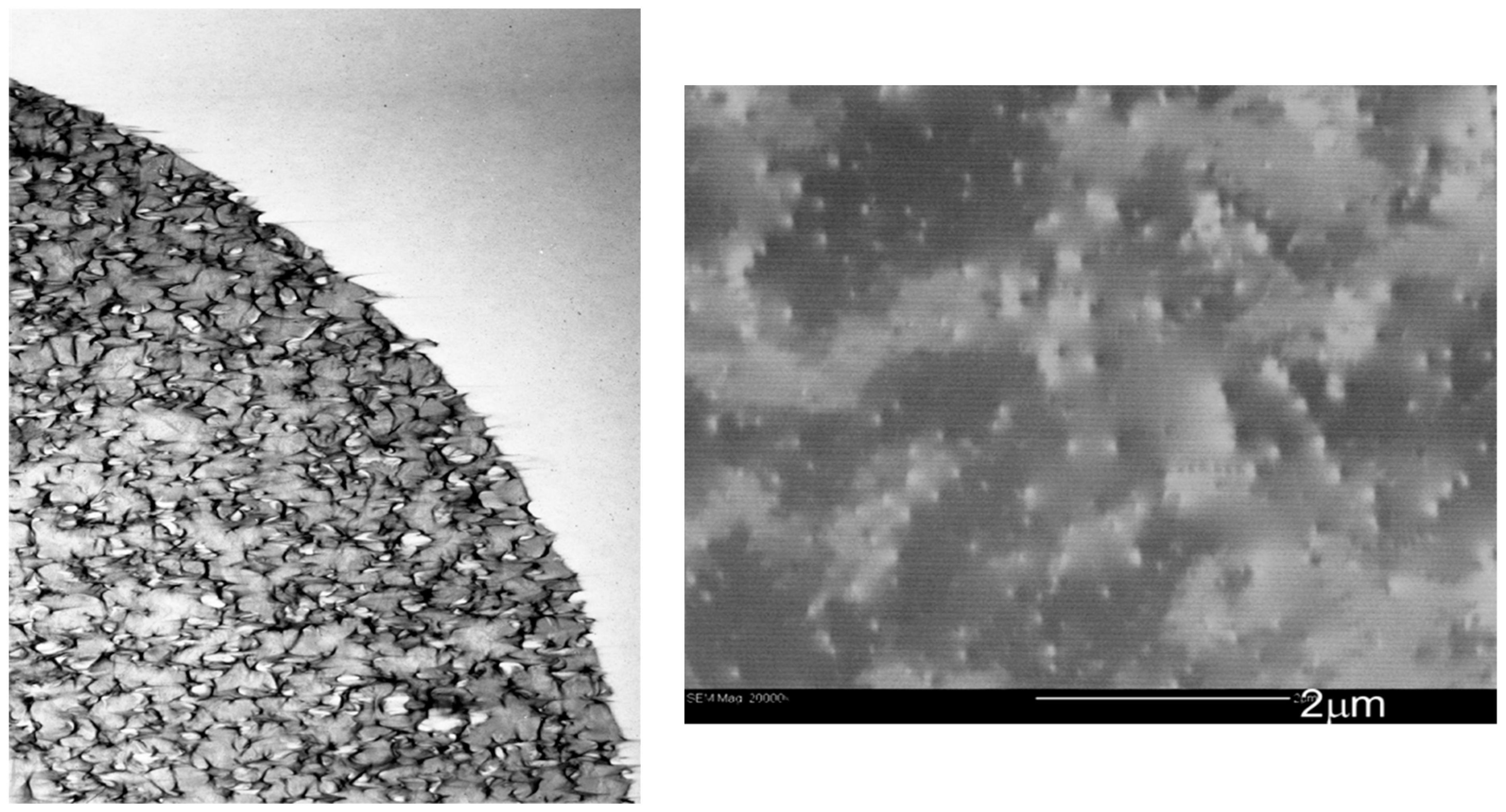
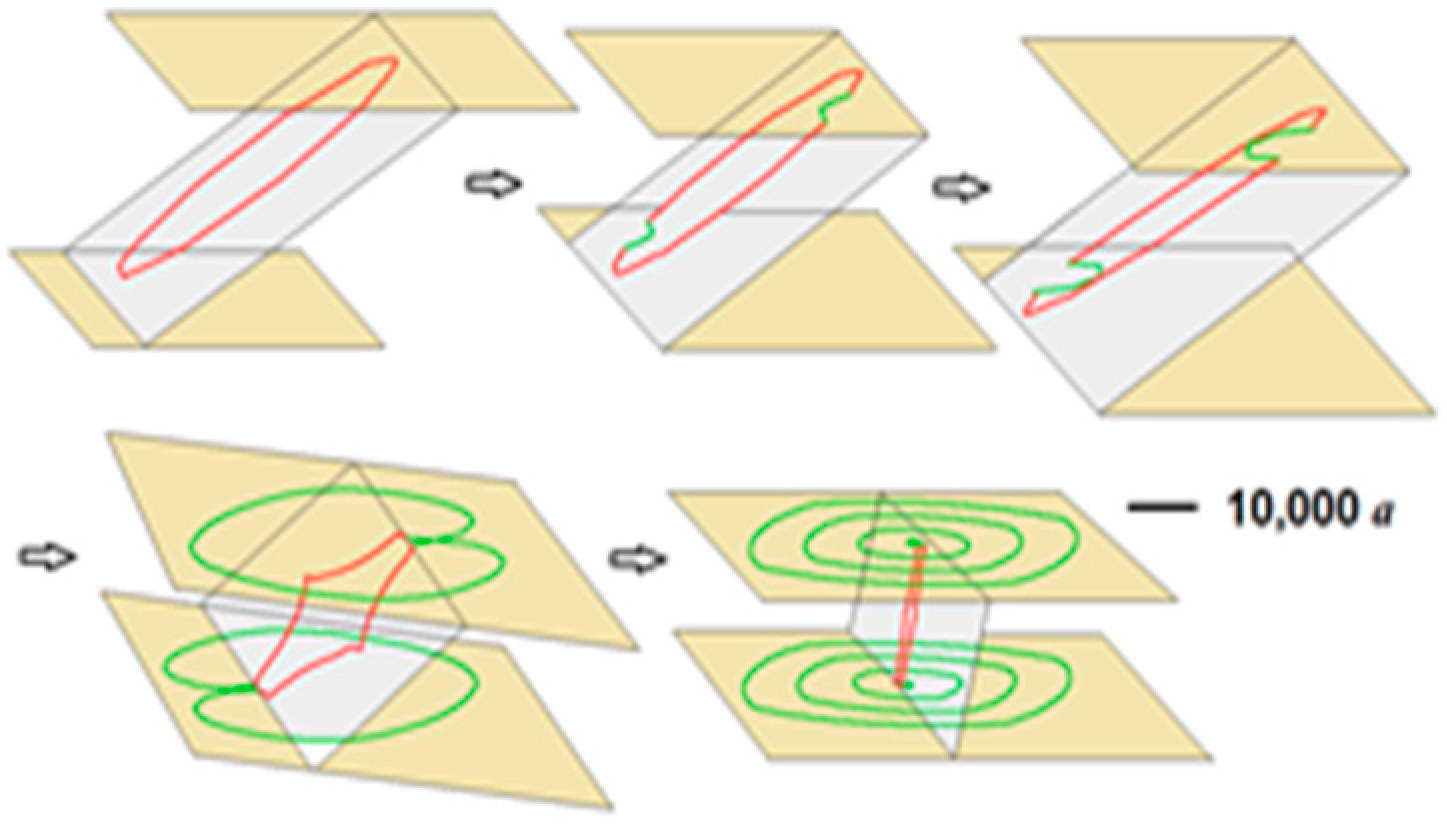
Figure 9.
Discrete dislocation dynamics simulation of cross-slip of pyramidal Shockley loops on basal planes [56].
Figure 9.
Discrete dislocation dynamics simulation of cross-slip of pyramidal Shockley loops on basal planes [56].

Table 1.
Summary of WBG device characteristics and the challenges posed by defects.
| Characteristic | Challenges |
|---|---|
| Effects of high-temperature stress on metal–semiconductor interface |
|
| Cosmic ray-induced failures |
|
| On-state static electrical stress |
|
| Off-state static electrical stress |
|
| High-voltage and high-current switching stress |
|
| Electron transport under high magnetic field stress |
|
| Impact of epitaxial defects on electron transport |
|
| Defect evolution under stresses and large temperatures |
|
Publisher’s Note: MDPI stays neutral with regard to jurisdictional claims in published maps and institutional affiliations. |
© 2021 by the authors. Licensee MDPI, Basel, Switzerland. This article is an open access article distributed under the terms and conditions of the Creative Commons Attribution (CC BY) license (https://creativecommons.org/licenses/by/4.0/).
Share and Cite
MDPI and ACS Style
Setera, B.; Christou, A. Challenges of Overcoming Defects in Wide Bandgap Semiconductor Power Electronics. Electronics 2022, 11, 10. https://doi.org/10.3390/electronics11010010
AMA Style
Setera B, Christou A. Challenges of Overcoming Defects in Wide Bandgap Semiconductor Power Electronics. Electronics. 2022; 11(1):10. https://doi.org/10.3390/electronics11010010
Chicago/Turabian StyleSetera, Brett, and Aristos Christou. 2022. "Challenges of Overcoming Defects in Wide Bandgap Semiconductor Power Electronics" Electronics 11, no. 1: 10. https://doi.org/10.3390/electronics11010010
Note that from the first issue of 2016, this journal uses article numbers instead of page numbers. See further details here.