
A Circuit-Based Wave Port Boundary Condition for the Nodal Discontinuous Galerkin Time-Domain Method

School of Electronic Engineering, Xidian University, Xi’an 710071, China
*
Author to whom correspondence should be addressed.
Electronics 2022, 11(12), 1842; https://doi.org/10.3390/electronics11121842
Submission received: 17 May 2022
/
Revised: 8 June 2022
/
Accepted: 9 June 2022
/
Published: 9 June 2022
(This article belongs to the Special Issue Recent Advancements and Applications of Computational Electromagnetics)
Abstract
:Waveguide-like transmission line (WLTL) structures, including rectangular waveguides, circular waveguides, and coaxial lines, have been widely used in microwave engineering. Determining how to efficiently model WLTLs has become vital for the design of various WLTL-based devices. In this paper, a circuit-based wave port boundary condition (CWPBC) is developed and applied in the discontinuous Galerkin time-domain (DGTD) method to accurately simulate these structures for the first time. In the CWPBC, modal voltages and currents of a WLTL are defined, and circuits based on modal voltages and currents are introduced. By co-simulating the modal circuit and the WLTL modeled using the DGTD method, various modal fields can be excited in the WLTL, and at the same time, the WLTL can be terminated without reflections. No extra costs or approximations are used in the proposed CWPBC, and there is no requirement of either the extension of the computational domains widely used in perfectly matched layer (PML) termination or the longitudinal field continuity used in the reported DGTD method. The proposed method can easily obtain the postprocessing parameters, including S-parameters and port power. Numerical results, including rectangular waveguide filters, circular waveguide horns, and coaxial-fed electromagnetic bandgaps (EBG), are given to validate the effectiveness of the proposed CWPBC.
1. Introduction
In recent years, the discontinuous Galerkin time-domain (DGTD) method, as a transient solver with high performance, has attracted much attention [1,2,3,4,5,6,7,8,9,10,11,12]. The DGTD method can be regarded as a combination of the finite element method (FEM) and the finite volume method (FVM) because it has inherited the advantages of both methods, such as a flexible modeling ability, good solution accuracy, elementwise solutions, and a natural parallelization ability. Therefore, the DGTD method has been widely used to analyze various complex electromagnetic problems, for instance, electromagnetic/circuit co-simulation [6], graphene-based devices [7], and multiscale complex electromagnetic problems [10,11].
Waveguide-like transmission lines (WLTLs), including rectangular waveguides, circular waveguides, and coaxial lines, have many important applications in microwave engineering, for instance, in filters, couplers, antennas, and feeding structures [13]. For the simulation of these structures, truncation boundary conditions without reflections need to be introduced. One of the most commonly employed techniques for truncation is the use of perfectly matched layers (PMLs) [14]. PMLs can absorb incoming waves without reflections. However, the implementation of PMLs requires an extra computational domain, thus resulting in more computational costs. In addition to PMLs, the waveguide port boundary condition (WPBC) has been widely used to accurately truncate WLTLs in terms of analytical modal expansions. Two kinds of methods for the good absorption of modal fields have been developed. One is to couple a 3D WLTL with an auxiliary 1D transmission line with the same dispersive property [15,16,17,18,19]. However, in order to avoid reflections from the termination of the 1D transmission line, a long enough 1D transmission line is required, thus resulting in extra computational burdens [19]. The other method is to express transverse modal fields using the longitudinal modal fields in FEM [20,21,22]. When the WPBC is applied in the DGTD method, longitudinal field continuity at the port is implemented [23,24]. However, it is unnecessary for the DGTD method to guarantee longitudinal field continuity, which possibly affects the performance of the conventional DGTD method.
In this paper, a reflection-free circuit-based WPBC (CWPBC) boundary condition is proposed for the first time to terminate WLTLs. A modal circuit representing the modal voltage and the modal current is introduced. The co-simulation of the modal circuit and the WLTL solved using the DGTD method is implemented. With the modal circuit, modal fields can be excited and absorbed without reflections. With the proposed CWPBC, the parameters, including S-parameters and port power, can be easily obtained. The proposed field-circuit cooperative implementation avoids not only some of the extra computations caused by the PML region in [14] and the auxiliary 1D transmission line in [19] but also the unnecessary longitudinal field continuity in [23,24]. Therefore, the proposed CWPBC method has higher computational efficiency with better computational accuracy. This paper is organized as follows: In Section 2, a brief overview of the DGTD method is given, followed by the modal circuit-based CWPBC for WLTLs in Section 3. The co-simulation of the modal circuit and the WLTL is implemented in Section 4. Three numerical examples are discussed in Section 5. Conclusions are given in Section 6.
2. The DGTD Method
A 3D computational domain Ω with permittivity ε and permeability μ is considered. A group of tetrahedrons Ωk with surfaces ∂Ωk (k = 1, …, K0) is used to discretize Ω. In each tetrahedron, the electric field Ek and the magnetic field Hk are expanded in terms of the Nth-order Lagrange scalar functions, which are defined on the Np Legendre–Gauss–Lobatto (LGL) quadrature points. Here, Np = (N + 1)(N + 2)(N + 3)/6. Specifically,
in which with the jth Lagrange polynomial , and (u = e,h) with (u = E,H; s = x,y,z). Here, denotes the value of at the ith interpolation point .
By inserting Equations (1) and (2) into two Maxwell curl equations, and by performing the Galerkin spatial testing procedure and the Gauss theorem twice with the resultant equation, one obtains the semi-discrete form as follows:
where is the outward normal unit vector across face f, and and denote the jumps of the numerical traces between the kth element and its adjacent element. Here, superscript “+” represents the neighboring element of the kth element, and Nf is the number of neighboring elements. Note that in the derivations of Equations (3) and (4), the center flux is used. The mass matrix [M]k, the stiffness matrix [S]k, and the flux matrix [F]k,f are given, respectively, as
where
With the approximation of the leap-frog scheme for the time derivative, the full-discrete form can be given as
where superscript “n” is the nth time.
3. The Modal Circuit-Based WPBC
In a uniform WLTL, whose cross-section is of arbitrary shape and remains unchanged along the longitudinal direction, e.g., z., as shown in Figure 1, electromagnetic fields can be decomposed into the transverse magnetic (TM) mode and the transverse electric (TE) mode along the transmission direction. The TE and TM longitudinal modal functions can be obtained according to the 2D Helmholtz equation with different boundary conditions, respectively, as [25]
where represents the transverse Nabla operator, denotes the cutoff frequency, and S is the cross-section of the waveguide with the contour . With solved, the transverse modal fields can be solved as
and
For convenience, the transverse modal fields of () and () are sorted in ascending order according to their cutoff frequencies, and the superscripts “TE” and “TM” are omitted. Note that the transverse modal fields are orthonormal, i.e.,
Moreover, the relationship between the transverse modal electric fields and the transverse modal magnetic fields is
Therefore, the transverse components of the frequency-domain fields in the WLTL can be expressed in terms of the transverse modal fields as
in which the expansion coefficients of the transverse components of the electromagnetic fields and are solved as
By inserting Equation (15) into the following transverse Maxwell’s equations in the WLTL [25]
and by applying the testing procedure in Equation (17) using transverse modal fields and , respectively, one obtains
where the constants A1 and A2 related to the modes are
Note that in deriving Equation (18), the condition that the transverse components of the electromagnetic fields satisfy the 2D Helmholtz equation is applied, i.e.,
.
Furthermore, (18) is rewritten as
in which is the mode propagation constant, and is the mode characteristic impedance with the following expression:
It can be seen from Equation (21) that and the satisfy the telegraph’s equation governing the voltage and the current on the transmission line, and, thus, and are called the modal voltage and modal current, respectively.
The solution of Equation (21) can be expressed as the superposition of the incident and reflection modal voltages/currents. At z = z0, the relationship between and can be obtained as
where is the modal current source, and is the incident modal current. According to Equation (23), the equivalent modal circuit describing the modal voltage and the modal current can be given, as seen in Figure 2. At the port of z = z0, the ith modal field in the WLTL is excited by the modal circuit with the modal current source .
When transforming Equation (23) into the time domain, one obtains
in which Ii(t) and Vi(t) are counterparts in the time domain of and , respectively; “*” represents the convolution operation; and the characteristic admittance Yi is
and
where , J1 is the 1st-order Bessel function of the first kind, denotes the Dirac function, and c is the speed of light.
By inserting Equation (25) or (26) into (24) and by performing the time discretization, one obtains
where denotes the convolution term in Equation (24) at the nth time.
When the modal circuit shown in Figure 2 is implemented at the port of z = z0, the ith mode field in the waveguide can be well excited. However, when the modal circuit without the modal current source, i.e., the load Yi, is connected to the waveguide, the ith mode field can be absorbed without reflections. The resulting truncation boundary condition for the WLTL is called the CWPBC.
4. Co-Simulation of Modal Circuit and WLTL
4.1. Field-Circuit Co-Simulation
In order to implement the CWPBC, the co-simulation of the modal circuit and waveguide is introduced, as shown in Figure 3.
It is considered that the port plane is located at z = z0 and that the WLTL is placed in the region of z > z0. The modal equivalent circuit is connected to the WLTL at z = z0. In order to truncate the computational domain at z = z0 to reduce unnecessary computation, a truncation boundary condition is placed. The common boundary conditions in the DGTD method include a perfect magnetic conductor (PMC), a perfect electric conductor (PEC), and a first-order absorbing boundary condition (ABC). For the PMC, the jumps of the numerical traces are only related to the magnetic fields. For the PEC, the jumps are only related to the electric fields. By comparison, the jumps of the numerical traces of the ABC simultaneously involve the electric fields and the magnetic fields. Therefore, the computational costs of the PMC and the PEC are less than those of the ABC. Considering that the modal equivalent circuit is based on the modal current source given by Equation (23), the PMC boundary is used. This is because the radiations cannot be generated by the electric currents placed on the surface of the PEC. Note that the modal equivalent circuit can be also given in terms of the modal voltage source by the dual transformation of Equation (23), and, accordingly, the PEC is employed for the truncation.
When the PMC boundary is used at z = z0, the corresponding jumps of the numerical traces become
It is worth pointing out that the jumps of the magnetic fields in (28) are obtained according to Huygens’ principle, which are twice as much as those widely used in the DGTD method.
Due to the zero jumps of the electric fields in Equation (28), (8) can be explicitly solved for . However, Equation (7) is solved using the field-circuit co-simulation. In this scenario, the term in Equation (28) is expressed in terms of the modal currents as
in which Nm is the total number of modes absorbed by the CWPBC. When using the central approximation, at the (n + 1/2) th time is obtained as
By inserting Equations (28) and (30) into (7), one obtains
where
However, according to the first equation in (16), we have
where Ne denotes the number of elements at the port plane, and
By combining Equations (27), (31), and (33), the coupled matrix equation for the CWPBC can be obtained as
in which
By explicitly solving Equation (35), , , and can be obtained. Note that without the modal voltage and current, (35) is reduced to the governing equation of the electric field in the conventional DGTD method, i.e., (7). It is worth pointing out that the stability condition of the DGTD method with the CWPBC can be theoretically derived according to the matrix decomposition-based eigenvalue solution method [11]. We also find through the vast numerical examples that the time step is not reduced with the use of the CWPBC.
4.2. S-Parameters and Port Power
Once the electromagnetic fields, the modal voltages, and the modal currents are obtained, the postprocessing parameters, including S-parameters and port power, can be easily obtained. The scattering parameter S (m:i, n:j) between the ith mode reflecting wave at port m, i.e., , and the jth mode incident excitation at port n, i.e., , is calculated using
in which
However, the computation of the port power can be simply obtained according to the canonical orthogonality properties of the modal fields. For port n with M modes, the input power is solved as
By inserting Equation (15) into (40), one obtains
5. Results and Discussion
In this section, three numerical examples are given to show the validity and the effectiveness of the proposed CWPBC. The port of the WLTL is assumed to be a closed homogenous port with an arbitrary cross-section.
5.1. Performance Validation
In the first example, a WR90 rectangular waveguide with a size of 22.86 mm × 10.16 mm × 40 mm is considered to validate the performance of the proposed CWPBC, as shown in Figure 4a. The waveguide is discretized by elements with an average size of 1/6 λ10GHz, and, thus, the number of elements is 448. The time step of 4.59 × 10⁻¹³ s is used. For comparison, an unsplit PML with a thickness of 8/10 λ10GHz is also used to terminate the two ends of the waveguide. In the PML region, the average size of the discretization element is 1/10 λ10GHz, and in the waveguide, the average size of the discretization element is 1/6 λ10GHz, thus resulting in 3621 elements. The time step is chosen as 1.67 × 10⁻¹³ s. The transient mode current source Is = 2Iinc is enforced to excite the TE10 mode, and the waveform of the incident mode current Iinc is shown in Figure 4b. The transient waveforms of the excited mode currents at ports 1 and 2 are plotted in Figure 4b. It can be seen that the waveform of the mode current at port 1 coincides with that of the incident mode current, and the waveform of the mode current at port 2 is the same as that at port 1, with a time delay caused by wave propagation in the waveguide.
A performance comparison between the proposed CWPBC and the PML is presented in Figure 4c. The S11 of the proposed CWPBC is better than that of the PML. Note that, compared with the proposed CWPBC, more elements and unknowns are required due to the introduction of the PML region. In addition, the frequency-domain FEM with the wave port method is adopted, and the corresponding results are shown in Figure 4c. In the lower band, the FEM result is better than the result obtained using the proposed CWPBC, while in the higher band, the FEM result is worse than the result obtained using the proposed CWPBC.
Furthermore, a comparison of CPU time consumption among the PML, the WPBC, and the proposed CWPBC is presented in Table 1. Here, 1000 time steps are performed to calculate the CPU time. In Table 1, it can be seen that the proposed CWPBC method consumes less computational time than the PML and the WPCB. The ratio of the computational time consumed by the proposed CWPBC method to that of the PML is 0.073.
5.2. Waveguide Filter
In the second example, a seventh-order rectangular waveguide filter is provided to demonstrate the accuracy of the proposed CWPBC. The geometry of the filter is shown in Figure 5a. Two rectangular ports with a size of 28.5 mm × 12.63 mm, called port 1 and port 2, are used to truncate the computational region. Since the filter only operates in the dominant mode, i.e., the TE10 mode, the modal circuit related to the dominant mode is used in this example. The ports are discretized by tetrahedrons with an average edge length of 1/20 λ7.5GHz, the iris and slot parts are discretized by tetrahedrons with an average edge length of 1/40 λ7.5GHz, and the remaining part is discretized by tetrahedrons with an average edge length of 1/10 λ7.5GHz, thus resulting in 76,800 elements. The second-order basis functions are used to expand the unknown electric and magnetic fields. The time step ∆t = 6.9 × 10⁻¹⁴ s is employed for the stable solution. The S-parameters, including S11 and S21, are solved using the proposed method, and they are compared with those of the FEM results, as shown in Figure 5b,c. A good agreement between them is observed.
5.3. Circular Horn Antenna
In this section, a dual-mode circular horn antenna is considered. Figure 6a gives the dimensions of the horn antenna. When the dominant mode of the horn, i.e., the TE11 mode, is excited, the TE11 mode can be converted to the TM11 mode, and two modes can be radiated at the same time. In this example, the modal circuit related to the first 10 modes is used. The whole computational domain with a size of 0.26 m × 0.26 m × 0.49 m is terminated by the first-order ABC boundary condition. The region close to the horn is discretized by elements with an average size of the 1/10 λ10GHz, and the remaining region is discretized by elements of an average size of 1/4 λ10GHz. At the port, an element with an average size of 1/20 λ10GHz is used. A total of 617571 elements with second-order basis functions are implemented, and the time step ∆t = 1.0 × 10⁻¹⁴ s is chosen. Figure 6b presents the S11 curves of the TE11 mode and the TM11 mode solved using the proposed method and the FEM, and they are in good agreement with each other. Figure 6c presents a comparison of directivity at 10 GHz in the xoz plane between the proposed method and the FEM. A good agreement between the two results is observed
5.4. Electromagnetic Bandgap (EBG) Structure
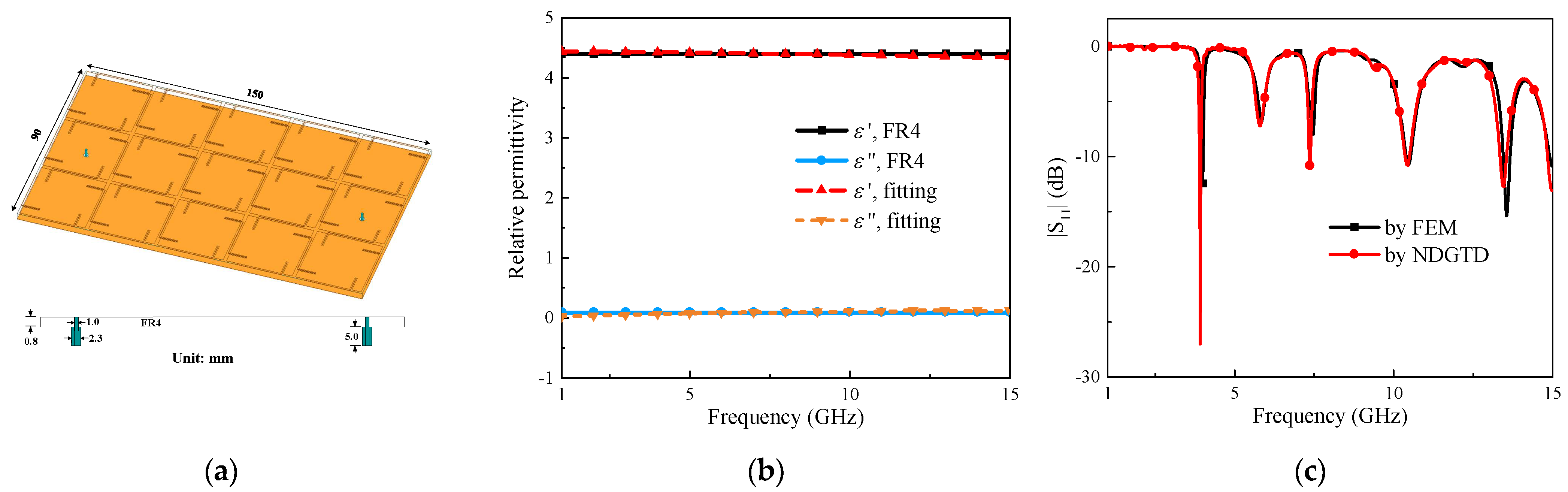
Finally, a uniplanar compact EBG structure with L-bridges and slits (LBS-EBG) is considered for the application of the ground bounce noise (GBN), as shown in Figure 7a. The EBG with 3 × 5 unit cells is fabricated on an FR4 substrate with a relative permittivity of 4.4 and a loss tangent of 0.02. Two coaxial probes with the characteristic impedance of 50 Ω are inserted in the LBS-EBG. The dominant mode, i.e., transverse electromagnetic (TEM) mode, is excited by the coaxial port. The detailed dimensions of the unit cell can be found in [26].
In the DGTD method, a vector-fitting technique is used to approximate the relative permittivity of the substrate in the band of 1~15 GHz as a partial fraction in terms of real and/or complex-conjugate pole–residue pairs [7], as shown in Figure 7b. The discretization mesh sizes at the port and near the port are 1/75 λ10GHz and 1/60 λ10GHz, respectively, and the mesh size of the remaining region is set as 1/30 λ10GHz. A total of 673254 tetrahedrons are generated, and second-order basis functions are used. The time step ∆t = 3.5 × −15 s is chosen. S11 is solved using the proposed method and the FEM. A good agreement is obtained, as shown in Figure 7c.
6. Conclusions
This paper develops a circuit-based wave port boundary condition for the nodal discontinuous Galerkin time-domain method. A modal-equivalent circuit in terms of the modal voltage and the modal current is proposed, and a co-simulation between the field and the circuit is implemented to achieve the excitation of the modal fields and the truncation of the waveguide-like transmission line without reflections. Numerical examples, including the rectangular waveguide, the circular waveguide, and the coaxial port, are given to demonstrate the feasibility of proposed method in the solution of practical electromagnetic problems.
It is worth pointing out that the proposed circuit-based wave port boundary condition can accurately truncate waveguide-like transmission lines with frequency-invariant modal fields. The extension of the proposed method to transmission lines with dispersive modal fields is our future research direction.
Author Contributions
Conceptualization, S.Z. and Y.S.; methodology, S.Z.; software, S.Z. and Z.B.; formal analysis, S.Z., Y.S. and Z.B.; investigation, S.Z.; data curation, S.Z.; writing—original draft preparation, S.Z.; writing—review and editing, Y.S.; visualization, S.Z. and Y.S.; supervision, Y.S.; funding acquisition, Y.S. All authors have read and agreed to the published version of the manuscript.
Funding
This research was funded by the National Key Research and Development Program of China (No. 2021YFA1401001).
Data Availability Statement
The data presented in this study are available on request from the corresponding author.
Conflicts of Interest
The authors declare no conflict of interest.
References
- Hesthaven, J.S.; Warburton, T. Nodal Discontinuous Galerkin Methods: Algorithms, Analysis, and Applications; Springer: New York, NY, USA, 2008. [Google Scholar]
- Angulo, L.D.; Alvarez, J.; Pantoja, M.F.; Garcia, S.G.; Bretones, A.R. Discontinuous Galerkin time domain methods in computational electrodynamics: State of the art. Forum Electromagn. Res. Methods Appl. Technol. 2015, 10, 1–24. [Google Scholar]
- Li, X.L.; Jin, J.M. A comparative study of three finite element-based explicit numerical schemes for solving Maxwell’s equations. IEEE Trans. Antennas Propag. 2012, 60, 1450–1457. [Google Scholar] [CrossRef]
- Chen, J.F.; Liu, Q.H. Discontinuous Galerkin time-domain methods for multiscale electromagnetic simulations: A review. Proc. IEEE 2013, 101, 242–254. [Google Scholar] [CrossRef]
- Dosopoulos, S.; Lee, J.F. Interior penalty discontinuous Galerkin finite element method for the time-dependent first order Maxwell’s equations. IEEE Trans. Antennas Propag. 2010, 58, 4085–4090. [Google Scholar] [CrossRef]
- Tian, C.Y.; Shi, Y.; Shum, K.M.; Chan, C.H. Wave equation-based discontinuous Galerkin time domain method for co-simulation of electromagnetics-circuit systems. IEEE Trans. Antennas Propag. 2020, 68, 3026–3036. [Google Scholar] [CrossRef]
- Wang, P.; Shi, Y.; Tian, C.Y.; Li, L. Analysis of Graphene-based devices using wave equation-based discontinuous Galerkin time domain method. IEEE Antennas Wirel. Propag. Lett. 2018, 17, 2169–2173. [Google Scholar] [CrossRef]
- Tian, C.Y.; Shi, Y.; Chan, C.H. An improved vector wave equation-based discontinuous Galerkin time domain method and its hybridization with Maxwell’s equation-based discontinuous Galerkin time domain method. IEEE Trans. Antennas Propag. 2018, 66, 6170–6178. [Google Scholar] [CrossRef]
- Shi, Y.; Tian, C.Y.; Liang, C.H. Discontinuous Galerkin time-domain method based on marching-on-in-degree scheme. IEEE Antennas Wirel. Propag. Lett. 2017, 16, 250–253. [Google Scholar] [CrossRef]
- Ban, Z.G.; Shi, Y.; Yang, Q.; Wang, P.; Zhu, S.C.; Li, L. GPU-accelerated hybrid discontinuous Galerkin time domain algorithm with universal matrices and local time stepping method. IEEE Trans. Antennas Propag. 2020, 68, 4738–4752. [Google Scholar] [CrossRef]
- Ban, Z.G.; Shi, Y.; Wang, P. Advanced parallelism of DGTD method with local time stepping based on novel MPI + MPI unified parallel algorithm. IEEE Trans. Antennas Propag. 2022, 70, 3916–3921. [Google Scholar] [CrossRef]
- Li, P.; Jiang, L.J.; Bagci, H. Transient analysis of dispersive power-ground plate pairs with arbitrarily shaped antipads by the DGTD method with wave port excitation. IEEE Trans. Electromag. Compat. 2017, 59, 172–183. [Google Scholar] [CrossRef]
- Bansal, M.; Singh, H.; Sharma, G. A taxonomical review of multiplexer designs for electronic circuits & devices. J. Electron. Inform. 2021, 3, 77–88. [Google Scholar]
- Berenger, J.P. A perfectly matched layer for the absorption of electromagnetic waves. J. Comput. Phys. 1994, 114, 185–200. [Google Scholar] [CrossRef]
- Wolter, H.; Dohlus, M.; Weiland, T. Broadband calculation of scattering parameters in the time domain. IEEE Trans. Magn. 1994, 30, 3164–3167. [Google Scholar] [CrossRef]
- Geib, B.; Dohlus, M.; Weiland, T. Calculation of scattering parameters by orthogonal expansion and finite integration method. Int. J. Numer. Model. 1994, 7, 377–398. [Google Scholar] [CrossRef]
- Alimenti, F.; Mezzanotte, P.; Roselli, L.; Sorrentino, R. Modal absorption in the FDTD method: A critical review. Int. J. Numer. Model. 1997, 10, 245–264. [Google Scholar] [CrossRef]
- Chen, G.; Stang, J.; Moghaddam, M. A conformal FDTD method with accurate waveport excitation and S-parameter extraction. IEEE Trans. Antennas Propag. 2016, 64, 4504–4509. [Google Scholar] [CrossRef]
- Potratz, C.; Glock, H.; Rienenk, U.V. Time-domain field and scattering parameter computation in waveguide structures by GPU-accelerated discontinuous-Galerkin method. IEEE Trans. Microw. Theory Technol. 2011, 59, 2788–2797. [Google Scholar] [CrossRef]
- Lou, Z.; Jin, J.M. An accurate waveguide port boundary condition for the time-domain finite-element method. IEEE Trans. Microw. Theory Technol. 2005, 53, 3014–3023. [Google Scholar]
- Wang, R.; Jin, J.M. A symmetric electromagnetic-circuit simulator based on the extended time-domain finite element method. IEEE Trans. Microw. Theory Technol. 2008, 56, 2875–2884. [Google Scholar] [CrossRef]
- Loh, T.H.; Mias, C. Implementation of an exact modal absorbing boundary termination condition for the application of the finite-element time-domain technique to discontinuity problems in closed homogeneous waveguides. IEEE Trans. Microw. Theory Technol. 2004, 52, 882–888. [Google Scholar] [CrossRef]
- Zhao, L.; Chen, G.; Yu, W.; Jin, J.M. A fast waveguide port parameter extraction technique for the DGTD method. IEEE Antennas Wirel. Propag. Lett. 2017, 16, 2659–2662. [Google Scholar] [CrossRef]
- Chang, C.P.; Chen, G.; Yan, S.; Jin, J.M. Waveport modeling for the DGTD simulation of electromagnetic devices. Int. J. Numer. Model. 2018, 31, e2226. [Google Scholar] [CrossRef]
- Marcuvitz, N. Waveguide Handbook; IET: London, UK, 1986. [Google Scholar]
- Li, L.; Chen, Q.; Yuan, Q.; Sawaya, K. Ultrawideband suppression of ground bounce noise in multilayer PCB using locally embedded planar electromagnetic band-gap structures. IEEE Antennas Wirel. Propag. Lett. 2009, 8, 740–743. [Google Scholar]
Figure 1.
A uniform WLTL: (a) cross-section view and (b) longitudinal view.

Figure 2.
Equivalent modal excitation circuit for the WLTL.
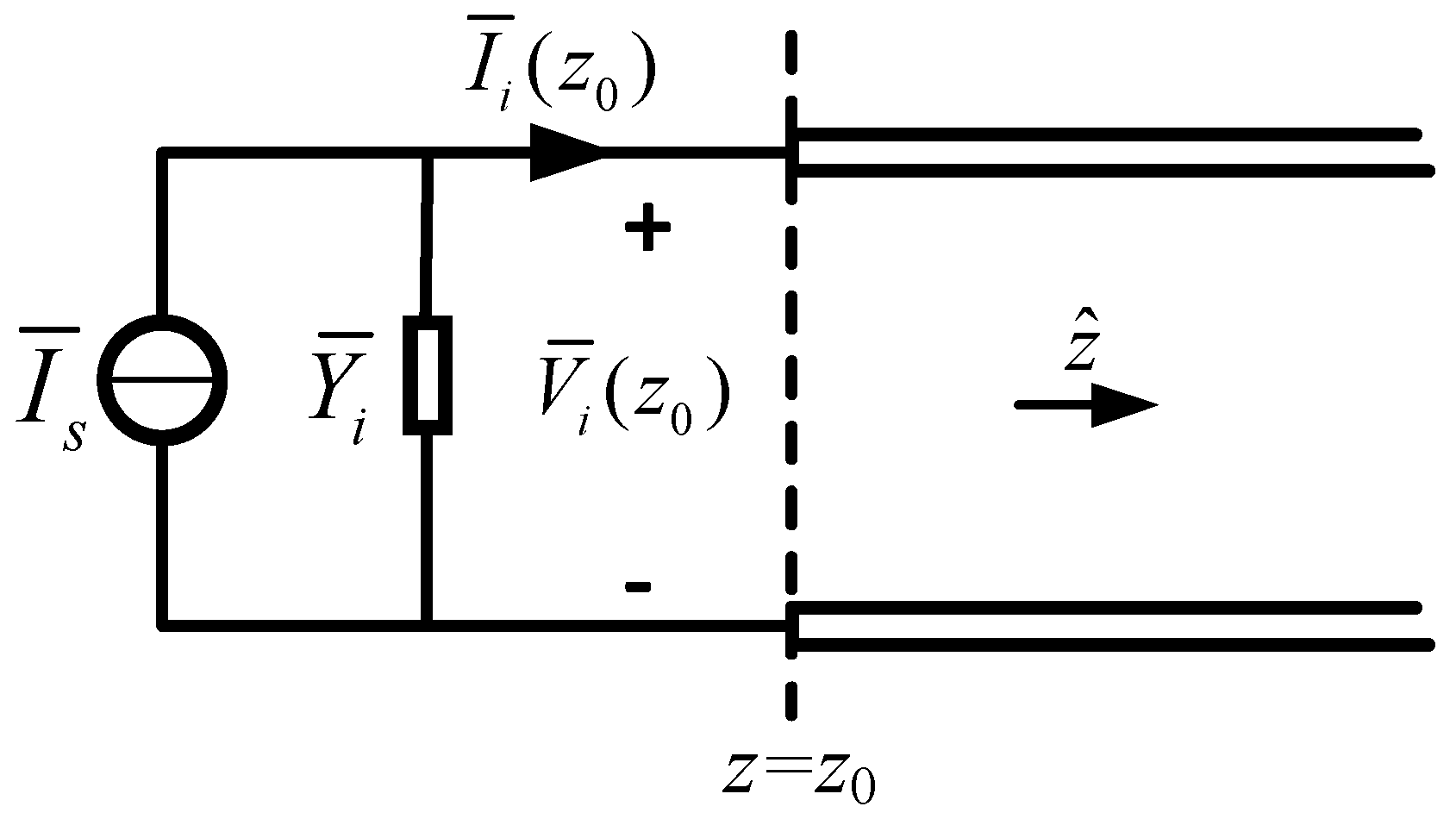
Figure 3.
Equivalent modal excitation circuit for the WLTL.

Figure 4.
Performance comparison between the CWPBC and the PML: (a) topology, (b) mode current, and (c) S-parameters.
Figure 4.
Performance comparison between the CWPBC and the PML: (a) topology, (b) mode current, and (c) S-parameters.

Figure 5.
A 7th-order rectangular waveguide filter: (a) topology, (b) S11, and (c) S21. Dimensions of the wave port are b = 28.5 mm and a = 12.63 mm. The corner radius of cavities is r = 2 mm, and the other cavity sizes are l1 = 20.35 mm, l2 = 24.03 mm, l3 = 24.58 mm, l4 = 24.2 mm, l5 = 20.2 mm, l6 = 22.12 mm, l7 = 21.8 mm, w1 = w5 = 27 mm, w2 = w3 = w4 = 28 mm, w6 = 35.5 mm, and w7 = 36.5 mm. The sizes of the slots are a1 = 3 mm, b1 = 132 mm, c1 = 2 mm, a2 = 3 mm, b2 = 10 mm, and c2 = 4.82 mm.

Figure 6.
Dual-mode circular horn antenna: (a) topology, (b) S-parameters, and (c) directivity at 10 GHz. The contour of the horn is a polygon formed by connecting the following points in turn: o (0, 0, 0), p1 (35.5 mm, 0, 0), p2 (35.5 mm, 0, 90 mm), p3 (38 mm, 0, 226 mm), p4 (78 mm, 0, 366 mm), p5 (101 mm, 0, 423 mm), and p6 (0, 0, 423 mm).
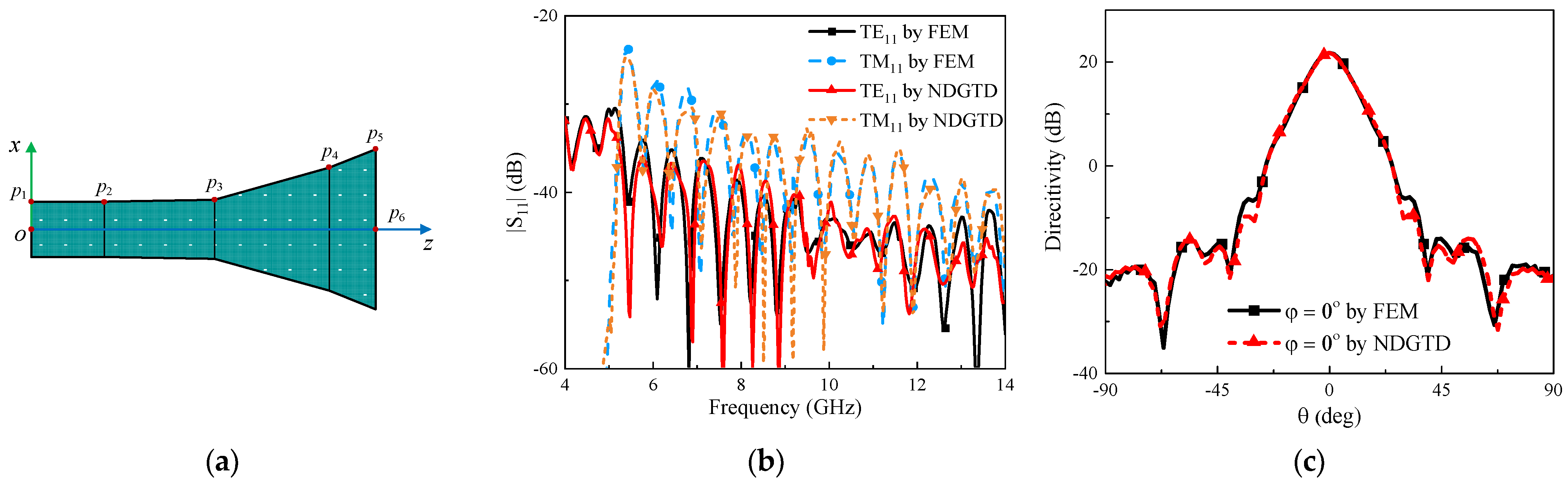
Figure 7.
LBS-EBG power plane: (a) topology, (b) relative permittivity, and (c) S-parameters.

Table 1.
Comparison of CPU time consumption among PML, WPBC, and the proposed CWPBC.
| PML | WPBC | CWPBC | |
|---|---|---|---|
| CPU time Time Ratio | 134.76 s 1 | 10.51 s 0.078 | 9.84 s 0.073 |
Publisher’s Note: MDPI stays neutral with regard to jurisdictional claims in published maps and institutional affiliations. |
© 2022 by the authors. Licensee MDPI, Basel, Switzerland. This article is an open access article distributed under the terms and conditions of the Creative Commons Attribution (CC BY) license (https://creativecommons.org/licenses/by/4.0/).
Share and Cite
MDPI and ACS Style
Zhu, S.; Shi, Y.; Ban, Z. A Circuit-Based Wave Port Boundary Condition for the Nodal Discontinuous Galerkin Time-Domain Method. Electronics 2022, 11, 1842. https://doi.org/10.3390/electronics11121842
AMA Style
Zhu S, Shi Y, Ban Z. A Circuit-Based Wave Port Boundary Condition for the Nodal Discontinuous Galerkin Time-Domain Method. Electronics. 2022; 11(12):1842. https://doi.org/10.3390/electronics11121842
Chicago/Turabian StyleZhu, Shichen, Yan Shi, and Zhenguo Ban. 2022. "A Circuit-Based Wave Port Boundary Condition for the Nodal Discontinuous Galerkin Time-Domain Method" Electronics 11, no. 12: 1842. https://doi.org/10.3390/electronics11121842
Note that from the first issue of 2016, this journal uses article numbers instead of page numbers. See further details here.