
Design for the Package-Board Transition and Its Testability Design in the Fan-Out Wafer-Level Package


1
Institute of Microelectronics, Chinese Academy of Sciences, Beijing 100029, China
2
University of Chinese Academy of Sciences, Beijing 100029, China
*
Authors to whom correspondence should be addressed.
Electronics 2022, 11(12), 1922; https://doi.org/10.3390/electronics11121922
Submission received: 7 April 2022
/
Revised: 9 June 2022
/
Accepted: 17 June 2022
/
Published: 20 June 2022
(This article belongs to the Section Microwave and Wireless Communications)
Abstract
:A fan-out wafer level package (FOWLP) with double-sided four redistribution layers (RDLs) and the mega pillars connecting the front and back RDLs has been proposed for millimeter-wave applications. A well-matched package-board transition has been designed in this paper. The simulated insertion loss for the transition is about 0.82 dB at 79 GHz, and the simulated return loss is better than 10 dB from 72 GHz to 86 GHz. More importantly, two different measurement methods based on the port reduction technique and the Thru-Reflect-Line (TRL) calibration technique have been proposed to get the S parameters of the transition. Moreover, the feasibility of the two methods has been verified by simulation.
1. Introduction
Since being introduced by Infineon in 2001 [1], because of the advantages of better thermal and electrical performance, lower cost, and good feasibility, fan-out wafer-level package (FOWLP) technology has been widely used in millimeter-wave applications [2,3,4,5,6,7,8]. Thanks to the researchers, various types of FOWLP have emerged: Freescale proposed the redistributed chip package in 2007 [9], IME extended the technology to multi-die packaging in 2008 [10] and demonstrated the reliability of 3D FOWLP [11], a package-on-package concept with the FOWLP was proposed by STATS ChipPAC in 2012 [12], TSMC also developed their InFo wafer-level packaging [13,14] at basic of the FOWLP, and in 2014, the Infineon applied the through encapsulant via (TEV) in embedded wafer level ball grid array (eWLB) for vertical interconnection [15]. In addition, heterogeneous integration of four chips and four capacitors by the FOWLP method has been demonstrated [16].
FOWLP has attracted the interest of many scholars: extensive researches on warpage prediction [17,18,19,20], thermal performance [21,22] and electrical performance [23,24,25,26] have been carried out. Electrical performance is significant for millimeter-wave applications, such as the 77 GHz automotive radar and wireless communication systems. As the frequency increases, how to achieve the low loss radio frequency (RF) transition becomes a major challenge. For the Long Range Radar (LRR), due to the high gain requirement, the antennas are generally series fed rectangular microstrip patch arrays on the printed circuit board (PCB). According to the radar equation, the automotive radar will have a larger detection range if the antennas get more input power. Smaller interconnection losses mean more input power to the antennas. Therefore, a well-matched chip-package-board transition is needed for the LRR. It is the same for wireless communication systems [4]. In addition, it is not easy to test the antennas directly in FOWLP. The FOWLP samples are usually soldered on the PCB for the evaluation and characterization of the antennas [27]. For more accurate performance evaluation, the package-board transition should be de-embedded. Thus, it is important to get the S parameters of the package-board transition in FOWLP.
Currently, the transition for chip-package-board or package-board in FOWLP have been studied by many researchers, like in [4,5,24,25,26]. In [4], a channel from microstrip on the chip to microstrip on PCB was simulated, and the simulated loss is about 2 dB from 56 GHz to 70 GHz. In [5], at 77 GHz, a chip-package-board RF transition with the insertion loss of about 1 dB and return loss of about 20 dB was achieved in the eWLB package for the automotive radar transceiver. However, the measurement technique and results for the transition in FOWLP have been rarely reported. In [23], using the output power measured by the package and on-wafer, the insertion loss of the transition has been calculated. However, the specific transmission parameters have not been solved. It is a huge challenge to measure the package-board transition in FOWLP directly because the probe cannot be placed at the test ports on the test board and redistribution layers (RDL) at the same time.
Although few studies have reported the FOWLP transition measurement technique, many similar studies can be used for reference. [28] proposed a novel concept based on the Thru-Reflect-Line (TRL) calibration algorithm for the characterization of a single transition through the wafer. [29] demonstrated the feasibility of characterizing the singled–ended electronic packages using experimental S-parameters up to 30 GHz. TRL calibration and transmission line theory techniques were used here.
This study designed a good package-board transition in the FOWLP for the 77 GHz automotive radars. Within 76–81 GHz passband, the simulated insertion loss is less than 0.91 dB, and the return loss is better than 16 dB. More importantly, two different measurement methods based on the port reduction technique [30,31] and the TRL calibration technique [32,33] have been proposed to get the S parameters of the transition. Furthermore, we verified the feasibility of these two methods by simulation.
2. Structure and Process of the FOWLP
As shown in Figure 1, the FOWLP includes the four RDLs (M1, M2, M3, M4), four dielectric layers (PI1, PI2, PI3, PI4) ( = 3.08, tan = 0.02), epoxy molding compound (EMC) ( = 3.7, tan = 0.009, h = 200 m), mega pillars, silicon chip, and solder ball arrays. The mega pillars are developed for vertical interconnection. The RDLs have a minimum line width and line spacing of 10 m. The pitch of the solder balls is 450 m, and the diameter is 250 m.
The FOWLP used in this study follows the RDL-First process, as shown in Figure 2. Firstly, spin coating a laser release layer on the glass wafer. Then, front side RDLs and the dielectric layers are fabricated on the release layer. After that, the mega pillars are made as the through-mold vias to achieve the vertical interconnection. Next, the thermal compression bonding of the chip should be accomplished. That step is followed by molding the whole reconstituted wafer using the thermal compression method. Next comes the back grinding process to get the designed thickness of the EMC. And then, the back side dielectric layer and RDL are formed. The next step is debonding the carrier wafer and attaching the solder balls. Finally, the reconstituted wafer is diced into individual packages.
3. Package-Board Transition in FOWLP
3.1. Selection of the Test Board
Ground–signal–ground (GSG) probes with 100 m or 150 m pitch should be used here to measure the S parameters of the transition up to 86 GHz. However, the minimum line width and space of standard PCB are 100 m, and then the probes can not be appropriately placed. In [23], a 50 ceramic-based coplanar waveguide (CPW) transmission line has been wire-bonded to the grounded coplanar waveguide (GCPW) on the PCB to complete the probe-based testing. However, extra de-embedding structures must be used to remove the influences of the GCPW-Bond wire-Ceramic CPW transition. Therefore, to avoid extra de-embedding work, we use the ceramic substrate instead of the PCB and then the probe can touch the GCPW lines properly. The thickness of the ceramic substrate is 127 m. The minimum line width and line spacing of the ceramic substrate is only 15 m.
3.2. Design for the Package-Board Transition
Usually, the transition for the chip-package-board should be considered for the electrical performance of the package. In this paper, the CPW transmission line was chosen as the transmission line in FOWLP because it can be easily connected to the GSG die pad on the chip. Since no test chip was fabricated, as shown in Figure 3, only the CPW transmission line on M1 of the FOWLP and the package-board transition will be optimized and measured.
As shown in Figure 3, the transition model was established in 3-D electromagnetic simulation software, as were other models in this study. Quarter wave impedance transformation technology was utilized to match the package-board transition as shown in Figure 4. The GCPW was chosen as the transition line for the test board. Port 2 was on the package side, and port 1 was on the board side. As shown in Figure 5, the simulated insertion loss for the transition is about 0.82 dB at 79 GHz, and the simulated return loss is better than 10 dB from 72 GHz to 86 GHz. It covers the working frequency band of the automotive radar very well, which is generally from 76 GHz to 81 GHz.
However, the probe cannot be placed at the test ports on the test board and RDL at the same time as shown in Figure 3. It is difficult for us to measure the package-board transition directly.
4. Measurement Methods for the Package-Board Transition
Considering the structure of the package-board transition, which is difficult to measure directly, in this paper, two methods based on the port reduction technique [30,31] and TRL calibration technique [32,33] were used to calculate the S parameter of the transition, respectively.
4.1. Measurement Method Based on the Port Reduction Technique
Figure 6 is the block diagram of the port reduction technique [30]. As shown in Figure 6, we can use a vector network analyzer to perform single-port tests on the reference planes B and A, respectively. The represents the standard load. The S-parameter matrix of the two-port network can be expressed as
where represent the waves incident upon the two-port network and denote the waves reflected from the two-port network. The measured or at the A or B reference plane is equivalent to the reflection coefficient and can be expressed as:
Considering that: , . can be represented by the and the S-parameter matrix of the two-port network:
Because the transition network is reciprocal, the is equal to . Then, there will be only three parameters that remain unknown in Equation (3). If three different loads () are designed, we can get three groups of the and . Thus, the three parameters can be calculated.
Usually, an open circuit, a short circuit, and a 50 or 75 resistance could be used as the standard loads. In this study, as shown in Figure 7, three open-ended transmission lines with different lengths on the RDL were used as the loads . The reference plane B in Figure 7 represents the test port on the RDL, and the reference plane A represents the test port on the test board. The reference planes in Figure 7 are the same as that in Figure 6. Before the package is mounted on the test board, the (i = 1, 2, 3) of the three one-port standards should be measured by the probe at the pads on the reference plane B. Then, after mounting, the could be measured at reference plane A on the test board. With the measurement results, we can get a system of equations as shown in Equation (4), and the S parameter of the transition can be easily calculated at every basic frequency.
4.2. Measurement Method Based on the TRL Technique
In this paper, the TRL calibration technique is used to calculate the S parameter of the transition. As Figure 8 shows, the transitions can be thought of as the error boxes. And thru, reflect, delay line structures are formed on the RDL between the two transitions. The corresponding simulation models are shown in Figure 9. An open structure is used as the reflect standard. Since no open circuit structure was initially designed, we cut the package to obtain the required reflect standard, as shown in Figure 9b.
We should perform tests on port 1 and 2 in Figure 9a to get S parameters (, ) of the networks containing the thru, delay line structures. And we should get the reflection coefficient () of the network with the open structure on port 2 in Figure 9b. For networks containing the thru and delay line structures, we get their wave cascading matrix () [32] from the S parameters as shown in Equations (5)–(7). Equation (5) can be obtained from Equation (1). The matrix R in Equation (5) is known as the wave cascading matrix.
where
and
From Equation (5), we can know that the R matrix for two or more two-ports in cascade is merely the product of the individual R matrices. So, the can be expressed as Equations (8) and (9).
where represents the wave cascading matrix of the delay line on the RDL. If and l represent, respectively, the propagation constant and the length of the delay line, the can be written as Equation (10) with the assumption that the line is nonreflecting.
5. Discussion
The fabricated sample of the FOWLP is shown in Figure 10. It has a size of 12 mm × 12 mm. All the structures required for both methods are formed on the RDL, and the sample of the FOWLP is soldered on the ceramic substrate as shown in Figure 11. However, since the test frequency is up to 86 GHz, we haven’t finished the test yet. To verify the feasibility of these two methods, we have performed calculations using the corresponding simulation results.
5.1. Simulation Results Based on Port Reduction Technology
As with the test steps of the port reduction technique, we use the electromagnetic simulation software to obtain the corresponding reflection coefficients of the designed structure at the reference plane A and B. The 3D model are shown in Figure 12. We obtained the reflection coefficients of the three different loads at the port1, port2, port3 () shown in Figure 12a, and the results are shown in Figure 13a. At the same time, we get the reflection coefficients at port1, port2, port3 () on the test board as shown in Figure 12b. Additionally, Figure 13b presents the corresponding simulation results.
With the simulation results , we can obtain the S-parameter matrix of the package-board transition by solving Equation (4) at all the basic frequencies. In addition, we performed a direct simulation of the transition as shown in Figure 14. We call it direct simulation because the ports used in this simulation cannot be used for measurement. It is part of the model in Figure 12b. The calculation and direct simulation results are shown in Figure 15. The solid black line represents the calculated S parameter of the transition. The red and blue dotted lines represent the S parameters of the transition obtained by direct simulations at channel 1 and channel 2, respectively. Although in the two channels, the structures of the package-board transition are completely the same, there are slight differences in the environment where they are. These differences lead to slight differences in their simulation results. The calculated results are consistent with the direct simulation results. The maximum difference of their insertion loss is about 0.15 dB. The little difference between the calculated results and the direct simulation results proves the feasibility of the port reduction method. Since the loads are composed of transmission lines of different lengths, when the package is soldered to the test board, the transmission line will be affected by the test board. This may be part of the reason for the difference.
5.2. Simulation Results Based on TRL Technology
The S parameters of the open, thru, and line structures shown in Figure 9 are obtained through the electromagnetic simulation software. Figure 16 shows S parameters of the thru structure. Thru 1 and thru 2 represent the thru structures shown in Figure 9a. They have the same structure, but the environment is slightly different. This leads to some differences in their S parameters. Therefore, we finally used the results of thru 1 and thru 2 to perform subsequent calculations, respectively. The return loss of the thru structures further prove that a good package-board transition has been obtained. Figure 17 shows S parameters of the line structure, and Figure 18 is for the open structure. We can see that the S of the open 1 and open 2 structure is basically the same, so we only use the S of open 1 for subsequent calculations.
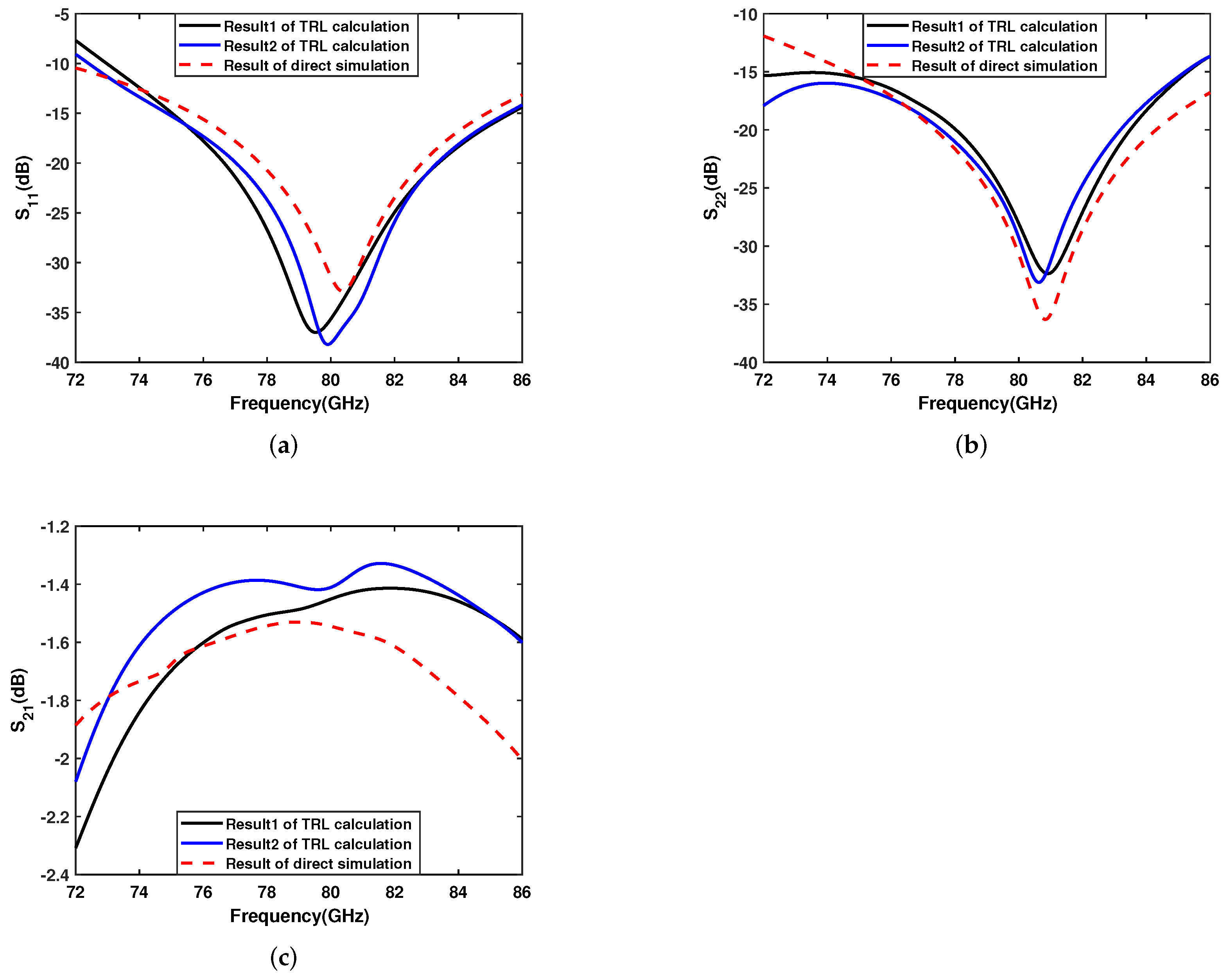
After getting these S parameters, we can calculate the parameters of the package-board transition through the TRL technology described in Section 4.2. The calculation and direct simulation results are shown in Figure 19. The CPW on the RDL and the GCPW on the test board used in the TRL technique are longer than that in the port reduction technique, so the calculated S parameter is different from the S parameter calculated by the port reduction technique. Result 1 and Result 2 of the TRL calculation are calculated using the S parameters of thru 1 and thru 2, respectively. They are roughly the same, but there are some differences. This tells us that we need to ensure the consistency of the electromagnetic environment as much as possible when designing the experiment. We can find that whether it is reflection coefficient or transmission coefficient, the results calculated by the TRL method and the results obtained by the direct simulation show a relatively high consistency. Therefore, the feasibility of the TRL method is verified.
6. Conclusions
In this paper, a well-matched package-board transition has been designed by using the impedance converter. The simulated insertion loss for the transition is about 0.82 dB at 79 GHz, and the simulated return loss is better than 10 dB from 72 GHz to 86 GHz. The ceramic substrate has been chosen as the test board. Thus, the probe can touch the GCPW lines on the test board directly. In order to solve the challenge of obtaining the measured S-parameter matrix of the package-board transition, two different measurement methods based on the port reduction technique and the TRL technique have been proposed. We analyzed the principles of the two methods and designed the corresponding test structures. At the same time, we verified the feasibility of the two methods by simulation. The results calculated by these two methods are basically the same as the direct simulation results. All the simulation ports used in the two methods can be mapped to actual test ports. Thus, we can measure at the corresponding ports and then calculate the S-parameter matrix of the transition through the two methods. FOWLP and test board samples have been fabricated, and the sample of the FOWLP has been soldered on the test board successfully. The following research work will further verify the two methods through experiments.
Author Contributions
Software, writing original draft, investigation, and methodology, Y.C.; writing—review and editing, Y.C. and J.L.; project administration, J.L.; supervision, L.C. All authors have read and agreed to the published version of the manuscript.
Funding
This research was funded by [the National Natural Science Foundation of China] grant number [U21A20504].
Data Availability Statement
The data presented in this study are available on request from the corresponding author. The data are not publicly available due to privacy.
Conflicts of Interest
The authors declare no conflict of interest.
References
- Hedler, H.; Meyer, T.; Vasquez, B. Transfer Wafer Level Packaging. U.S. Patent US6727576 B2, 27 April 2004. [Google Scholar]
- Keser, B.; Kroehnert, S. Advances in Embedded and Fan-Out Wafer Level Packaging Technologies; Wiley-IEEE Press: Piscataway, NJ, USA, 2019; p. 51. [Google Scholar]
- Liu, D.; Zhang, Y. Antenna-in-Package Technology and Applications; Wiley-IEEE Press: Piscataway, NJ, USA, 2020; p. 219. [Google Scholar]
- Wu, D.; Dahlback, R.; Ojefors, E.; Carlsson, M.; Yoon, S.W. Advanced Wafer Level PKG Solutions for 60 GHz WiGig (802.11ad) Telecom Infrastructure. In Proceedings of the 2019 IEEE 69th Electronic Components and Technology Conference (ECTC), Las Vegas, NV, USA, 28–31 May 2019; pp. 968–971. [Google Scholar]
- Hartner, W.; Niessner, M.; Arcioni, F.; Fink, M.; Wojnowski, M. Reliability and Performance of Wafer Level Fan Out Package for Automotive Radar. In Proceedings of the 2019 International Wafer Level Packaging Conference (IWLPC), San Jose, CA, USA, 22–24 October 2019; pp. 1–11. [Google Scholar]
- Agethen, R.; PourMousavi, M.; Forstner, H.P.; Wojnowski, M.; Pressel, K.; Weigel, R.; Kissinger, D. 60 GHz industrial radar systems in silicon-germanium technology. In Proceedings of the 2013 IEEE MTT-S International Microwave Symposium Digest (MTT), Seattle, WA, USA, 2–7 June 2013; pp. 1–3. [Google Scholar]
- Beck, C.; Ng, H.J.; Agethen, R.; Pourmousavi, M.; Forstner, H.P.; Wojnowski, M.; Pressel, K.; Weigel, R.; Hagelauer, A.; Kissinger, D. Industrial mmWave Radar Sensor in Embedded Wafer-Level BGA Packaging Technology. IEEE Sens. J. 2016, 16, 6566–6578. [Google Scholar] [CrossRef]
- Nasr, I.; Jungmaier, R.; Baheti, A.; Noppeney, D.; Trotta, S. A Highly Integrated 60 GHz 6-Channel Transceiver with Antenna in Package for Smart Sensing and Short-Range Communications. IEEE J. Solid-State Circuits 2016, 51, 2066–2077. [Google Scholar] [CrossRef]
- Keser, B.; Amrine, C.; Duong, T.; Fay, O.; Wenzel, R. The Redistributed Chip Package: A Breakthrough for Advanced Packaging. In Proceedings of the 2007 IEEE 57th Electronic Components and Technology Conference (ECTC), Sparks, NV, USA, 29 May–1 June 2007; pp. 286–291. [Google Scholar]
- Kripesh, V.; Rao, V.S.; Kumar, A.; Sharma, G.; Lau, J. Design and development of a multi-die embedded micro wafer level package. In Proceedings of the 2008 IEEE 58th Electronic Components and Technology Conference (ECTC), Lake Buena Vista, FL, USA, 27–30 May 2008; pp. 1544–1549. [Google Scholar]
- Kumar, A.; Xia, D.; Sekhar, V.N.; Lim, S.; Keng, C.; Sharma, G.; Rao, V.S.; Kripesh, V.; Lau, J.H.; Kwong, D.L. Wafer level embedding technology for 3D wafer level embedded package. In Proceedings of the 2009 IEEE 59th Electronic Components and Technology Conference (ECTC), San Diego, CA, USA, 26–29 May 2009; pp. 1289–1296. [Google Scholar]
- Yoon, S.W.; Caparas, J.A.; Lin, Y.; Marimuthu, P.C. Advanced low profile PoP solution with embedded wafer level PoP (eWLB-PoP) technology. In Proceedings of the 2012 IEEE 62nd Electronic Components and Technology Conference (ECTC), San Diego, CA, USA, 29 May–1 June 2012; pp. 1250–1254. [Google Scholar]
- Tseng, C.F.; Liu, C.S.; Wu, C.H.; Yu, D. InFO (Wafer Level Integrated Fan-Out) Technology. In Proceedings of the 2016 IEEE 66th Electronic Components and Technology Conference (ECTC), Las Vegas, NV, USA, 31 May–3 June 2016; pp. 1–6. [Google Scholar]
- Hsieh, C.C.; Wu, C.H.; Yu, D. Analysis and Comparison of Thermal Performance of Advanced Packaging Technologies for State-of-the-Art Mobile Applications. In Proceedings of the 2016 IEEE 66th Electronic Components and Technology Conference (ECTC), Las Vegas, NV, USA, 31 May–3 June 2016; pp. 1430–1438. [Google Scholar]
- Wojnowski, M.; Pressel, K.; Beer, G.; Heinig, A. Vertical interconnections using through encapsulant via (TEV) and through silicon via (TSV) for high-frequency system-in-package integration. In Proceedings of the 2014 IEEE 16th Electronics Packaging Technology Conference (EPTC), Singapore, 3–5 December 2014; pp. 122–127. [Google Scholar]
- Lau, J.H.; Li, M.; Li, Q.M.; Chen, T.; Xu, I.; Yong, Q.X. Fan-Out Wafer-Level Packaging for Heterogeneous Integration. IEEE Trans. Compon. Packag. Manuf. Technol. 2018, 8, 1544–1560. [Google Scholar] [CrossRef]
- Chen, C.; Yu, D.; Wang, T.; Xiao, Z.; Wan, L. Warpage Prediction and Optimization for Embedded Silicon Fan-Out Wafer-Level Packaging Based on an Extended Theoretical Model. IEEE Trans. Compon. Packag. Manuf. Technol. 2019, 9, 845–853. [Google Scholar] [CrossRef]
- Fowler, M.; Massey, J.P.; Braun, T.; Voges, S.; Wohrmann, M. Investigation and Methods Using Various Release and Thermoplastic Bonding Materials to Reduce Die Shift and Wafer Warpage for eWLB Chip-First Processes. In Proceedings of the 2019 IEEE 69th Electronic Components and Technology Conference (ECTC), Las Vegas, NV, USA, 28–31 May 2019; pp. 363–369. [Google Scholar]
- Wu, M.L.; Lan, J.S. Simulation and Experimental Study of the Warpage of Fan-Out Wafer-Level Packaging: The Effect of the Manufacturing Process and Optimal Design. IEEE Trans. Compon. Packag. Manuf. Technol. 2019, 9, 1396–1405. [Google Scholar] [CrossRef]
- Lau, J.H.; Li, M.; Yang, L.; Li, M.; Xu, I.; Chen, T.; Chen, S.; Yong, Q.X.; Madhukumar, J.P.; Kai, W.; et al. Warpage Measurements and Characterizations of Fan-Out Wafer-Level Packaging With Large Chips and Multiple Redistributed Layers. IEEE Trans. Compon. Packag. Manuf. Technol. 2018, 8, 1729–1737. [Google Scholar] [CrossRef]
- Shih, M.K.; Huang, C.Y.; Chen, T.H.; Wang, C.C.; Tarng, D.; Hung, C.P. Electrical, Thermal, and Mechanical Characterization of eWLB, Fully Molded Fan-Out Package, and Fan-Out Chip Last Package. IEEE Trans. Compon. Packag. Manuf. Technol. 2019, 9, 1765–1775. [Google Scholar] [CrossRef]
- Lau, J.H.; Ming, L.; Tian, D.; Fan, N.; Yong, Q. Warpage and Thermal Characterization of Fan-Out Wafer-Level Packaging. IEEE Trans. Compon. Packag. Manuf. Technol. 2017, 7, 1729–1738. [Google Scholar] [CrossRef]
- Dong, H.; Chen, J.; Hou, D.; Xiang, Y.; Hong, W. A Low-Loss Fan-Out Wafer-Level Package with a Novel Redistribution Layer Pattern and Its Measurement Methodology for Millimeter-Wave Application. IEEE Trans. Compon. Packag. Manuf. Technol. 2020, 10, 1073–1078. [Google Scholar] [CrossRef]
- Wojnowski, M.; Pressel, K.; Beer, G.; Heinig, A. Co-Design of High-Isolation Chip-Package-Board in eWLB Package for 77 GHz Automotive Radar Application. In Proceedings of the 2019 IEEE 21st Electronics Packaging Technology Conference (EPTC), Singapore, 4–6 December 2019; pp. 519–522. [Google Scholar]
- Zhu, C.; Duan, Z.; Dai, Y. Design of CMOS Chip to Waveguide Transition in eWLB Package for Full W-band Applications. In Proceedings of the 2020 IEEE MTT-S International Microwave Workshop Series on Advanced Materials and Processes for RF and THz Applications (IMWS-AMP), Suzhou, China, 29–31 July 2020; pp. 1–3. [Google Scholar]
- Huynh, N.H.; Saverio, T.; Wojnowski, M.; Haubner, G. eWLB package for millimeter wave application. In Proceedings of the 2015 European Microelectronics Packaging Conference (EMPC), Friedrichshafen, Germany, 14–16 September 2015; pp. 1–5. [Google Scholar]
- Henawy, M.A.; Schneider, M. Integrated antennas in eWLB packages for 77 GHz and 79 GHz automotive radar sensors. In Proceedings of the 2011 41st European Microwave Conference, Manchester, UK, 10–13 October 2011; pp. 1312–1315. [Google Scholar]
- Wojnowski, M.; Sommer, G.; Klumpp, A.; Weber, W. Electrical Characterization of 3D Interconnection Structures up to Millimeter Wave Frequencies. In Proceedings of the 2008 10th Electronics Packaging Technology Conference, Singapore, 9–12 December 2008; pp. 1393–1402. [Google Scholar]
- Hernandez-Sosa, G.; Romo, G.; Torres-Torres, R. Characterization and modeling of electronic packages using S-parameters. In Proceedings of the 2008 7th International Caribbean Conference on Devices, Circuits and Systems, Cancun, Mexico, 28–30 April 2008; pp. 1–6. [Google Scholar]
- Engl, M.; Schiller, K.; Eurskens, W.; Weigel, R. High resolution time domain and frequency domain package characterization up to 65 GHz. In Proceedings of the 56th Electronic Components and Technology Conference 2006 (ECTC), San Diego, CA, USA, 30 May–2 June 2006; pp. 7–13. [Google Scholar]
- Lu, H.C.; Chu, T.H. Port reduction methods for scattering matrix measurement of an n-port network. IEEE Trans. Microw. Theory Tech. 2000, 48, 959–968. [Google Scholar]
- Engen, G.F.; Hoer, C.A. Thru-Reflect-Line: An Improved Technique for Calibrating the Dual Six-Port Automatic Network Analyzer. IEEE Trans. Microw. Theory Tech. 1979, 27, 987–993. [Google Scholar] [CrossRef] [Green Version]
- Marks, R.B. A multiline method of network analyzer calibration. IEEE Trans. Microw. Theory Tech. 1991, 39, 1205–1215. [Google Scholar] [CrossRef] [Green Version]
- Chen, Y.; Li, J.; Ding, F.; Cao, L. Antenna in package design and measurement for millimeter-wave applications in fan-out wafer-level package. IEICE Electron. Express 2022. advance online publication. [Google Scholar] [CrossRef]
Figure 1.
Cross-section of the FOWLP structure. Reprinted with permission from [34]. 2022, IEICE.
Figure 1.
Cross-section of the FOWLP structure. Reprinted with permission from [34]. 2022, IEICE.

Figure 2.
Process flow of the RDL-First FOWLP. Reprinted with permission from [34]. 2022, IEICE.
Figure 2.
Process flow of the RDL-First FOWLP. Reprinted with permission from [34]. 2022, IEICE.
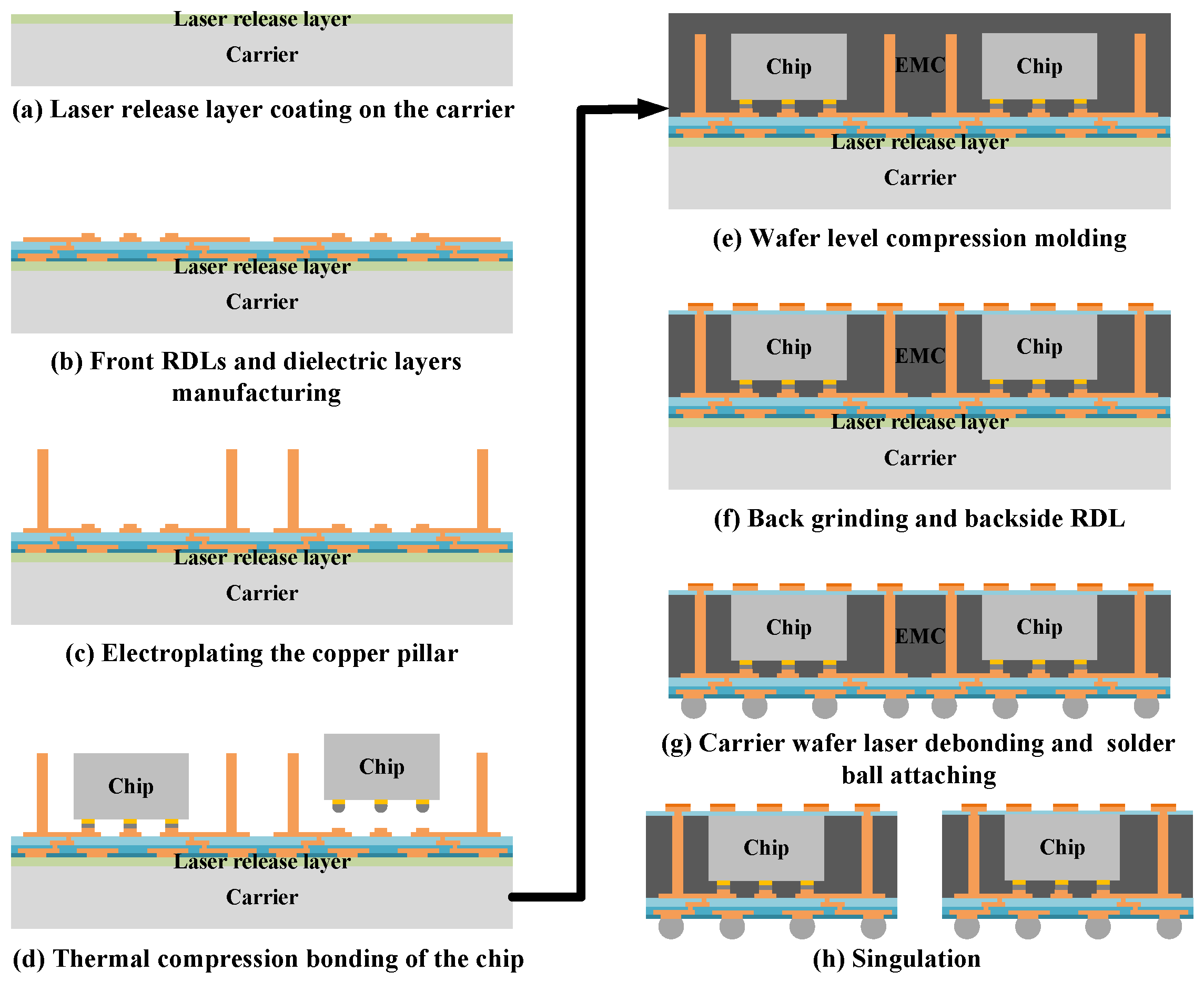
Figure 3.
Three-dimensional simulation model for the package-board transition.
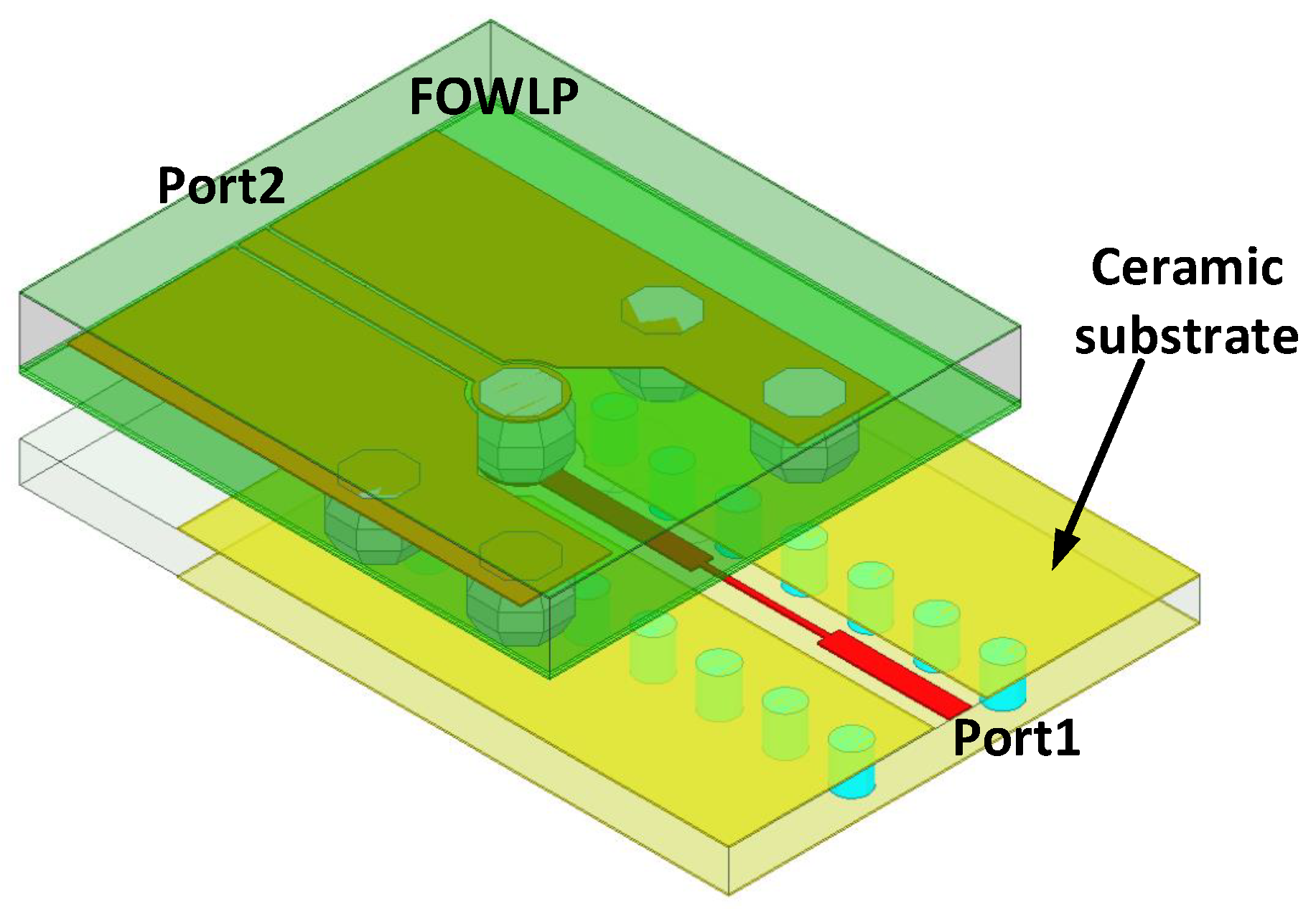
Figure 4.
Top view of the ceramic substrate for the transition (Units: mm).
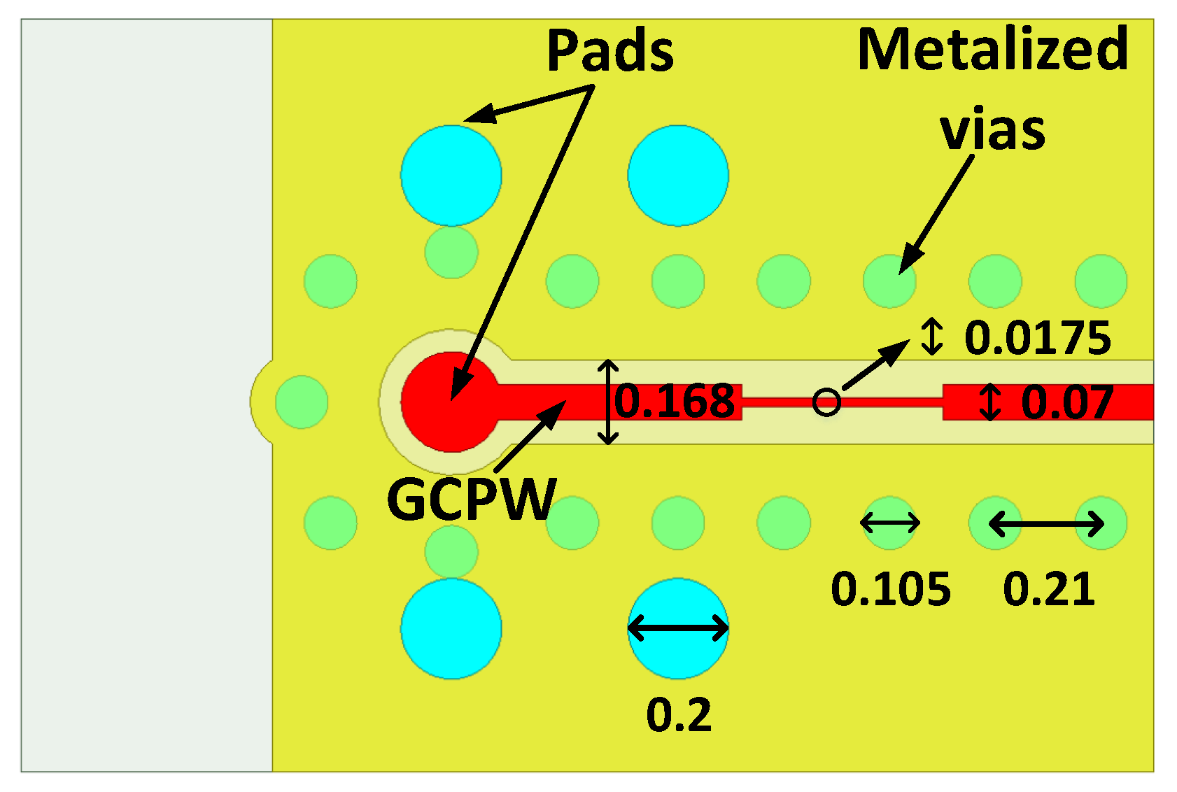
Figure 5.
Simulation results of the package-board transition. (a) S or S, (b) S or S.
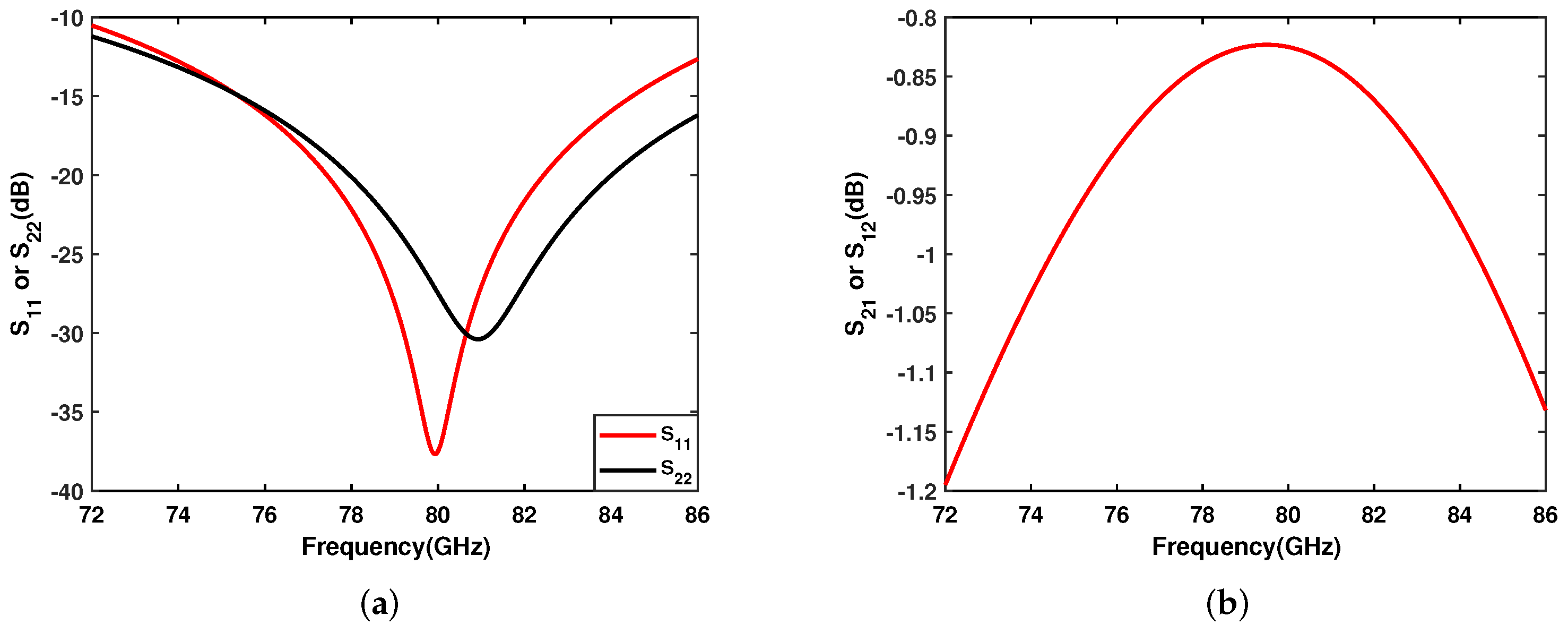
Figure 6.
Block diagram of the single port test.

Figure 7.
Top view of the simulation model for the single port test.

Figure 8.
Test block diagram based on the TRL calibration technique.
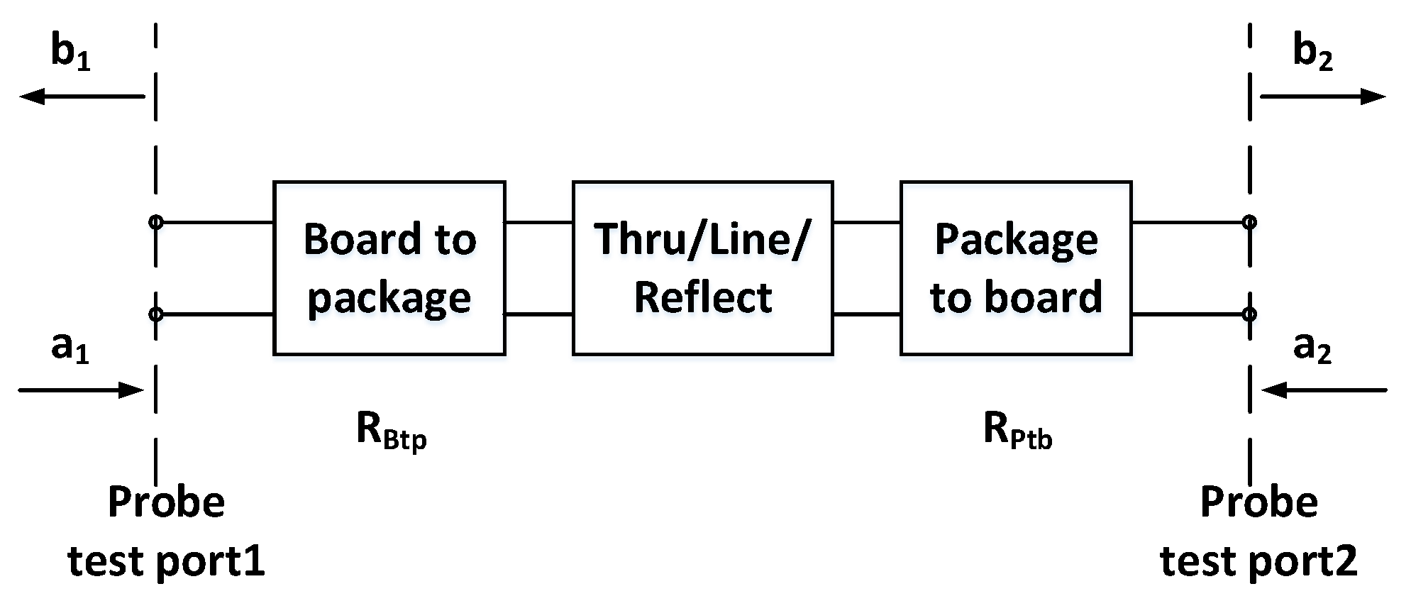
Figure 9.
Simulation models of the thru/delay line/reflect structure. (a) Thru, delay line structure. (b) Reflect structure.
Figure 9.
Simulation models of the thru/delay line/reflect structure. (a) Thru, delay line structure. (b) Reflect structure.
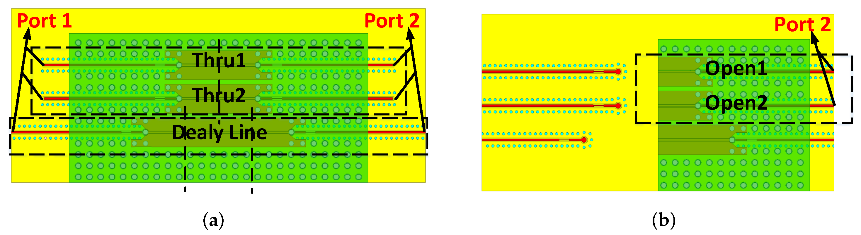
Figure 10.
Photo of the fabricated sample of the FOWLP. (a) Front side. (b) Back side.

Figure 11.
FOWLP soldered on the ceramic substrate.
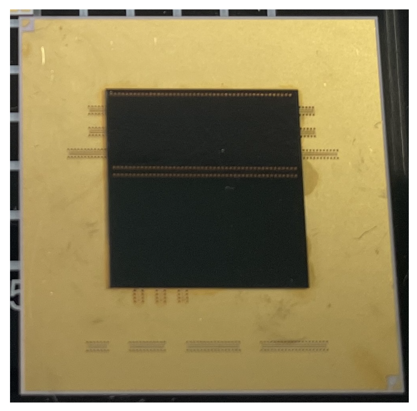
Figure 12.
Three-dimensional model of the designed structures for the port reduction technology. (a) Model without test board, (b) model with test board.
Figure 12.
Three-dimensional model of the designed structures for the port reduction technology. (a) Model without test board, (b) model with test board.
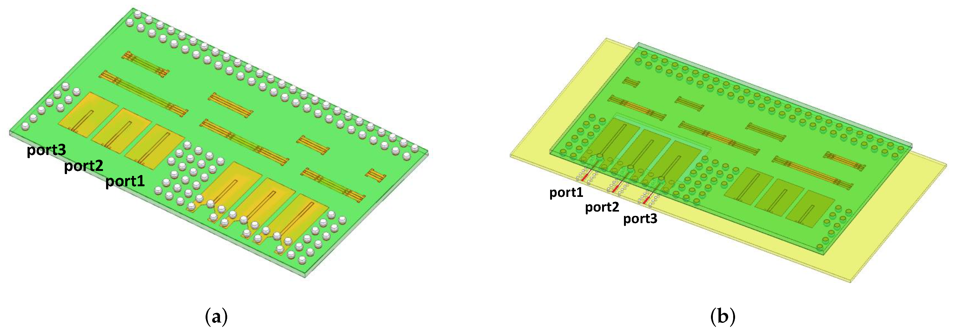
Figure 13.
Simulated S (a) at reference plane B, (b) at reference plane A.
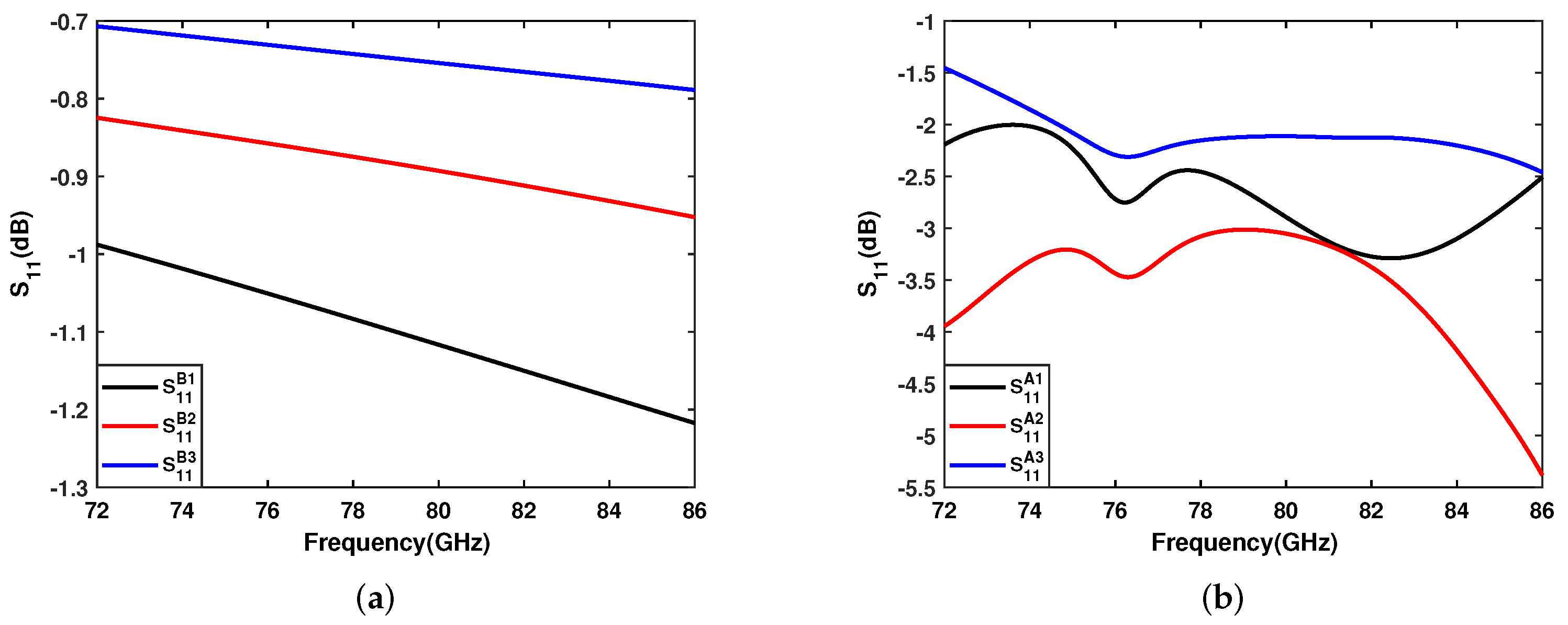
Figure 14.
Three-dimensional model of the direct simulation for the package-board transition.
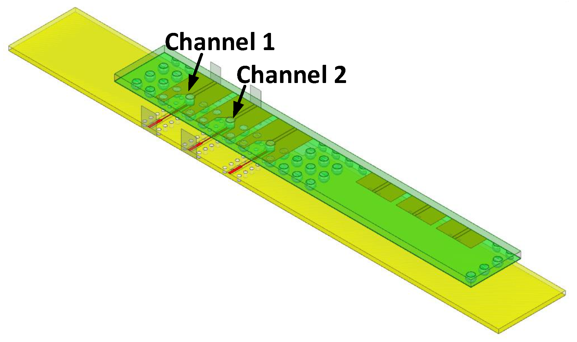
Figure 15.
Comparison of the package-board transition results calculated by the port reduction method and the direct simulation results. (a) S, (b) S, (c) S/S.
Figure 15.
Comparison of the package-board transition results calculated by the port reduction method and the direct simulation results. (a) S, (b) S, (c) S/S.

Figure 16.
S parameters of the designed thru structure. (a) S or S, (b) S or S.

Figure 17.
S parameters of the designed delay line structure. (a) S or S, (b) S or S.
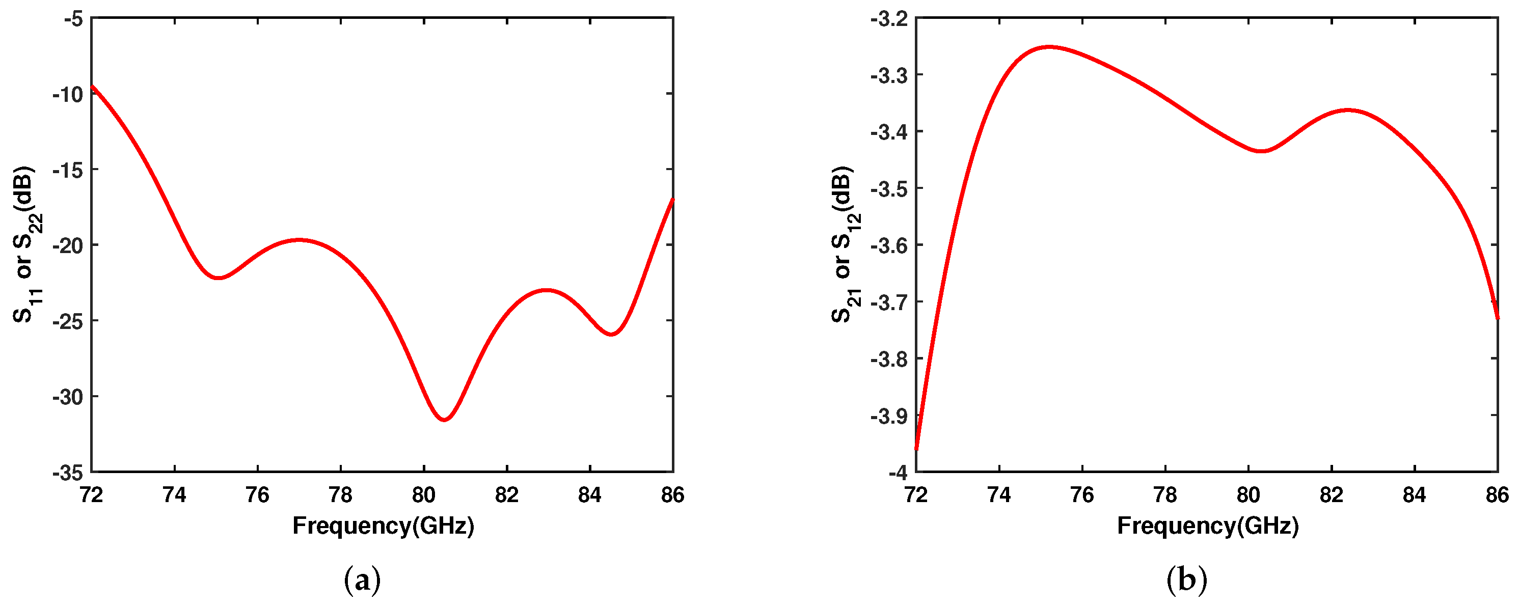
Figure 18.
S of the designed open structure.
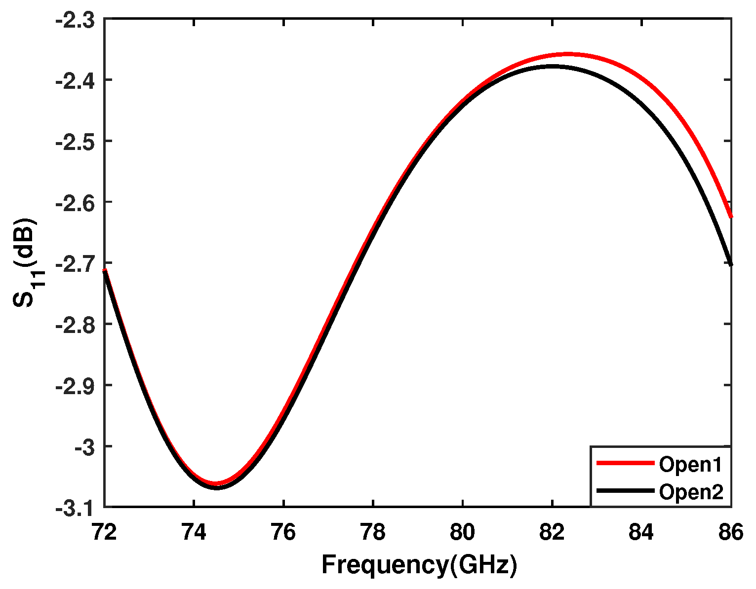
Figure 19.
Comparison of the package-board transition results calculated by the TRL method and the direct simulation results. (a) S, (b) S, (c) S/S.
Figure 19.
Comparison of the package-board transition results calculated by the TRL method and the direct simulation results. (a) S, (b) S, (c) S/S.
Publisher’s Note: MDPI stays neutral with regard to jurisdictional claims in published maps and institutional affiliations. |
© 2022 by the authors. Licensee MDPI, Basel, Switzerland. This article is an open access article distributed under the terms and conditions of the Creative Commons Attribution (CC BY) license (https://creativecommons.org/licenses/by/4.0/).
Share and Cite
MDPI and ACS Style
Chen, Y.; Li, J.; Cao, L. Design for the Package-Board Transition and Its Testability Design in the Fan-Out Wafer-Level Package. Electronics 2022, 11, 1922. https://doi.org/10.3390/electronics11121922
AMA Style
Chen Y, Li J, Cao L. Design for the Package-Board Transition and Its Testability Design in the Fan-Out Wafer-Level Package. Electronics. 2022; 11(12):1922. https://doi.org/10.3390/electronics11121922
Chicago/Turabian StyleChen, Ying, Jun Li, and Liqiang Cao. 2022. "Design for the Package-Board Transition and Its Testability Design in the Fan-Out Wafer-Level Package" Electronics 11, no. 12: 1922. https://doi.org/10.3390/electronics11121922
Note that from the first issue of 2016, this journal uses article numbers instead of page numbers. See further details here.