
A High Performance 0.18 μm RF Switch for Multi-Standard

1
Institute of Microelectronics of the Chinese Academy of Sciences, Beijing 100029, China
2
University of Chinese Academy of Sciences, Beijing 100049, China
3
Hangzhou Zhongke Microelectronics Co., Ltd, Hangzhou 310053, China
*
Author to whom correspondence should be addressed.
Electronics 2022, 11(13), 2046; https://doi.org/10.3390/electronics11132046
Submission received: 7 June 2022
/
Revised: 22 June 2022
/
Accepted: 27 June 2022
/
Published: 29 June 2022
(This article belongs to the Section Microelectronics)
Abstract
:This paper proposes a stacked field-effect transistor (FET) single-pole, double-throw (SPDT) RF switch which is capable of multi-standard. Negative voltage generator (NVG), logic controller, level shifter, and RF Switch branches are integrated. A PMOS self-biased strategy is proposed to improve linearity and simplify the design of the logic controller and level shifter. In order to reduce the influence of NVG, a new charge pump (CP) is proposed, and a low pass filter (LPF) is added to stabilize bias voltages. A new layout of the switch FET is proposed to minimize the product of on-state resistance and off-state capacitance (time constant). The RF switch proposed in this paper was implemented in the 0.18 μm silicon on insulator (SOI) process. The measured results show the P1 dB of 40 dBm, and the isolation (ISO) and insert loss (IL) at 1 GHz/5 GHz of 37 dB/22 dB, and 0.36 dB/0.55 dB. The operating frequency range is DC-6 GHz. Supply current is 37uA with the supply voltage of 2.6V.
1. Introduction
RF switch is important in RF front-end modules. Different communication standards focus on different merits, the key requirements of the RF antenna switches for GSM, WIFI (802.11x) and WCDMA are listed in Table 1. To cover the different standards, we must achieve a trade-off on these parameters, which is difficult.
A lot of work has been done to improve the performance of the RF switch. Many of those works are implemented in SOI or bulk CMOS process, The two processes are similar, but the former offers better ISO by adding Buried Oxide(BOX) Layer to reduce the leakage current. The optimization methods for these two processes are similar. To improve the power capacity of switches, [1,2,3] adopted a floating-body structure in the CMOS process, a resistor is added between the ground and the body terminal of the transistor, The results in [4] show that the P1 dB of the floating-body switch is 5 dB better than that of the traditional one. Similarly, [5] adopted the same structure in the SOI process, but the resistor is not needed because of the resistance of the BOX layer in large. The LC tuning technique is used in [6] to improve the power handling capacity by reducing the parasitic capacitance of transistors, but the frequency of the switch is limited. Apart from those, there have been a lot of attempts made to achieve high-power switches with SOI or CMOS processes, such as using negative supply voltage to the body substrate [7,8,9,10,11], differential switch structure [12,13], Asymmetric branches [6,14,15,16], and feedforward capacitors [6,17,18] is adopted to address the issue of the unequal voltage division caused by the Asymmetric parasitic capacitance of switch FETs.
In addition to SOI and bulk CMOS processes, there are some other processes adopted. For example, the SiGe HBT process is used for a high-frequency application, and the working frequency of the switch proposed in [19] is dc-110 GHz. MEMS technology is used in RF switch design owing to its reduced size, low power consumption, and superior RF response. However, its reliability issues need to be considered [20,21].
Some works proposed the new structures of the switch. The classical series-parallel structure can improve the performance of the switch, but when the operating frequency exceeds 10 GHz, the parasitic capacitance of the parallel path deteriorates IL. To solve this problem, [22] proposed a switch structure without parallel branches and adjusted the layout of the switch FET to further reduce the effect of parasitic capacitance.
In addition to the optimization of RF switches alone, there are some works that design RF switches together with other modules, such as ESD [23,24], antenna [13], impedance matching networks [12] and NVG [25,26,27]. The performance of RF switches in these works is not outstanding, but the whole module can achieve good performance.
In this paper, a PMOS self-biased RF switch with a reduced time constant and a new NVG block is designed and implemented in the 0.18 μm SOI process. Section 2 introduces the blocks of RF switch. A PMOS self-biased strategy is proposed to minimize the nonlinear capacitance which degrades power capacity. To stabilize bias voltages, a new CP is proposed and an LPF is added at the output of the low dropout regulator (LDO). The parasitic resistance and capacitance of FET are analyzed, and a method to reduce the time constant is given, the proposed layout of FET is designed accordingly.
2. SOI SPDT Switch Design
2.1. Biasing Strategy
The performance of the switch is strongly dependent on biasing strategy. Traditional FB-FETs biasing technique utilizes the buried oxide (BOX) layer of SOI FETs, leaving a floating body of FET [7,28]. But the nonlinear capacitance degrades power capacity badly when the switch FET is turned off. The junction capacitance is the main component of nonlinear capacitance, and it is given in (1):
where is the reverse voltage across the junction, is the junction built-in potential, and m is a power typically in the range of 0.3 and 0.4. can be reduced by improving the absolute value of , which indicates the source/drain-body junction of FET should be strongly reverse biased in off-state.
A self-biased PMOS strategy is proposed in this work, and a circuit of RF switch branches is shown in Figure 1. The self-biased PMOS is added between the gates and source of each FET switch. The gates of FET switches in the serial path are biased at a positive voltage in on-state, so, the PMOS is turned off for being reverse biased, and the body of the FET is biased close to the ground because the source/drain-body parasitic diodes are slightly reverse biased. While switch FET is turned off, the gate of the FET is biased at a negative voltage, and the PMOS of it is turned on, the body of FETs are biased to a negative voltage. Additional bias voltages are not needed in the design. In conclusion, the proposed biasing strategy improves power capacity by reducing nonlinear capacitance and the number of bias voltages is just the same as FB-FETs biasing technique.
2.2. Circuit of NVG
NVG is necessary because the negative bias voltage is required in the self-biased PMOS biasing strategy. CP is widely used in NVG, the circuit of traditional CP is shown in Figure 2, charge1 and discharge1 are the charging path and discharging path when CLK is 0, and charge2 and discharge2 are that when CLK is 1.
The first problem of the traditional CP is the leakage current, which happens when the PMOS and NMOS, such as MN2 and MP2 shown in Figure 2, are simultaneously turned on for a short time at the transitions of CLK. This results in higher power consumption and the degradation of output voltage. Figure 3 is used to illustrate the influence of the leakage current, and are the voltages of drain and gate of MN3 and MP3, MN3 works in triode region from 0 to t1, and works in saturation region from t1 to t2, the duration of the transition is t0. The power consumption introduced by the overlapping of CLK1 and CLK2 is given in (2) [27]:
where , . For the situation that the PMOS and NMOS are perfectly matched, , , (2) reduces to (3):
Another problem is the asymmetry of CLK and NCLK (a transmission gate is adopted in this design to reduce the asymmetry). In Figure 4 are the simulation results of traditional CP, the asymmetry between B and C is even worse than that of CLK and NCLK. As a result, the discharge1 and discharge2 paths are turned on at the same time between t1 and t2 shown in Figure 3 when CLK falls, so the discharging current is larger and the fluctuation of the output voltage is worse. Similarly, the charge1 and charge2 paths are turned on at the same time when CLK rises. As a result, the voltage fluctuations on the rising and falling edges of the CLK are different. The simulation results shown in Figure 5 also prove this. (The timing of the rising edge of CLK is changed to place the curves in the same graph for comparison).
To solve those problems, a new CP with four-phase non-overlapping clocks is proposed. As shown in the Figure 6, the CP consists of three CPs, two of which are auxiliary CPs, they are used to convert the four-phase clocks into the control signals of the main CP. The auxiliary CPs adopt the structure of traditional CP, but since the transistors and capacitors in auxiliary CPs are much smaller than that of the main charge pump, its effect on the output voltage is negligible. Figure 7 is the timing diagram of non-overlapping clocks. Due to the phase differences (p1 and p2), the PMOS and NMOS, such as PM2 and NM2, will not be turned on at the same time. The simulation results of the proposed CP are given in Figure 5, The output voltage of the proposed charge pump produces much less fluctuation than the conventional charge pump, and the output voltage is also closer to -VDD.
The diagram of the RF switch chip is given in Figure 8. The oscillator and the four-phase non-overlapping clocks generator induce glitches in positive bias voltage. To minimize the influence of this process, a LPF is added between V1 and V2.
The post-simulation results in Figure 9 show the negative voltage with and without the proposed CP, and Figure 10 show the fluctuation in the input and output voltage of the added LPF. It can be seen from the results that the fluctuation in the bias voltages of the proposed circuit is neglectable compared to that of the traditional circuit. is also small compared. The effectiveness of the proposed CP and the added LPF is proved.
2.3. Reduced Time Constant
2.3.1. Analysis of IL and ISO
The equivalent-circuit of RF switch is shown in Figure 11. Suppose the width of the FETs in the series and the shunt branch are w and separately, then the and of shunt branch are and . The IL is given in (4) and is simplified as (5). The is neglectable compared to () because is smaller than 100fF. Equation (3) indicates that the IL is mainly depended on , reducing produces better IL. ISO is given in (6), and it can be simplified as (7), so ISO is related with , and .
ISO can be improved with greater because the larger size of the shunt switch FETs will reduce the . But, increases, the performance of the harmonic degrades as a result, and a larger chip area is required.
2.3.2. FET with Reduced Time Constant
IL and ISO can be improved by reducing and respectively according to Equations (5) and (7). The cross section of FET is established in Figure 12, only metal1 and metal2 are taken into consideration here. and can be reduced by adjusting process, but it is unavailable for circuit designers. The parasitic capacitance between metal wire strongly depends on the layout of components, parasitic capacitance can be reduced with better layout. Equation (8):
is the total off-capacitance of a FET according to Figure 12, where Cp is the capacitance related with process, and is the capacitance introduced by metal wire. is consisted of and , and is composed of the capacitance between contact and gate (), metal1 and gate (), metal1 and metal1 (), metal2 and metal2 (), metal1 and metal2 ().
To reduce the parasitic capacitance between metals, the area between metals should be reduced. To keep the same current density, Metal1 should not be adjusted. And Metal2, as the connection line between devices, is shortenable. According to this, the traditional layout and proposed layout were shown in Figure 13, the metal2 wire in the proposed layout is shorter than the traditional one. Ignoring the , and , is the capacitance of per unit length of . The off-state capacitance of the traditional layout () and the proposed layout () is expressed as (9) and (10) according to (8).
As for Ron, it is given in (11):
is the resistance of channel, and Rpar is everything else, in which the resistance of M1 (), M2 (), via () and contact () are taken into consideration here. The num-ber of vias and contacts are n and m, and they are set to be 12 and 15 in this work. The resistance of a single contact and a single via are and . Ron for traditional layout () and proposed layout () are calculated with (12) and (13).
In Table 2 are the parameters of the adopted process. Because the resistance introduced by via is small, the increase in on-resistance has a negligible effect on performance. But the parasitic capacitance is reduced by 12.06% according to (9), (10) and Table 2. As shown in the Figure 14, the ISO at 5 GHz of the switch with proposed layout is 1.5 dB better than that of the switch with traditional layout, and the degration of IL is negenactable. The improvement of ISO caculated with the 12.05% reduced parasitic capacitance is 1 dB, the difference is expected to result from the neglected capacitance in Equations (9) and (10).
3. Measured Results
The photo of the fabricated chip is given in Figure 15. The RF Switch propoesd in this work was designed and implemented in 0.18 μm SOI process. The total area of the chip is mm with two branches, an NVG block, a level-shifter, a logic controller, and the surrounding pads and ESD circuits integrated. The rated operating voltage is 3 V, the output of LDO is 2.35 V, and the output of NVG is closed to −2.35 V. The control voltage is 2.6 V/0 V. The measured total supply current is 37 μA. The measurement results are calibrated with the thru-line loss of the PCB traces and SMA connectors [29].
Figure 16, Figure 17 and Figure 18 are measurement results of the proposed RF switch. The switch achieves the IL and ISO of 0.31 dB/0.6 dB and 55 dB/18 dB at 100 MHz/6 GHz. In the operating frequency band of DC-6 GHz, the IL is better than 0.6 dB and the ISO is better than 18 dB for both branches. The measured 3rd harmonic power () is shown in Figure 19, and the measured is shown in Figure 18. The RF switch can handle the input power of 39.5 dBm. In Table 3, the comparison of the proposed RF switch and published works are shown.
Table 3 shows the comparison of the proposed RF switch and the published works. The proposed RF switch shows comparable bandwidth, ISO, and IL while the operating frequency range is markedly better than that of other works, the overall performance of the proposed RF switch is excellent in the frequency range of 1–6 GHz. In terms of power consumption, because the NVG module is used in this paper, the power consumption is significantly higher than the work without NVG, but the supply current is the lowest in the RF switches that use the NVG module. Comparing with the literature using the CMOS process, it can be seen that the RF switches using the SOI process have significant improvements in ISO and .
4. Conclusions
In this paper, a PMOS self-biased RF switch is proposed. The number of biased voltages is the same as that of the FB-FETs biasing technique. By biasing the body terminal of the switch FETs at negative voltage in off state, the power capacity is increased to 39.5 dBm which is good enough for many wireless standards. A new CP is proposed and an LPF was added to stable the bias voltages, the post-layout simulation results verify the effectiveness of proposed CP and the added LPF. The factors influencing ISO and IL are analyzed, and the layout of FET has been improved based on the analysis results. The post-layout simulation results show that the ISO of the RF switch with the proposed layout is 1.5 dB better than that of the traditional one at 5 GHz. The measured results and the comparison with published works indicate that the proposed RF switch achieves a trade-off, and is capable of industry-standard results.
Author Contributions
Conceptualization, W.L. and Y.G.; methodology, W.L.; validation, Y.G.; formal analysis, W.L.; investigation, W.L.; data curation, W.L.; writing—original draft preparation, W.L.; writing—review and editing, Y.G.; project administration, Y.G. All authors have read and agreed to the published version of the manuscript.
Funding
This research received no external funding.
Data Availability Statement
No new data was created or analyzed in this study. Data sharing is not applicable to this paper.
Conflicts of Interest
The authors declare no conflict of interest.
References
- Truong, T.K.N.; Lee, D.S.; Lee, K.Y. A Low Insertion-Loss, High-Isolation Switch Based on Single Pole Double Throw for 2.4 GHz BLE Applications. IEIE Trans. Smart Process. Comput. 2016, 5, 164–168. [Google Scholar] [CrossRef] [Green Version]
- Yeh, M.-C.; Tsai, Z.-M.; Liu, R.-C.; Lin, K.Y.; Chang, Y.-T.; Wang, H. Design and analysis for a miniature CMOS SPDT switch using body-floating technique to improve power performance. IEEE Trans. Microw. Theory Tech. 2006, 54, 31–39. [Google Scholar] [CrossRef]
- Zhang, T.; Subramanian, V.; Boeck, G. Comparison of regular and floating bulk transistors in ultra-wideband CMOS T/R switches. In Proceedings of the 2012 19th International Conference on Microwaves, Radar & Wireless Communications, Warsaw, Poland, 21–23 May 2012; Volume 1, pp. 293–296. [Google Scholar] [CrossRef]
- Li, Z.; O, K. 15-GHz fully integrated nMOS switches in a 0.13-/spl mu/m CMOS process. IEEE J. Solid-State Circuits 2005, 40, 2323–2328. [Google Scholar] [CrossRef]
- Marian, V.; Verdier, J.; Allard, B.; Vollaire, C. Design of a wideband multi-standard antenna switch for wireless communication devices. Microelectron. J. 2011, 42, 790–797. [Google Scholar] [CrossRef]
- Wang, X.S.; Yue, C.P. A Dual-Band SP6T T/R Switch in SOI CMOS With 37-dBm P-0.1 dB for GSM/W-CDMA Handsets. IEEE Trans. Microw. Theory Tech. 2014, 62, 861–870. [Google Scholar] [CrossRef]
- Zhang, Z.; Zhang, G.; Yu, K.; Lin, J.; Huang, L. Effects and contrasts of silicon-on-insulator floating-body and body-contacted field-effect transistors to the design of high-performance antenna switches. IET Microwaves Antennas Propag. 2016, 10, 507–516. [Google Scholar] [CrossRef]
- Zhang, H.; Cui, Q.; Yan, X.; Shi, J.; Lin, F. A 0.5–3.0 GHz SP4T RF switch with improved body self-biasing technique in 130-nm SOI CMOS. J. Semicond. 2020, 41, 102404. [Google Scholar] [CrossRef]
- Im, D.; Lee, K. Characterization and optimization of partially depleted SOI MOSFETs for high power RF switch applications. Solid-State Electron. 2013, 90, 94–98. [Google Scholar] [CrossRef]
- Guan, H.; Sun, H.; Bao, J.; Wang, Z.; Zhou, S.; Zhu, H. High-performance RF Switch in 0.13 μm RF SOI process. J. Semicond. 2019, 40, 022401. [Google Scholar] [CrossRef]
- Zhang, Z.; Huang, L.; Yu, K.; Zhang, G. A novel body self-biased technique for enhanced RF performance of a SP8T antenna switch in partially depleted CMOS-SOI technology. In Proceedings of the 2014 12th IEEE International Conference on Solid-State and Integrated Circuit Technology (ICSICT), Guilin, China, 28–31 October 2014; pp. 1–3. [Google Scholar] [CrossRef]
- Kim, H.W.; Ahn, M.; Lee, O.; Kim, H.; Kim, H.; Lee, C.H. Analysis and Design of a Fully-Integrated High-Power Differential CMOS T/R Switch and Power Amplifier Using Multi-Section Impedance Transformation Technique. Electronics 2021, 10, 1028. [Google Scholar] [CrossRef]
- Zhang, Y.; Wang, J.; Li, Q.; Li, X. Antenna-in-Package and Transmit–Receive Switch for Single-Chip Radio Transceivers of Differential Architecture. IEEE Trans. Circuits Syst. I Regul. Pap. 2008, 55, 3564–3570. [Google Scholar] [CrossRef]
- Chen, L.; Gan, Y.B. An asymmetrical bulk cmos switch for 2.4 GHZ application. Prog. Electromagn. Res. Lett. 2017, 66, 99–104. [Google Scholar] [CrossRef] [Green Version]
- Bhandarkar, S.; Nakhate, S. Asymmetric Inductive Substrate bias RF SPDT Switch. Mater. Today Proc. 2017, 4, 10351–10355. [Google Scholar] [CrossRef]
- Li, Q.; Zhang, Y.P.; Yeo, K.S.; Lim, W.M. 16.6- and 28-GHz Fully Integrated CMOS RF Switches With Improved Body Floating. IEEE Trans. Microw. Theory Tech. 2008, 56, 339–345. [Google Scholar] [CrossRef]
- Ahn, M.; Kim, H.W.; Lee, C.H.; Laskar, J. A 1.8-GHz 33-dBm P 0.1-dB CMOS T/R Switch Using Stacked FETs With Feed-Forward Capacitors in a Floated Well Structure. IEEE Trans. Microw. Theory Tech. 2009, 57, 2661–2670. [Google Scholar] [CrossRef]
- Malladi, V.N.; Miller, M. A 48 dBm peak power RF switch in SOI process for 5G mMIMO applications. In Proceedings of the 2019 IEEE 19th Topical Meeting on Silicon Monolithic Integrated Circuits in RF Systems (SiRF), Orlando, FL, USA, 20–23 January 2019; pp. 1–3. [Google Scholar] [CrossRef]
- Cheon, C.D.; Cho, M.K.; Rao, S.G.; Cardoso, A.S.; Connor, J.D.; Cressler, J.D. A New Wideband, Low Insertion Loss SiGe Digital Step Attenuator A New Wideband, Low Insertion Loss SiGe Digital Step Attenuator. In Proceedings of the 2020 IEEE BiCMOS and Compound Semiconductor Integrated Circuits and Technology Symposium (BCICTS), Monterey, CA, USA, 16–19 November 2020; Volume 30, pp. 1–5. [Google Scholar] [CrossRef]
- Bansal, D.; Bajpai, A.; Kumar, P.; Kaur, M.; Kumar, A.; Chandran, A.; Rangra, K. Low voltage driven RF MEMS capacitive switch using reinforcement for reduced buckling. J. Micromechanics Microengineering 2017, 27, 024001. [Google Scholar] [CrossRef]
- Yamane, D.; Sun, W.; Seita, H.; Kawasaki, S.; Fujita, H.; Toshiyoshi, H. A Ku-band Dual-SPDT RF-MEMS Switch by Double-Side SOI Bulk Micromachining. J. Microelectromechanical Syst. 2011, 20, 1211–1221. [Google Scholar] [CrossRef]
- Li, Q.; Zhang, Y.P. CMOS T/R Switch Design: Towards Ultra-Wideband and Higher Frequency. IEEE J. Solid-State Circuits 2007, 42, 563–570. [Google Scholar] [CrossRef]
- Wang, X.S.; Wang, X.; Lu, F.; Zhang, C.; Dong, Z.; Wang, L.; Ma, R.; Shi, Z.; Wang, A.; Chang, M.C.F.; et al. Concurrent Design Analysis of High-Linearity SP10T Switch With 8.5 kV ESD Protection. IEEE J. Solid-State Circuits 2014, 49, 1927–1941. [Google Scholar] [CrossRef]
- Chen, A. Highly integrated CMOS RF SPDT switch with ESD and unit cell optimisation in MCM. Electron. Lett. 2013, 49, 549–551. [Google Scholar] [CrossRef] [Green Version]
- Rikan, B.S.; Kim, D.; Choi, K.D.; Hejazi, A.; Yoo, J.M.; Pu, Y.; Kim, S.; Huh, H.; Jung, Y.; Lee, K.Y. T/R RF Switch with 150 ns Switching Time and over 100 dBc IMD for Wideband Mobile Applications in Thick Oxide SOI Process. Sensors 2022, 22, 507. [Google Scholar] [CrossRef] [PubMed]
- Yu, K.; Li, S.; Zhang, G.; Zhang, Z.; Tong, Q.; Zou, X. Design Considerations of Charge Pump for Antenna Switch Controller With SOI CMOS Technology. IEEE Trans. Circuits Syst. II Express Briefs 2017, 64, 229–233. [Google Scholar] [CrossRef]
- Eid, M.H.; Rodriguez-Villegas, E. Analysis of reversion losses in charge pumps and its impact on efficiency for low power design. In Proceedings of the 2017 15th IEEE International New Circuits and Systems Conference (NEWCAS), Strasbourg, France, 25–28 June 2017; pp. 9–12. [Google Scholar] [CrossRef]
- Li, X.J.; Zhang, Y.P. An overview of recent advances in CMOS T/R switch designs. In Proceedings of the APMC 2009—Asia Pacific Microwave Conference 2009, Singapore, 7–10 December 2009; pp. 1747–1750. [Google Scholar] [CrossRef]
- Im, D.; Kim, B.K.; Im, D.K.; Lee, K. A Stacked-FET Linear SOI CMOS Cellular Antenna Switch With an Extremely Low-Power Biasing Strategy. IEEE Trans. Microw. Theory Tech. 2015, 63, 1964–1977. [Google Scholar] [CrossRef]
- Shi, S.; Meng, F.; Hu, J.; Mou, S.; Ma, K. A 10-Watts 0.5-6 GHz SPDT Switch in 0.13-um CMOS SOI for 5G-Compatible IoT Applications. In Proceedings of the 2020 Cross Strait Radio Science and Wireless Technology Conference, CSRSWTC 2020—Proceedings, Fuzhou, China, 13–16 December 2020; pp. 1–3. [Google Scholar] [CrossRef]
- Zhu, H.; Li, Q.; Sun, H.; Wang, Z.; Liu, R.; Liu, Y. Ultra low loss and high linearity RF switch using 130 nm SOI CMOS process. In Proceedings of the 2017 IEEE 12th International Conference on ASIC (ASICON), Guiyang, China, 25–28 October 2017; pp. 698–701. [Google Scholar] [CrossRef]
Figure 1.
Proposed RF switch branch.
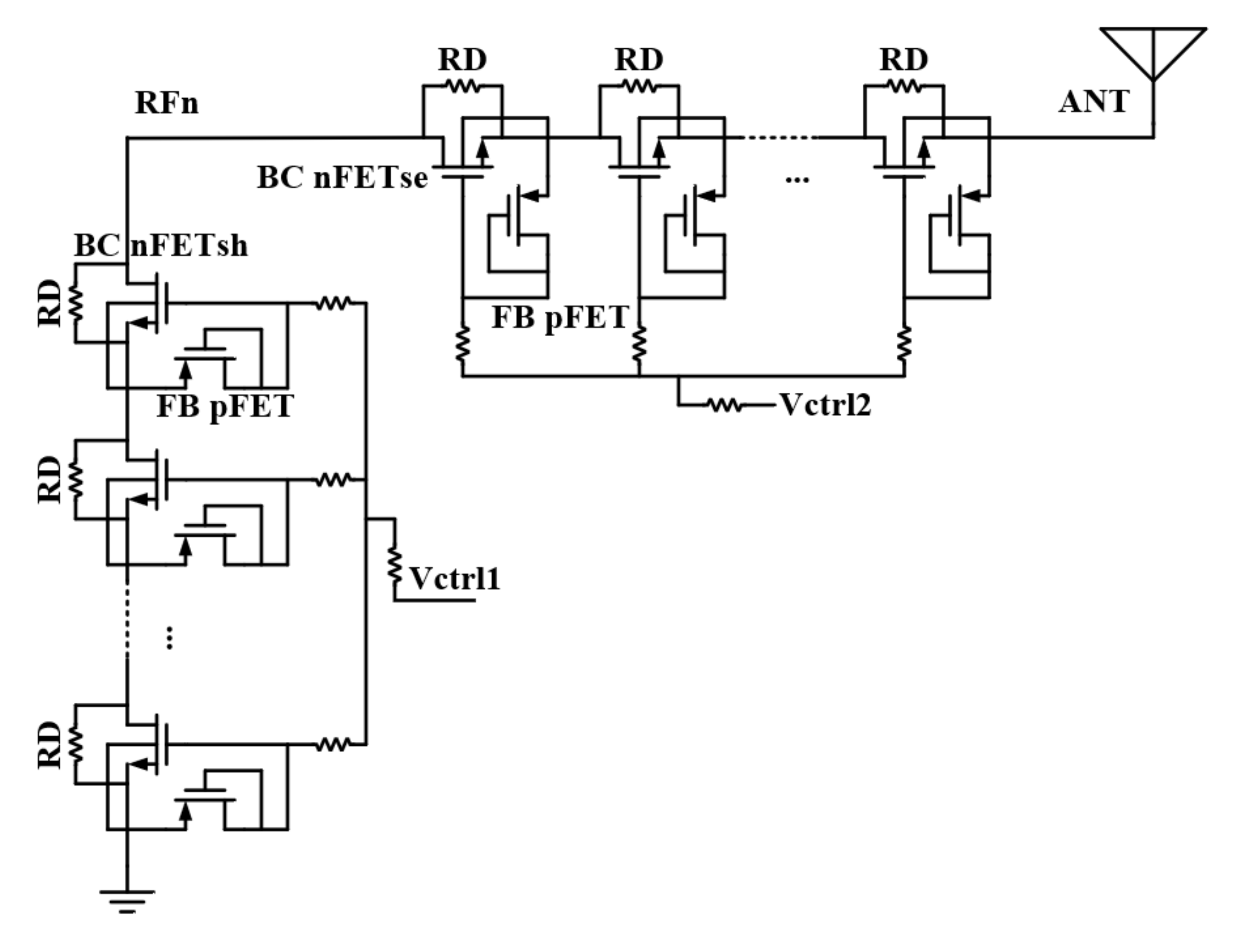
Figure 2.
The circuit of traditional CP.

Figure 3.
Timing diagram of the traditional CP.
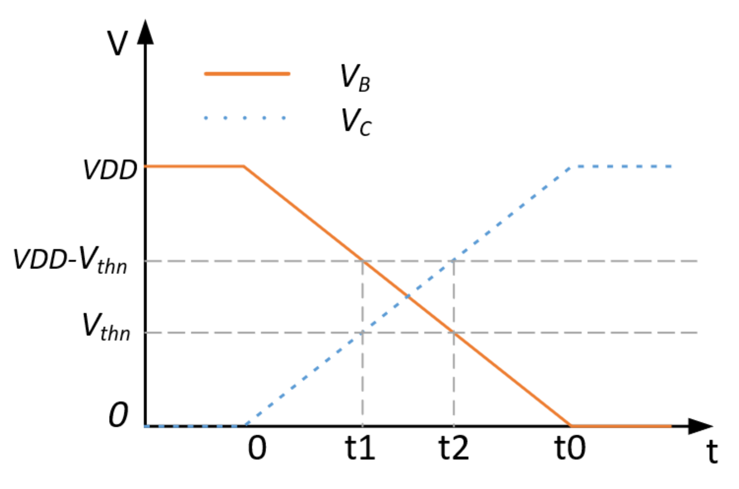
Figure 4.
Asymmetry of signals in traditional CP.

Figure 5.
Simulation results of output voltages of proposed CP and traditional CP (The frequency of oscillator is 3 MHz and the VDD is 2.4 V).
Figure 5.
Simulation results of output voltages of proposed CP and traditional CP (The frequency of oscillator is 3 MHz and the VDD is 2.4 V).

Figure 6.
The circuit of proposed CP.

Figure 7.
Timing diagram of four phase non-overlapping clocks.
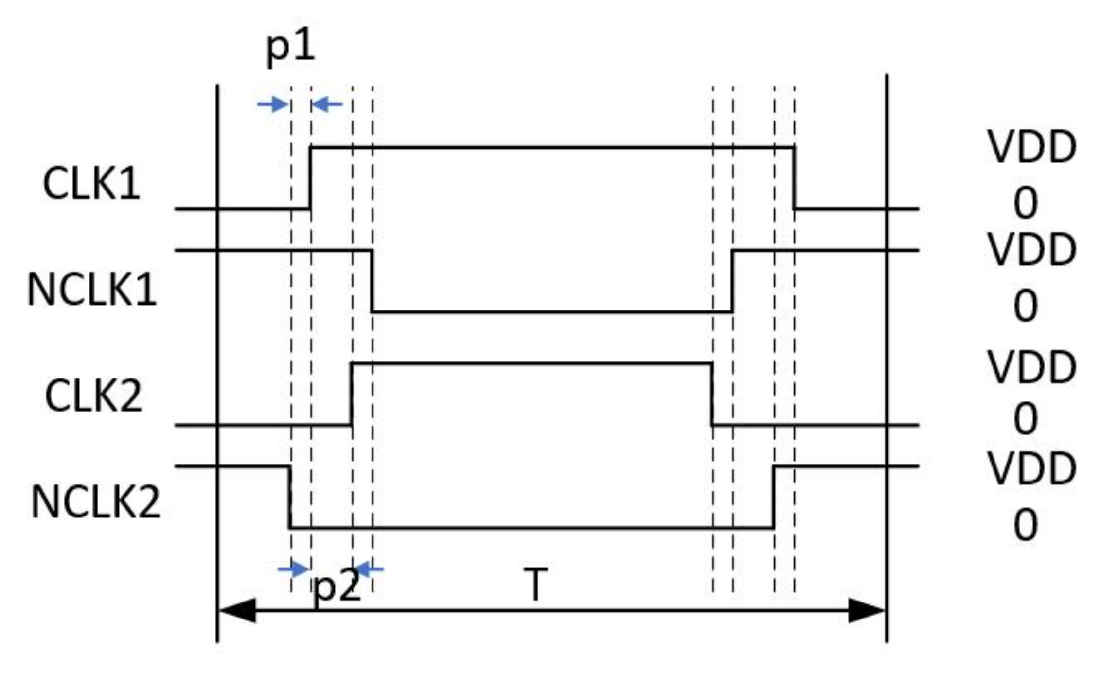
Figure 8.
Diagram of the RF switch chip.

Figure 9.
Post-layout simulation results of the output voltage with and without the proposed CP.
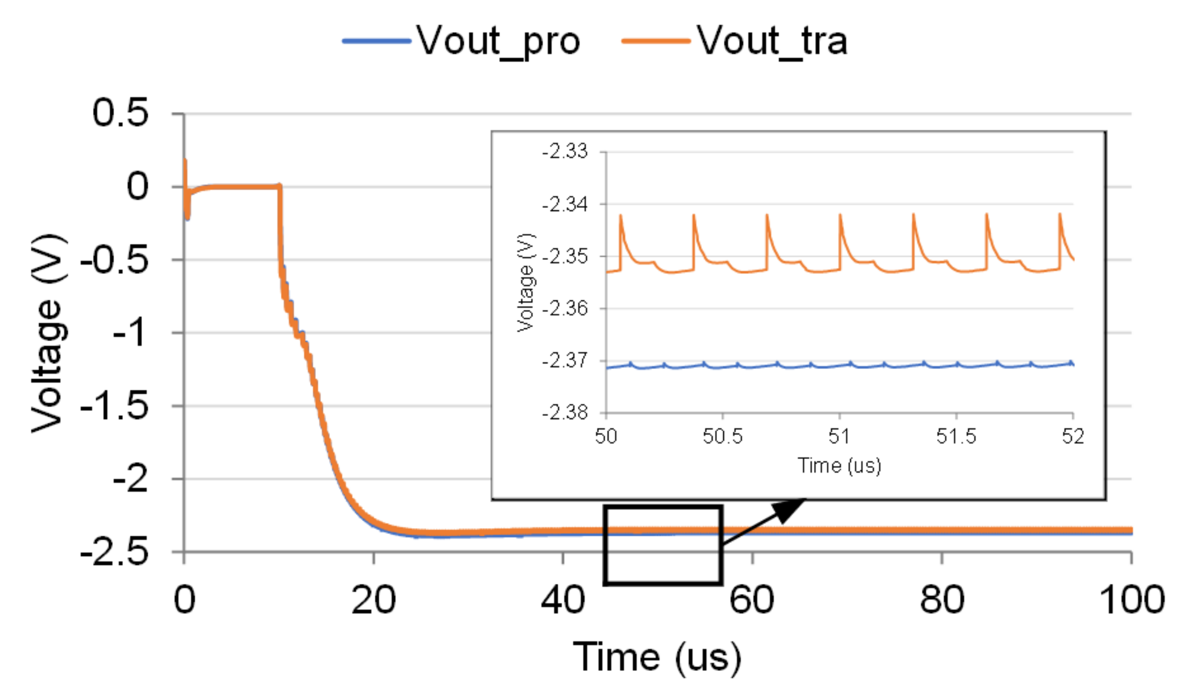
Figure 10.
Post-layout simulation results of the input and output voltages of LPF.

Figure 11.
The equivalent-circuit of RF switch.

Figure 12.
The cross section of FET.
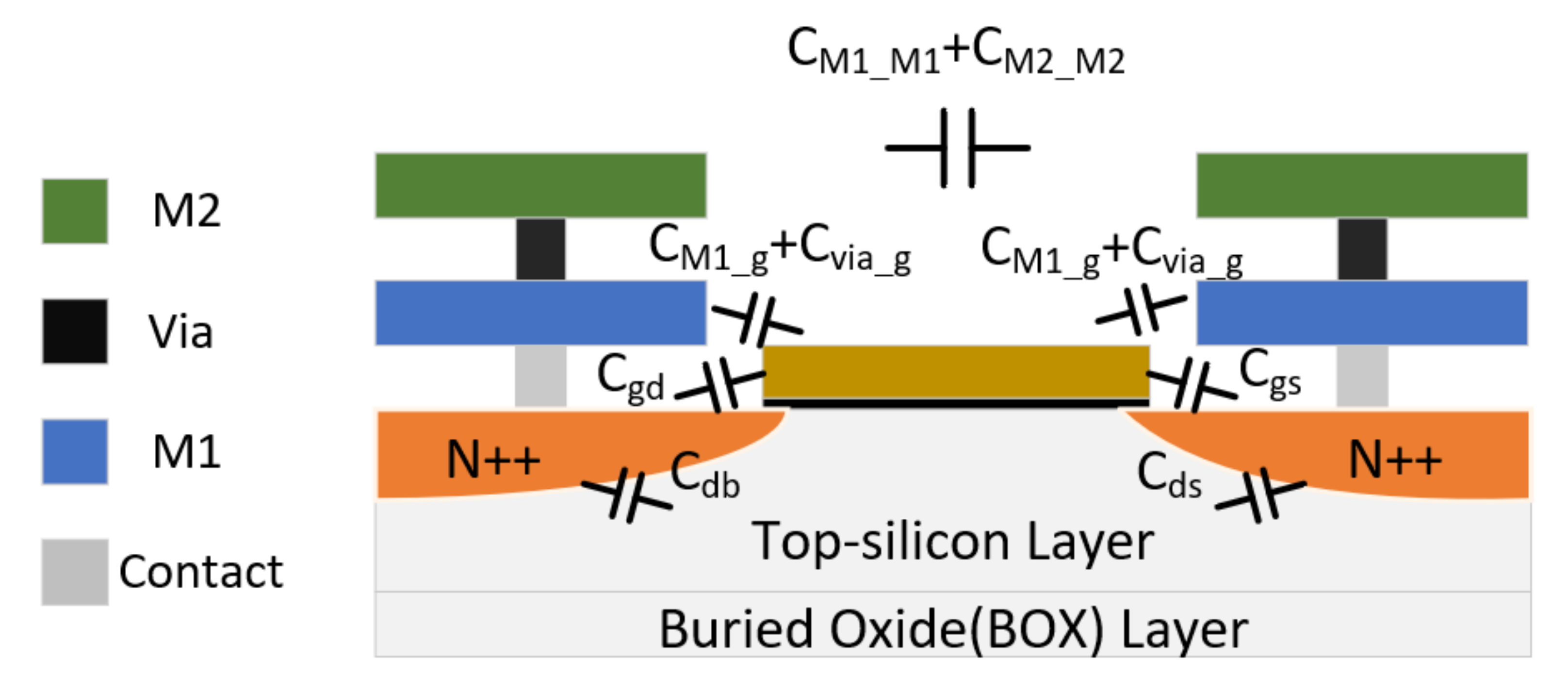
Figure 13.
The layout of: (a) Traditional switch FET; (b) FET adopted in this work.
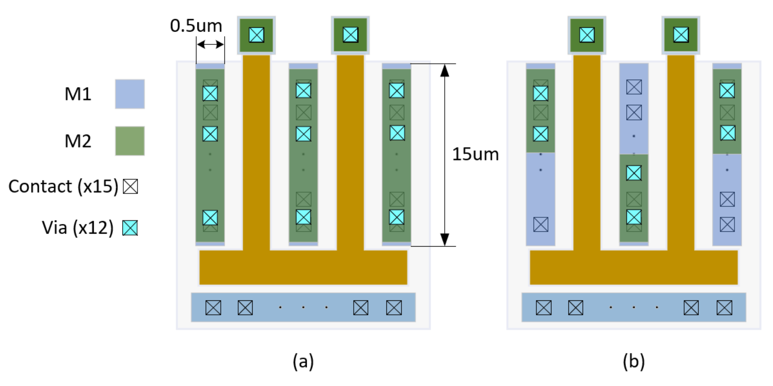
Figure 14.
Post-layout simulation results of the RF switch with and without the proposed layout.
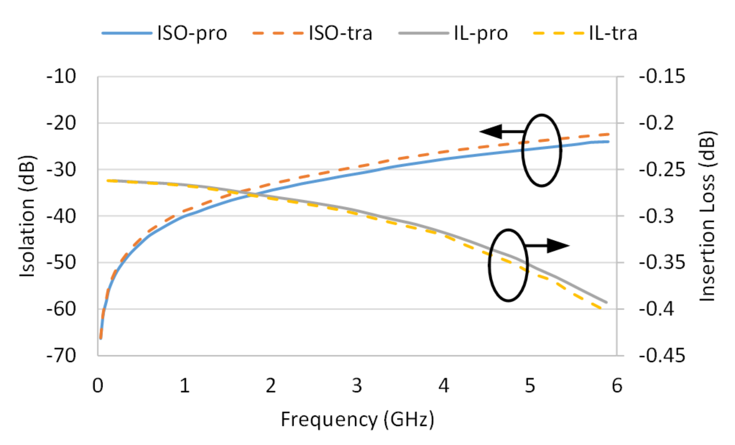
Figure 15.
Photo of the fabricated chip.
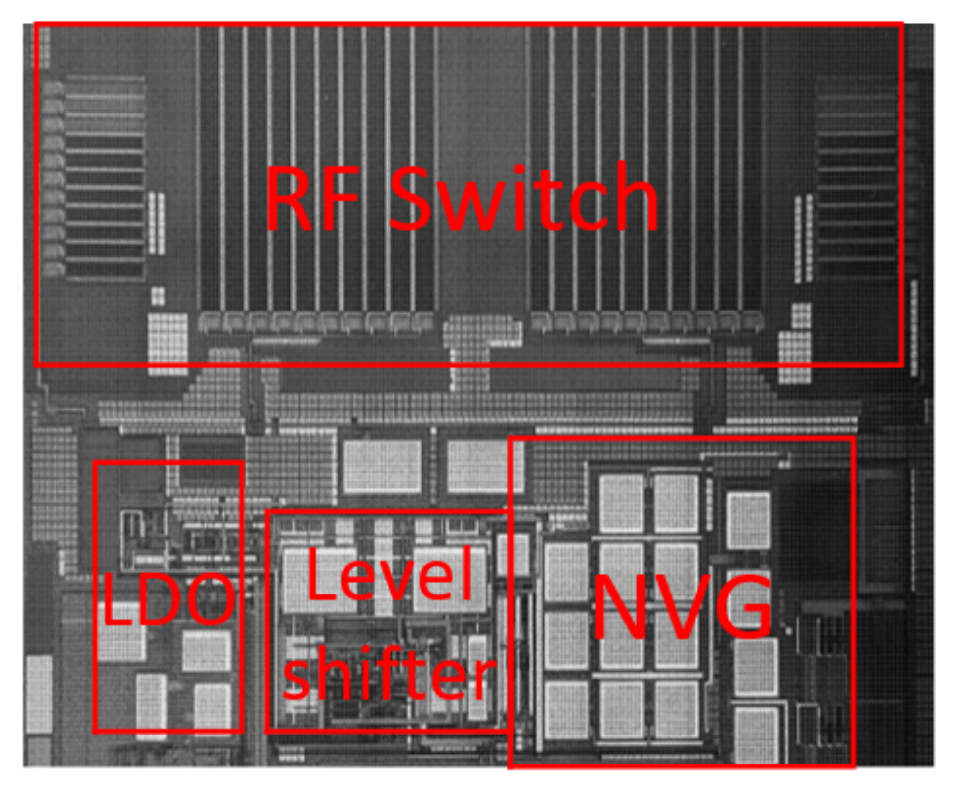
Figure 16.
Measured isolation of the SPDT switch.
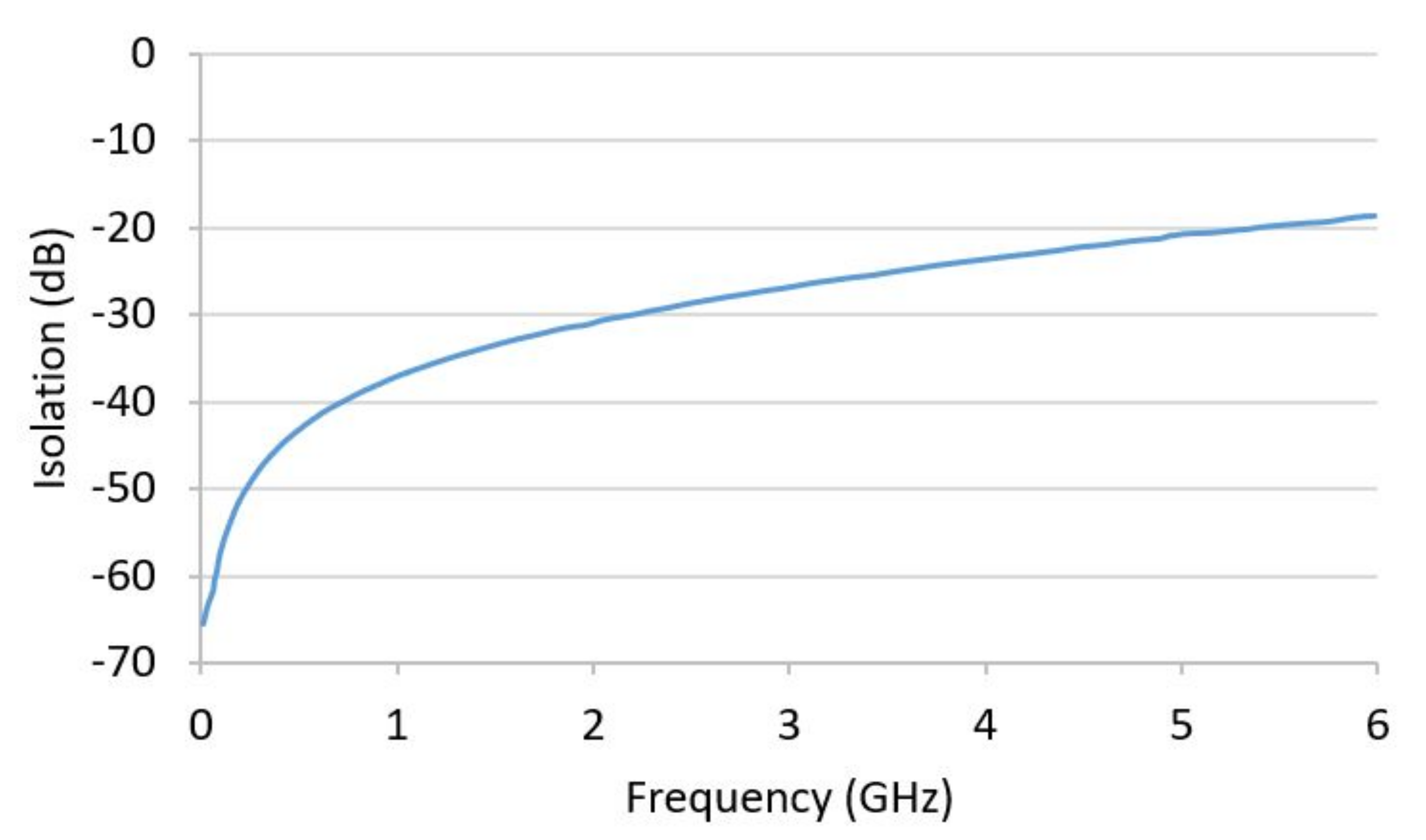
Figure 17.
Measured insertion loss of the SPDT switch.
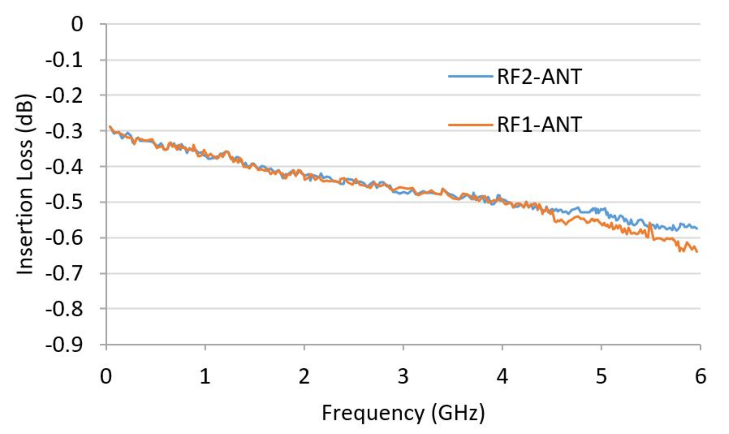
Figure 18.
Measured input power compression point of the SPDT switch.
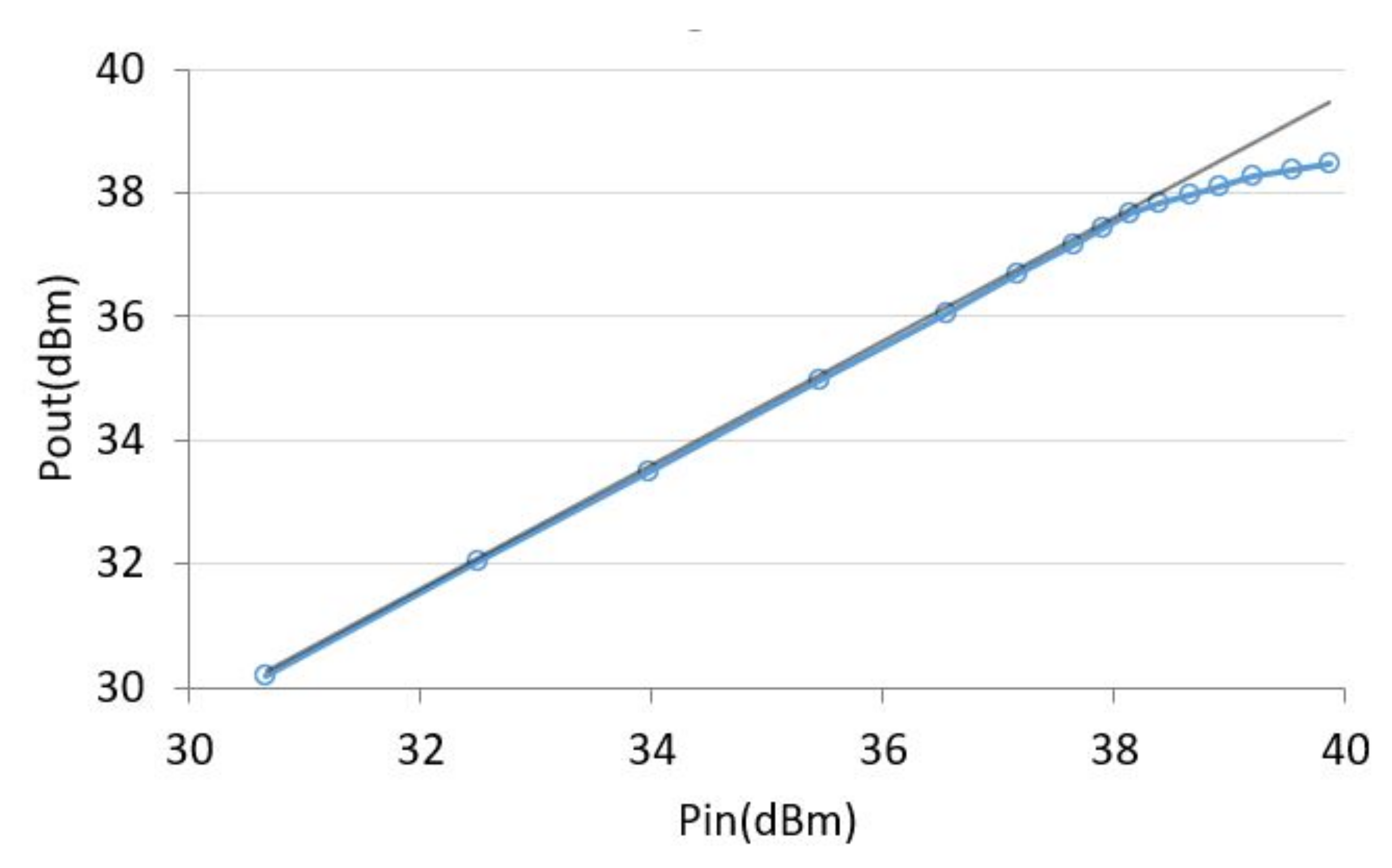
Figure 19.
Measured 3rd harmonics of the SPDT switch.


Table 1.
Performaces required in different standard.
| Wireless Standard | Peak Power (dBm) | Band (GHz) | IL (dB) | ISO (dB) | IIP3 (dBm) |
|---|---|---|---|---|---|
| GSM | 35 | 0.95/1.95 | <1 | 35 | 65 |
| 802.11x | 18 | 2.4/5.8 | <1 | 25 | 58 |
| WCDMA | 25 | 0.85/1.9/2.1 | <1 | 25 | 65 |
Table 2.
Parameters for the adopted process.
| Parameter | Value | Parameter | Value |
|---|---|---|---|
| 90.0 pF/m | (0.24 μm × 0.24 μm) | 10 | |
| 85.2 pF/m | 0.085 | ||
| 0.547 nF/m | (0.285 μm × 0.285 μm) | 3.9 | |
| 1.03 × 10 F/m | 0.080 |
Table 3.
Performance comparison with published works.
| Parameter | [10] | [6] | [30] | [31] | [5] | This Work |
|---|---|---|---|---|---|---|
| RF switch | SPDT | SP8T | SP6T | SP4T | SP4T | SPDT |
| Band (GHz) | 1/3 | 0.9/1.9 | 0.9/1.9 | DC/6 | 0.55/2.5 | DC/6 |
| IL (@1/2 GHz) | 0.7/0.9 | 0.45/0.52 | 0.82/0.88 | 0.3/0.4 | 0.55/0.75 | 0.36/0.43 |
| ISO (@1/2 GHz) | 23/27 | 46.7/22.7 | 32/28 | 38/32 | 39.4/32 | 37/31 |
| P1 dB (dBm) | 20.5 | 39.2 | 42.2 | 37.2 | 35 | 39.5 |
| Supply current (μA) | - | 50.4 | - | 80 | <1 | 37 |
| Size (mm) | 0.26 | 1.1 | 0.57 × 0.82 | - | 1.15 × 0.85 | 0.71 × 0.82 |
| Biasing technique | floating-body | negative biasing | negative biasing | negative biasing | dc-lifting | negative biasing |
| Technology | 0.18 μm CMOS | 0.18 μm SOI | 0.18 μm SOI | 0.18 μm SOI | 0.18 μm SOI | 0.18 μm SOI |
Publisher’s Note: MDPI stays neutral with regard to jurisdictional claims in published maps and institutional affiliations. |
© 2022 by the authors. Licensee MDPI, Basel, Switzerland. This article is an open access article distributed under the terms and conditions of the Creative Commons Attribution (CC BY) license (https://creativecommons.org/licenses/by/4.0/).
Share and Cite
MDPI and ACS Style
Liang, W.; Gan, Y. A High Performance 0.18 μm RF Switch for Multi-Standard. Electronics 2022, 11, 2046. https://doi.org/10.3390/electronics11132046
AMA Style
Liang W, Gan Y. A High Performance 0.18 μm RF Switch for Multi-Standard. Electronics. 2022; 11(13):2046. https://doi.org/10.3390/electronics11132046
Chicago/Turabian StyleLiang, Weishuang, and Yebing Gan. 2022. "A High Performance 0.18 μm RF Switch for Multi-Standard" Electronics 11, no. 13: 2046. https://doi.org/10.3390/electronics11132046
Note that from the first issue of 2016, this journal uses article numbers instead of page numbers. See further details here.