Communication

Study on Single Event Upsets in a 28 nm Technology Static Random Access Memory Device Based on Micro-Beam Irradiation

1
Department of Nuclear Physics, China Institute of Atomic Energy, Beijing 102413, China
2
State Key Laboratory of Intense Pulsed Radiation Simulation and Effect, Northwest Institute of Nuclear Technology, Xi’an 710024, China
3
School of Material Science and Engineering, Xiangtan University, Xiangtan 411105, China
*
Author to whom correspondence should be addressed.
Electronics 2022, 11(20), 3413; https://doi.org/10.3390/electronics11203413
Submission received: 5 September 2022 / Revised: 8 October 2022 / Accepted: 12 October 2022 / Published: 21 October 2022
(This article belongs to the Section Semiconductor Devices)

Abstract

:
As an important spaceborne electronic device, the static random access memory (SRAM) device is inevitably affected by the radiation of high-energy particles in space during its space mission. To reveal the single event effect (SEE) mechanism of 28 nm technology SRAM caused by high-energy particles, the sensitive area positioning of single event upsets (SEUs) and the distribution characteristics of multi-cell upsets (MCUs) were studied based on the pinhole heavy ion micro-beam facility. The results show that the actual range of SEUs caused by micro-beam irradiation is 4.8 μm × 7.8 μm. By moving the device platform in small steps (1 μm each step), a one-dimensional positioning method for locating the sensitive area of SEUs was established, which can reduce the dependence of localization accuracy on beam spot size, and the positioning accuracy can be improved to 1 μm. The MCU test indicates that the upset pattern is closely related to the spacing of sensitive areas within adjacent SRAM cells, and the probability of MCUs is reduced by well contacts and bit interleaving.

1. Introduction

The space radiation environment is filled with a large number of charged particles; they can cause single event effects in integrated circuit devices (such as memory devices) mounted on satellites or spacecrafts by ionization [1,2,3]. As a typical SEE, SEU can change the logic state of the integrated circuit device and even cause functional failure. In order to mitigate the radiation damage caused by SEUs, researchers use error correction codes (ECC) [4], bit interleaving [5], and memory-cell-hardening technology [6] to achieve radiation hardening of memory devices. With the scaling trends of semiconductor technology, the characteristic size of the device and the critical charge of SEUs continue to decrease, while the SEU sensitivity of the memory device is increasing. In addition to single bit upsets (SBUs), some new types of SEU also have appeared, which bring challenges to the SEE error rate prediction and radiation hardening technology [7].
Due to the high energy of heavy ions in the space environment, radial range of the ion track and charge sharing between adjacent memory cells, a single incident heavy ion may cause multi-cell upsets (MCUs) [8,9]. MCUs that occur in the same word are called multi-bit upsets (MBUs). In recent years, some radiation-hardening techniques such as ECC are mainly used to detect and correct SBUs, but these techniques cannot handle more complicated MBUs. In order to solve the problems caused by MBUs, researchers have continuously optimized the ECC technology [10].
As an important spaceborne memory device, the research on SEEs of SRAM is always the focus of domestic and international scientific research personnel, including those from national defense departments. Ground radiation tests based on the particle accelerator is an important way to study SEEs. According to size of incident beam spots, ion irradiation tests can be divided into two forms: wide-beam (centimeter scale) irradiation and micro-beam (micron scale) irradiation. The wide-beam irradiation test is mainly used to obtain macroscopic information about the radiation effect of SRAM devices, such as the curve of SEE cross section versus linear energy transfer (LET), so that the probability of SEE can be well estimated [3]. However, the SEE response obtained by wide-beam irradiation is the comprehensive effect of all irradiated regions, so the wide-beam irradiation test cannot accurately distinguish the influence of different sensitive regions on the total response. Fortunately, micro-beam irradiation can precisely position the sensitive area of SEE due to its micron-scale beam spot size. As a result, micro-beam irradiation tests often play an important role in the study of the SEE mechanism. Based on magnetic focusing or pinhole limiting, researchers have constructed a series of micro-beam facilities and carried out a lot of related research work on SEEs, which shows that micro-beam irradiation is of great importance in the SEE sensitive area positioning and SEE physical mechanism study [11,12,13].
In recent years, scientists have carried out a lot of research work on SRAM SEE by using heavy ion wide-beam irradiation tests, and obtained SRAM SEE cross sections under different LET values. In order to obtain the micro physical mechanism of SRAM SEE, there is still a lot of work to do. To understand the SEU mechanism of a new kind of 28 nm SRAM, we carried out a series of SRAM irradiation experiments based on the heavy ion micro-beam in this work. Firstly, the influence range of SEUs caused by micro-beam irradiation was evaluated. Then we obtained the distribution of SEU-sensitive areas at an improved accuracy, and the MCU/MBU characteristics are discussed respectively in the latter part.

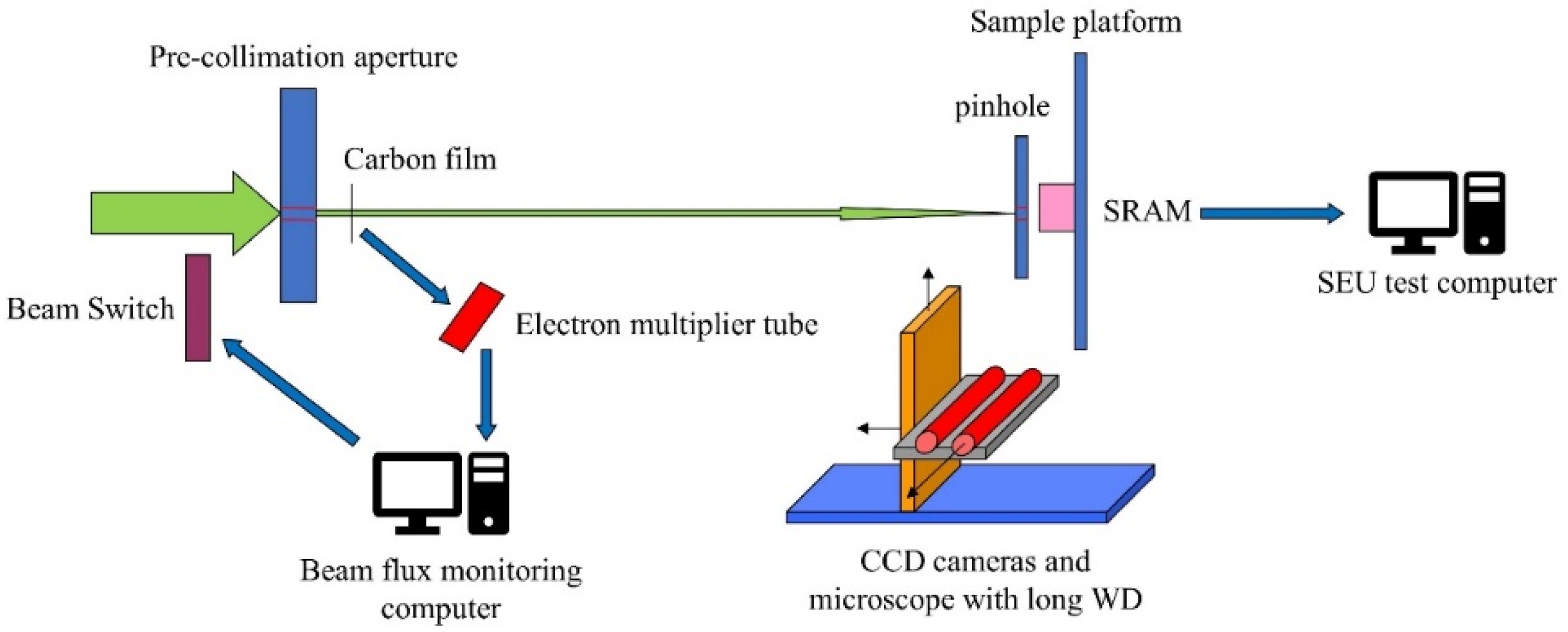
2. Experimental Setup

The experiment was carried out on the pinhole heavy ion micro-beam facility at the L30 terminal of Beijing HI-13 tandem accelerator. A self-made pinhole composed of two slits was used to limit the beam scale to the order of microns. Each slit consists of two blades and these two slits are perpendicular to each other to form a rectangular pinhole. More details about the pinhole micro-beam facility and its application could be seen in [14]. The overall experimental setup is shown in Figure 1. Each part was installed on a mobile platform and all of them were placed in the vacuum chamber except two control computers. The accelerator beam was limited by a pre-collimation apertures (millimeter scale) followed by a self-made pinhole (micron scale) to obtain the micro-beam spot. The irradiated SRAM device was observed by a long working distance (WD) microscope combined with a charge coupled device (CCD). The ion fluence can be measured indirectly by the proportional relationship with the number of secondary electrons generated by incident ions interacting with carbon film. Combined with the beam switch control system, the number of incident ions each time can be controlled to a minimum of one, which is called a single ion hit (SIH) [15].
The device under test (DUT) is a 28 nm technology 8T SRAM device with a storage of 1024 × 16 bits. The size of each memory cell is 2.17 μm × 0.52 μm. The layout of this device is shown in Figure 2 with 16 bits interleaving. This test mainly involved three areas including bit0, bit1 and bit2. The beam used in this experiment was an I ion beam with the energy of 207 MeV provided by the Beijing HI-13 tandem accelerator, with an LET of 60 MeV·cm2/mg in Si. The incident ion was perpendicular to the device’s surface, and the ion range was long enough to penetrate the surface to reach the active region. At each position, the SRAM device was irradiated by N ions. It should be noted that every ion strike should meet the conditions of SIH. After irradiation, the upset data and their logical addresses would be recorded. One of the advantages of SIH is to reduce the probability of fake MCUs as much as possible. Fake MCUs here mean that more than one ion results in several upsets at the same time due to a high fluence rate. This type of MCU is actually composed of multiple SBUs, which are not be considered in this article.

3. Results and Discussion

3.1. Evaluation of the Micro-Beam Spot Size

The micro-beam spot size is an important geometric parameter that has a great impact on the performance of the pinhole micro-beam facility. However, the range of SRAM upsets caused by the ion beam passing through the pinhole also needs to be considered and even has more experimental significance, as it represents the actual influence range of the micro-beam on the SRAM device. Therefore, in this article, we determined the micro-beam spot size by the range of SEUs caused by micro-beam irradiation.
Bit1 area was irradiated and the number of incident ions N was 100. According to the known conversion relationship between logical addresses and physical addresses, the two-dimensional distribution of all upset cells was drawn in Figure 3. The cell arrangement of every bit area is 64 columns × 16 rows, a total of 1024 cells. Since the aspect ratio of each cell is about 1:4 (0.52:2.17 precisely), each bit area is approximately a square. The upset counts were projected to the X and Y directions respectively, and NX and NY were then obtained by the accumulation of upset counts. The results are shown in Figure 4. The distances along X and Y direction corresponding to 10–90% of the total upset counts are defined as the width and height of the beam spot respectively, which is shown as 4.8 μm × 7.8 μm. The linear interpolation at adjacent two points in Figure 4 was used to get numerical values. This result is marked with a red solid frame in Figure 3. The number of ions included in this part accounts for 86% of the total. The red dashed frame in Figure 3 represents the most conservative estimate of the beam spot size including all upsets, with a size of 10.9 μm × 15.2 μm.
For the ions in the region between the solid frame and the dashed frame, due to the pinhole structure consisting of two vertical slits, if the inner edge of the slit is slightly uneven or not completely perpendicular to the beam direction, some incident ions will be scattered to the outer area. For the ions within the solid frame, MCUs have an obvious impact. In this experiment, the average ratio of MCUs is about 10% (more details in Section 3.3) and most of them are distributed inside the solid frame. As found in other works [4], MCUs could affect more than two (usually up to ten) cells in nanotechnology SRAMs at one time, which is consistent with Figure 3. Meanwhile, the insufficient stability of the device platform will lead to slight a mechanical vibration. This micron-scale vibration may have an effect on the whole region.

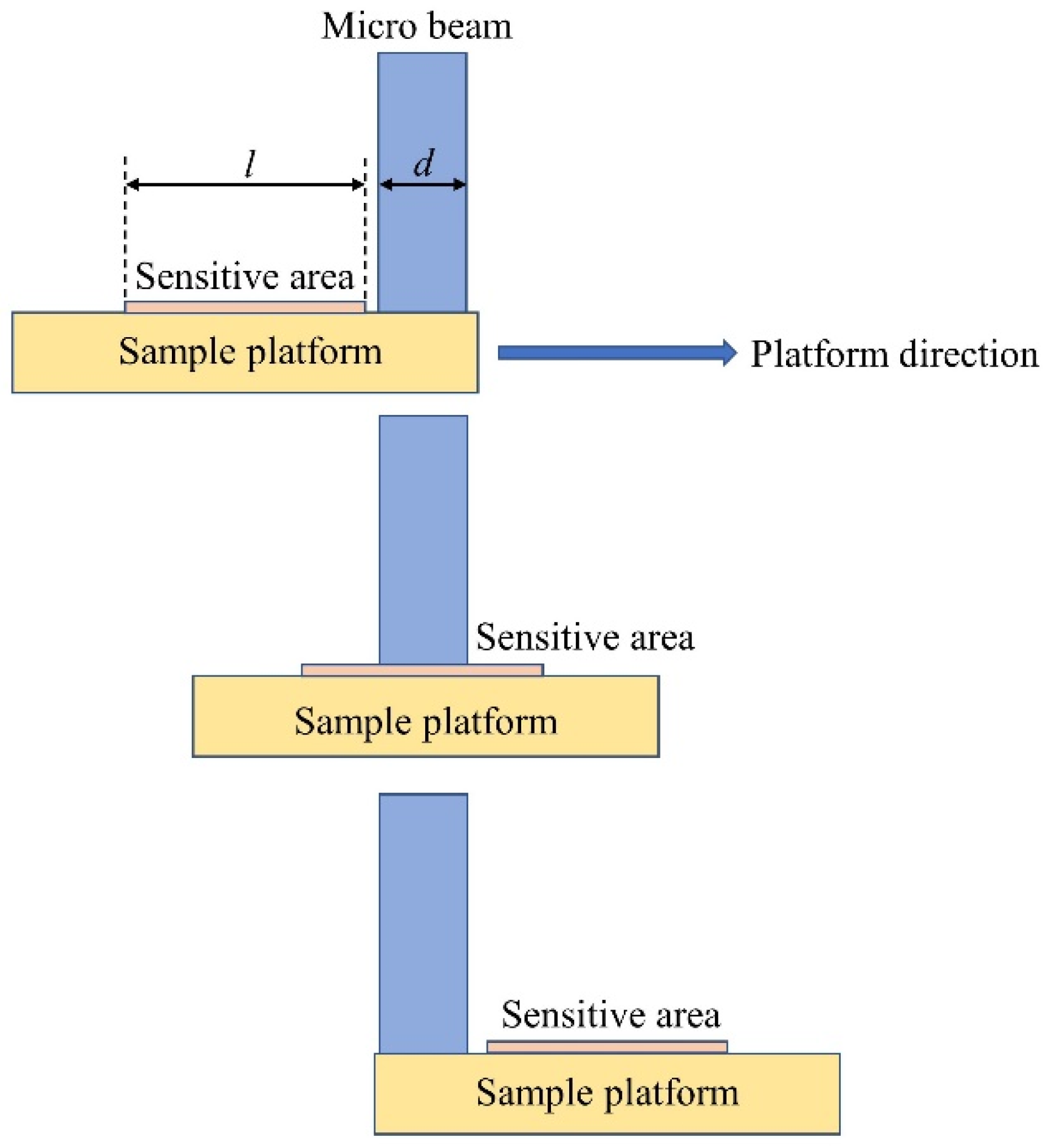
3.2. One-Dimensional SEU Sensitive Area Positioning

The position information of the upset cells can be obtained by the micro-beam, so the SEU sensitive area of the SRAM device can be located. In this section, we did not try to acquire the distribution of sensitive areas inside one single cell. Instead, our aim was to locate the whole bit1 sensitive area, especially the boundary. The accuracy of the positioning system is usually represented by the beam spot size [11], and this size is often subject to pinhole manufacturing processes or magnetic focusing ability. So, a novel SEU-sensitive-area positioning method was proposed and verified.
The SRAM device moved from left to right horizontally at a given step length as shown in Figure 5. The numbers of incident ions and upsets occurring at each position were N and N′. The step length was set to be 1 μm. The horizontal width of the beam spot and the sensitive area were defined as d and l, respectively.
Figure 6 shows the upset results of the bit1-sensitive area, and other sensitive areas are quite similar. The Y-axis in the figure represents N′/N rather than N′ for the reason of normalization. The transition at the boundary is quite sharp, which indicates a high positioning accuracy. The widths of the slope part and horizontal part in Figure 6 equal d and ld according to the geometric relationship. The least square method was used to perform linear fitting of these two parts, and the fitting result is that d = 10.1 μm, l = 39.3 μm. According to the results in Section 3.1, the estimate of the spot width considering all the upsets is approximately 10 μm, which was very close to the value of d. At the same time, according to the designed SRAM layout dimensions, the actual horizontal width of bit1 sensitive area including all the cells and spacings is 39 μm. So, the value of l can give a good estimate of the actual size of the sensitive area and the error is less than 1 μm.
These results show the feasibility of the SEU-sensitive-area positioning method with a small step movement of the device platform. In the case of one-dimensional movement, when irradiating the SRAM device with a 10 μm-wide beam spot, the accuracy of this positioning method reaches 1 μm, which is obviously improved. For the heavy ion beam required in SEE study, the magnetic focusing micro-beam needs a strong focusing ability to achieve the heavy ion beam to 1 μm at a high construction cost. Meanwhile, the pinhole micro-beam is often limited by the fineness of the pinhole manufacturing process, which makes it difficult to achieve a 1 μm or smaller size. However, there is much room to improve the positioning accuracy of mobile platforms. Although the study on this method is still in the preliminary stage, it can greatly weaken the dependence of positioning accuracy on the micro-beam spot size and provide more redundancy for micro-beam technology. This method could achieve higher or even nano-scale accuracy by applying the displacement platform with a higher accuracy and smaller step length, and then it could be used to locate sensitive areas inside one cell of nanotechnology devices in future studies.

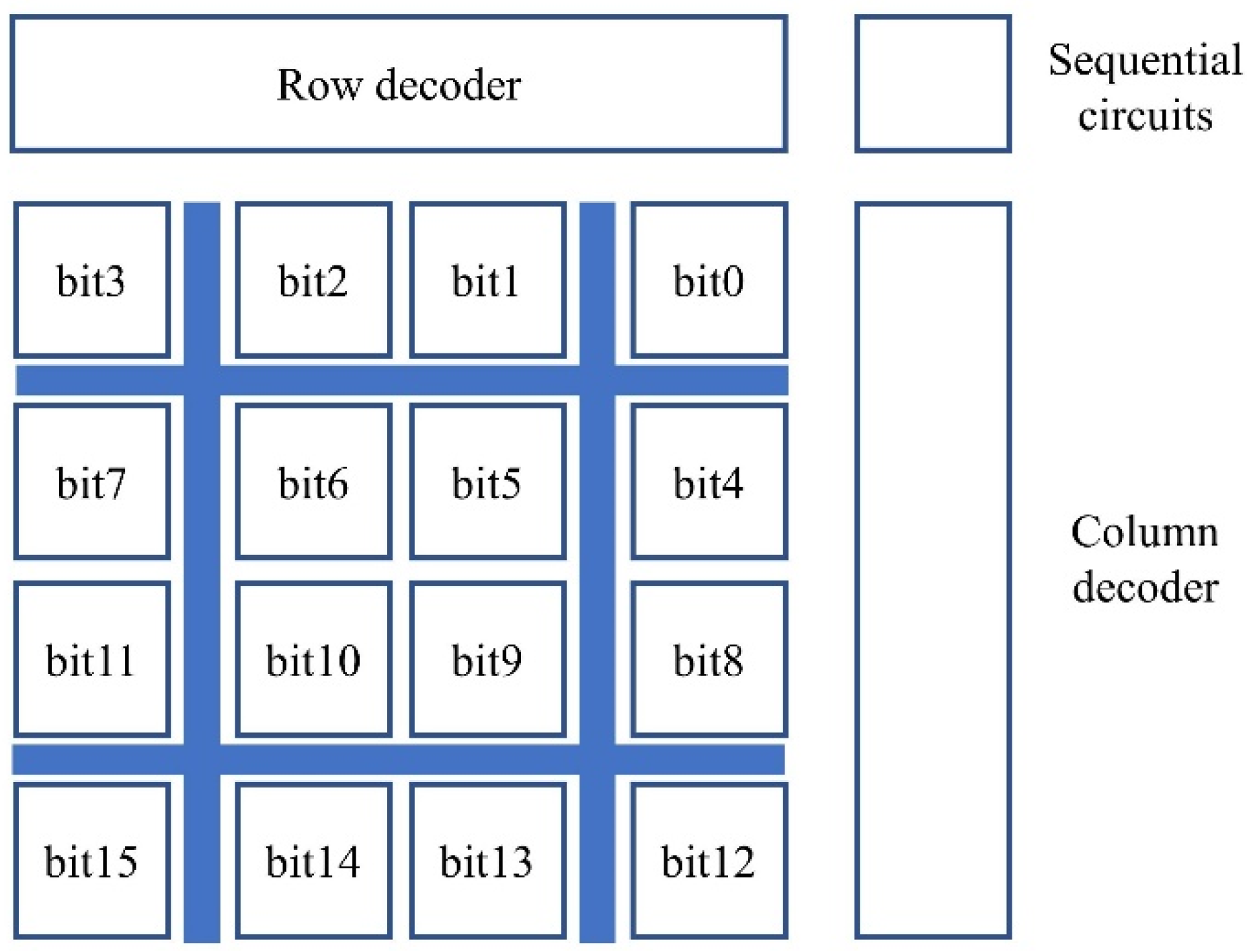
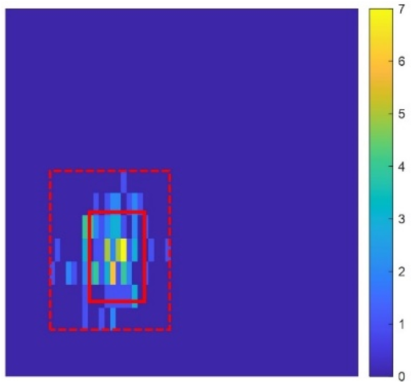
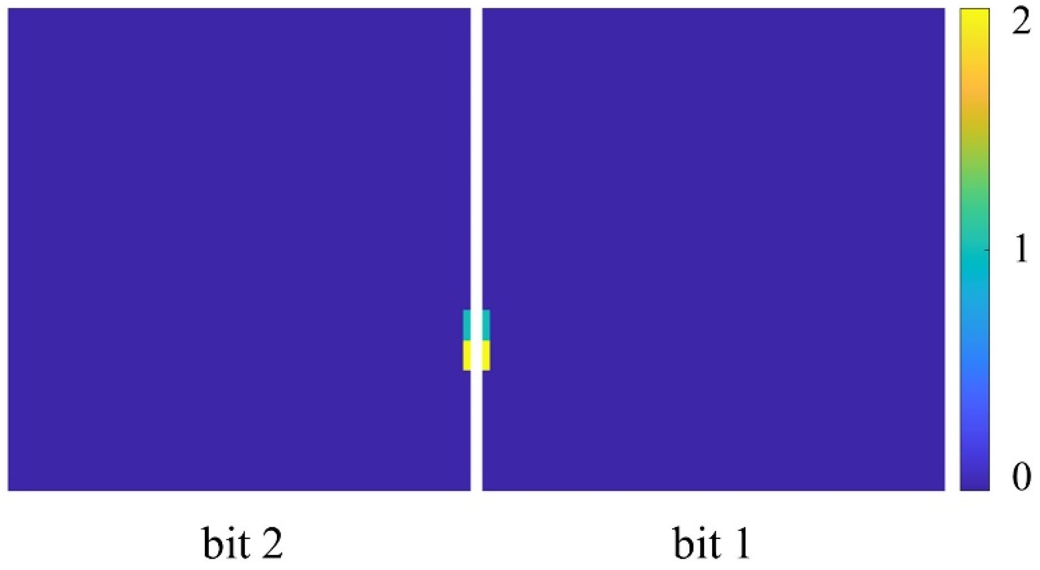
3.3. MCU/MBU Characteristics

In Figure 6, NN > 1 in the central area indicates that a single incident ion causes more than one cell to upset, which means there is a certain proportion of MCUs. The distribution of multiplicity M is shown in Figure 7. Most of the MCUs are two-bit MCUs while the maximum of M is seven. This is a common result in most MCU works [4,9,10]. There are also some studies that analyze different patterns of MCUs [9,10], but few of them explain the probability difference of these MCU patterns, especially for the most common two-bit MCUs.
The ratio of two-bit MCUs with different upset patterns are shown in Table 1. The probability of pattern (a) is largest both in our work and refs [9,10]. However, the probability of pattern (b) is larger than (c) in ref [9], while it is the opposite in ref [10]. Our result is consistent with ref [10]. Here, we provide a possible explanation that the different probabilities of these three patterns are due to the geometric distribution of the sensitive area within adjacent cells as shown in Figure 8. The scale of geometric dimensions in Figure 8 is consistent with the real layout for comparison. The drain areas of MOSFETs in OFF state are sensitive, which are marked as blue dots in the figure. The spacings a, b and c correspond to the MCU patterns (a), (b) and (c) respectively. It is obvious that the smaller the spacing, the greater the probability of MCUs.
Every two cell rows are separated by a well contact band and the well contact could hinder charge sharing between two adjacent cells in the vertical direction. At the same time, the well contact can quickly drain the excess carriers caused by incident ions and effectively reduce the influence of well potential disturbance [16]. Therefore, the two cells in the vertical direction are less prone to upset, which means that the probability of patterns (b) and (c) is much lower than that of pattern (a). Moreover, according to Figure 8, b (=a) > c, so the probability of pattern (c) is higher than that of pattern (b).
Finally, the MBU characteristics are discussed. Because the bit interleaving layout was used in the irradiated SRAM device and 16 bits in the same word are distributed in 16 separate regions, MBUs occur only when ions strike between two adjacent bits resulting in upset cells at the same time. The SRAM device was irradiated from right to left and there are five areas involved: bit0, bit1, bit2, the area between bit0 and bit1, and the area between bit1 and bit2. There are three MBUs occurring during the experiment, that is, 0xFFF9 once and 0x0006 twice. The corresponding binaries are 1111 1111 1111 1001 and 0000 0000 0000 0110 respectively, which means all of them are the type of MBUs where bit1 and bit2 upsets, either 1 → 0 or 0 → 1. The physical address distribution of the three MBUs is shown in Figure 9.
The physical addresses of adjacent bits are mirror symmetrical arranged, so the upset cells of MBUs in Figure 9 are mirror symmetrical too. The spacing between bit0 and bit1 is 8.5 μm, while the spacing between bit1 and bit2 is only 0.7 μm. Therefore, the probability of the latter type of MBUs is much higher. When ions strike the region between bit1 and bit2, due to the radial distribution of ion energy and charge diffusion, the adjacent symmetrical two cells may upset at the same time.

4. Conclusions

To better understand the physical mechanism of SRAM SEE, we have established a one-dimensional SEU sensitive area positioning method that can improve the micro-beam positioning accuracy significantly. Through this method, the horizontal width of bit1 area was measured and compared with the layout information, which shows good consistency. The patterns of two-bit MCUs were also classified and discussed, indicating that the well contact could reduce the probability of adjacent cell upsets in the vertical direction, and the spacing of sensitive areas has a great influence on the probability of MCUs with different patterns. Because the physical addresses of adjacent bits in the same word are mirror symmetrical, there is still a certain probability of MBUs when the beam irradiates the areas between two adjacent bits with small spacing.

Author Contributions

Conceptualization, H.S., R.S. and G.G.; methodology, H.S.; software, H.S., W.Z., F.Z. and J.L.; validation, H.S.; investigation, H.S., Y.C. and Y.Z.; resources, G.G.; data curation, H.S., W.Z. and R.S.; writing—original draft preparation, H.S.; writing—review and editing, G.G., Z.Z. and W.Z.; supervision, G.G.; project administration, G.G.; funding acquisition, G.G. All authors have read and agreed to the published version of the manuscript.

Funding

This research received no external funding.

Data Availability Statement

The data used to support the findings of this study are available from the corresponding author upon request.

Conflicts of Interest

The authors declare no conflict of interest.

References

  1. Fleetwood, D.M. Radiation effects in a post-Moore world. IEEE Trans. Nucl. Sci. 2021, 68, 509–545. [Google Scholar] [CrossRef]
  2. Kobayashi, D. Scaling trends of digital single-event effects: A survey of SEU and SET parameters and comparison with transistor performance. IEEE Trans. Nucl. Sci. 2020, 68, 124–148. [Google Scholar] [CrossRef]
  3. Dodd, P.; Massengill, L. Basic mechanisms and modeling of single-event upset in digital microelectronics. IEEE Trans. Nucl. Sci. 2003, 50, 583–602. [Google Scholar] [CrossRef]
  4. Saiz-Adalid, L.-J.; Reviriego, P.; Gil, P.; Pontarelli, S.; Maestro, J.A. MCU Tolerance in SRAMs through Low-Redundancy Triple Adjacent Error Correction. IEEE Trans. Very Large Scale Integr. (VLSI) Syst. 2014, 23, 2332–2336. [Google Scholar] [CrossRef] [Green Version]
  5. Baeg, S.; Wen, S.; Wong, R. SRAM Interleaving Distance Selection With a Soft Error Failure Model. IEEE Trans. Nucl. Sci. 2009, 56, 2111–2118. [Google Scholar] [CrossRef]
  6. Qi, C.; Xiao, L.; Wang, T.; Li, J.; Li, L. A Highly Reliable Memory Cell Design Combined with Layout-Level Approach to Tolerant Single-Event Upsets. IEEE Trans. Device Mater. Reliab. 2016, 16, 388–395. [Google Scholar] [CrossRef]
  7. Dodd, P.E.; Shaneyfelt, M.R.; Schwank, J.R.; Felix, J.A. Current and future challenges in radiation effects on CMOS electronics. IEEE Trans. Nucl. Sci. 2010, 57, 1747–1763. [Google Scholar] [CrossRef]
  8. Liu, J.; Yan, S.; Xue, J.; Wang, Y. Comparison of ionization track structure models for electronic devices of different sizes. Nucl. Instrum. Methods Phys. Res. Sect. B 2019, 444, 43–49. [Google Scholar] [CrossRef]
  9. Radaelli, D.; Puchner, H.; Wong, S.; Daniel, S. Investigation of multi-bit upsets in a 150 nm technology SRAM device. IEEE Trans. Nucl. Sci. 2005, 52, 2433–2437. [Google Scholar] [CrossRef]
  10. Wirthlin, M.; Lee, D.; Swift, G.; Quinn, H. A Method and Case Study on Identifying Physically Adjacent Multiple-Cell Upsets Using 28-nm, Interleaved and SECDED-Protected Arrays. IEEE Trans. Nucl. Sci. 2014, 61, 3080–3087. [Google Scholar] [CrossRef]
  11. Horn, K.; Doyle, B.; Sexton, F. Nuclear microprobe imaging of single-event upsets. IEEE Trans. Nucl. Sci. 1992, 39, 7–12. [Google Scholar] [CrossRef]
  12. Horn, K.; Doyle, B.; Sexton, F.; Laird, J.; Saint, A.; Cholewa, M.; Legge, G. Ion beam induced charge collection (IBICC) microscopy of ICs: Relation to single event upsets (SEU). Nucl. Instrum. Methods Phys. Res. Sect. B 1993, 77, 355–361. [Google Scholar] [CrossRef]
  13. Schone, H.; Walsh, D.; Sexton, F.; Doyle, B.; Dodd, P.; Aurand, J.; Flores, R.; Wing, N. Time-resolved ion beam induced charge collection (TRIBICC) in micro-electronics. IEEE Trans. Nucl. Sci. 1998, 45, 2544–2549. [Google Scholar] [CrossRef] [Green Version]
  14. Yang, W.; Du, X.; He, C.; Shi, S.; Cai, L.; Hui, N.; Guo, G.; Huang, C. Microbeam heavy-ion single-event effect on Xilinx 28-nm system on chip. IEEE Trans. Nucl. Sci. 2018, 65, 545–549. [Google Scholar] [CrossRef]
  15. Fischer, B.; Heiß, M.; Cholewa, M. About the art to shoot with single ions. Nucl. Instrum. Methods Phys. Res. Sect. B 2003, 210, 285–291. [Google Scholar] [CrossRef]
  16. Zhangd, K.; Furuta, J.; Kobayashi, K.; Onodera, H.; Zhang, K. Dependence of Cell Distance and Well-Contact Density on MCU Rates by Device Simulations and Neutron Experiments in a 65-nm Bulk Process. IEEE Trans. Nucl. Sci. 2014, 61, 1583–1589. [Google Scholar] [CrossRef]
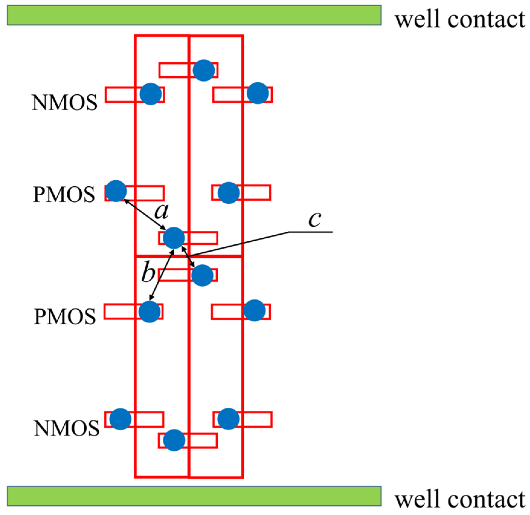
Figure 1. Schematic of the SEU experimental setup (The green arrow represents the ion beam direction).
Electronics 11 03413 g001
Figure 2. Schematic of the SRAM device layout.
Electronics 11 03413 g002
Figure 3. Two-dimensional distribution of upset cells (upset counts are consistent with the color bar in the right).
Electronics 11 03413 g003
Figure 4. Plot of upset counts in the X (a) and Y (b) projection from two-dimensional distribution.
Electronics 11 03413 g004
Figure 5. Schematic of SEU-sensitive-area positioning method.
Electronics 11 03413 g005
Figure 6. Plot of normalized upset counts in the horizontal direction.
Electronics 11 03413 g006
Figure 7. Distribution of multiplicity M.
Electronics 11 03413 g007
Figure 8. Schematic of sensitive areas (blue dots) within four adjacent cells.
Electronics 11 03413 g008
Figure 9. Two-dimensional distribution of three MBUs.
Electronics 11 03413 g009
Table 1. Ratios of different patterns of two-bit MCUs.
(a)(b)(c)
PatternsElectronics 11 03413 i001Electronics 11 03413 i002Electronics 11 03413 i003, Electronics 11 03413 i004
Percentage56%17%27%
Publisher’s Note: MDPI stays neutral with regard to jurisdictional claims in published maps and institutional affiliations.

