Article

Electrical Characterization of Through-Silicon-via-Based Coaxial Line for High-Frequency 3D Integration (Invited Paper)

1
School of Integrated Circuits and Electronics, Beijing Institute of Technology, Beijing 100081, China
2
Tangshan Research Institute of BIT, Tangshan 063000, China
3
Engineering Department, University of Messina, 98166 Messina, Italy
4
BIOMORF Department, University of Messina, 98125 Messina, Italy
*
Author to whom correspondence should be addressed.
Electronics 2022, 11(20), 3417; https://doi.org/10.3390/electronics11203417
Submission received: 6 October 2022 / Revised: 18 October 2022 / Accepted: 19 October 2022 / Published: 21 October 2022
(This article belongs to the Special Issue Advanced RF, Microwave Engineering, and High-Power Microwave Sources)

Abstract

:
Through-silicon-via (TSV)-based coaxial line techniques can reduce the high-frequency loss due to the low resistivity in the silicon substrate and thus can improve the efficiency of vertical signal transmission. Moreover, a TSV-based coaxial structure allows easily realizing the impedance matching in RF/microwave systems for excellent electrical performance. However, due to the limitations of existing available dielectric materials and the difficulties and challenges in the manufacturing process, ideal coaxial TSVs are not easy to obtain, and thus, the achieved electrical performance might be unexpected. In order to increase the flexibility of designing and manufacturing TSV-based coaxial structures and to better evaluate the fabricated devices, modeling and analysis theories of the corresponding high-frequency electrical performance are proposed in the paper. The theories are finally well validated using the finite-element simulation results, hereby providing guiding rules for selecting materials and improving manufacturing techniques in the practical process, so as to optimize the high-frequency performance of the TSV structures.

1. Introduction

Through-silicon-via (TSV) technology [1,2,3] is one of the most attractive three- dimensional (3D) integration methods for high-speed and high-performance applications. It has the capability of electrically connecting and communicating densely-packed devices with different functionalities [3,4], such as integrated circuits and RF/microwave modules. Particularly, it can vertically integrate analog circuits, digital circuits, MEMS devices, etc., for efficient heterogeneous systems [5,6,7,8]. With the fast development of TSV-based 3D heterogeneous integrated systems, novel high-frequency vertical connectivity and communication techniques are increasingly required. For instance, TSV structures with good high-frequency performance should be designed for a microwave-device integrated 3D system.
Coaxial transmission line is a typical and widely used high-frequency structure for electromagnetic field transmission, due to its advantage of being able to efficiently transmit transverse electromagnetic waves and having low loss. Therefore, coaxial shield TSVs have been designed for high-speed signal transmission [9] and used as an efficient vertical transition in flip-chip structures [10]. The basic configuration of a coaxial shield TSV has a central signal conductor surrounded by an outside concentric ground shell, which can consequently suppress undesirable substrate crosstalk [11] and effectively reduce the losses caused by radiation and coupling when it is used for transmitting microwave signals [12,13]. It has been validated that compared to the common signal-ground (S-G) paired TSVs, such type of coaxial TSVs can offer better signal integrity and show better electrical performance at high frequencies [7]. In addition, the coaxial-TSV technique has the flexibility in impedance controlling for the impedance matching of RF/microwave systems, to achieve excellent RF performance [14]. For instance, a multi-layer or fan-shaped dielectric can be used to replace the typical single homogeneous dielectric between the inner and outer conductors [15], to improve the design flexibility of the coaxial-TSV impedance.
Based on the TSV fabrication process, slightly different coaxial-TSV fabrication techniques are developed [11,14,16]. Generally, the fabrication starts by etching deep via holes in the silicon substrate by wet or dry methods, including the laser drilling approach or the deep reactive ion etching (DRIE) method [17]. Then, the Cu ground wall of the coaxial TSV is formed by using the plating technique [9] or the sputtering method. Silicon oxide and nitride might be required to be deposited in advance to line the vias, and, in order to increase the adhesion to dielectrics, a thin layer of Ti is often deposited prior to Cu, to act as an adhesion layer. Next, the dielectric deposition is performed along the sidewall of the vias, which is followed by the electroplating of Cu to fill the vias, forming a cylindrical signal conductor. Studies on the fabrication difficulties, the dielectric properties, the physical and chemical properties of available manufacturing materials, the desired electrical performance, etc., are carried out to obtain high-performance coaxial TSVs in the manufacturing process [8]. For instance, SU-8 is preferably considered when a thick dielectric is required [11], due to its high aspect ratio feature [18,19]. Considering that fabricating the cylindrical TSVs is a more simple procedure; a ring of cylindrical TSVs are designed to replace the annular coaxial TSV, forming a coaxial-like TSV [20,21]. Additionally, silicon-core coaxial TSVs are proposed and studied [22], to reduce the processing time for fully filling the inner and outer conductors with metal [23,24].
Although more and more TSV processing materials and technologies have been considered in designing and manufacturing the high-frequency coaxial TSVs or coaxial-like TSVs, theories on improving and optimizing the electrical performance of these structures are still required to help with selecting appropriate TSV structures, materials, and fabrication procedures for different 3D integration applications. Moreover, the electrical performance can be dramatically affected by the fabrication process. For instance, since there is a fabrication tolerance in the Si-etching and Cu-filling process, there might be a center offset of the inner conductor in the coaxial TSV [11,16,20]. The off-centered coaxial TSV might consequently provide a different electrical performance from the designed one. Further, voids are easily formed when filling the high aspect ratio (AR) TSV, and thus, dimensions of the designs should be optimized according to the realistic fabrication conditions.
Here, an approach is presented for modeling and analyzing a TSV-based coaxial structure. It investigates the impacts of coaxial-TSV materials and geometries on their electrical performance up to 40 GHz, providing some design theories and rules. A theory related to the coaxial-like TSV is further derived, providing some guiding suggestions for the practical manufacturing process. The characteristic impedance of these TSV-based coaxial lines is mainly studied using the conformal mapping method [25,26,27,28] and validated using the finite element method (FEM) simulations, which provide an accurate description of the considered microwave structure [28,29,30,31].

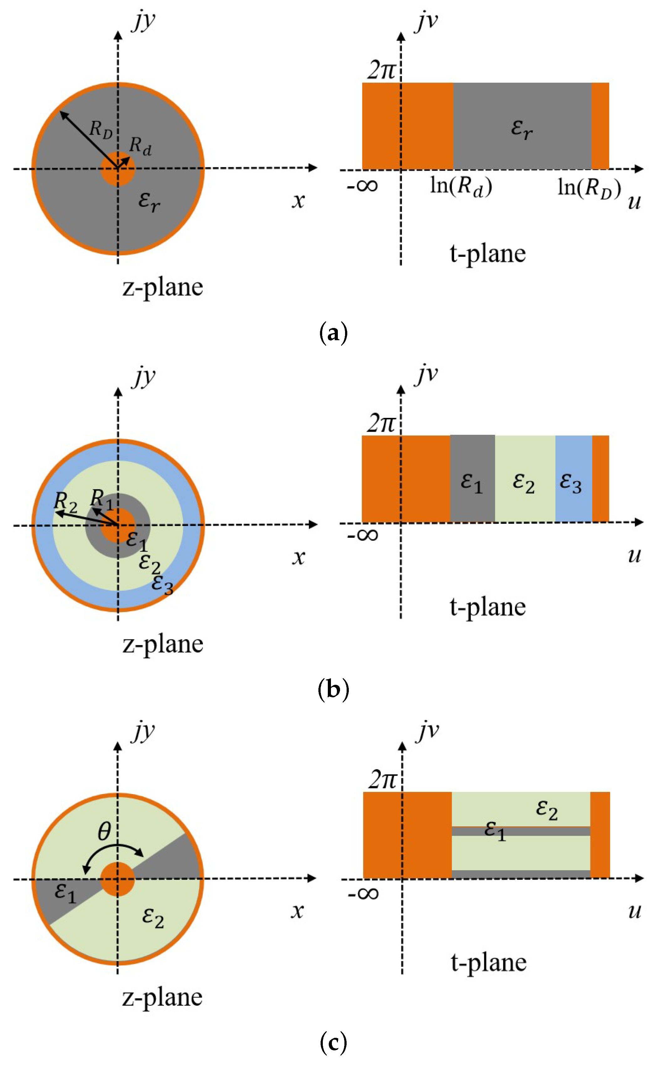
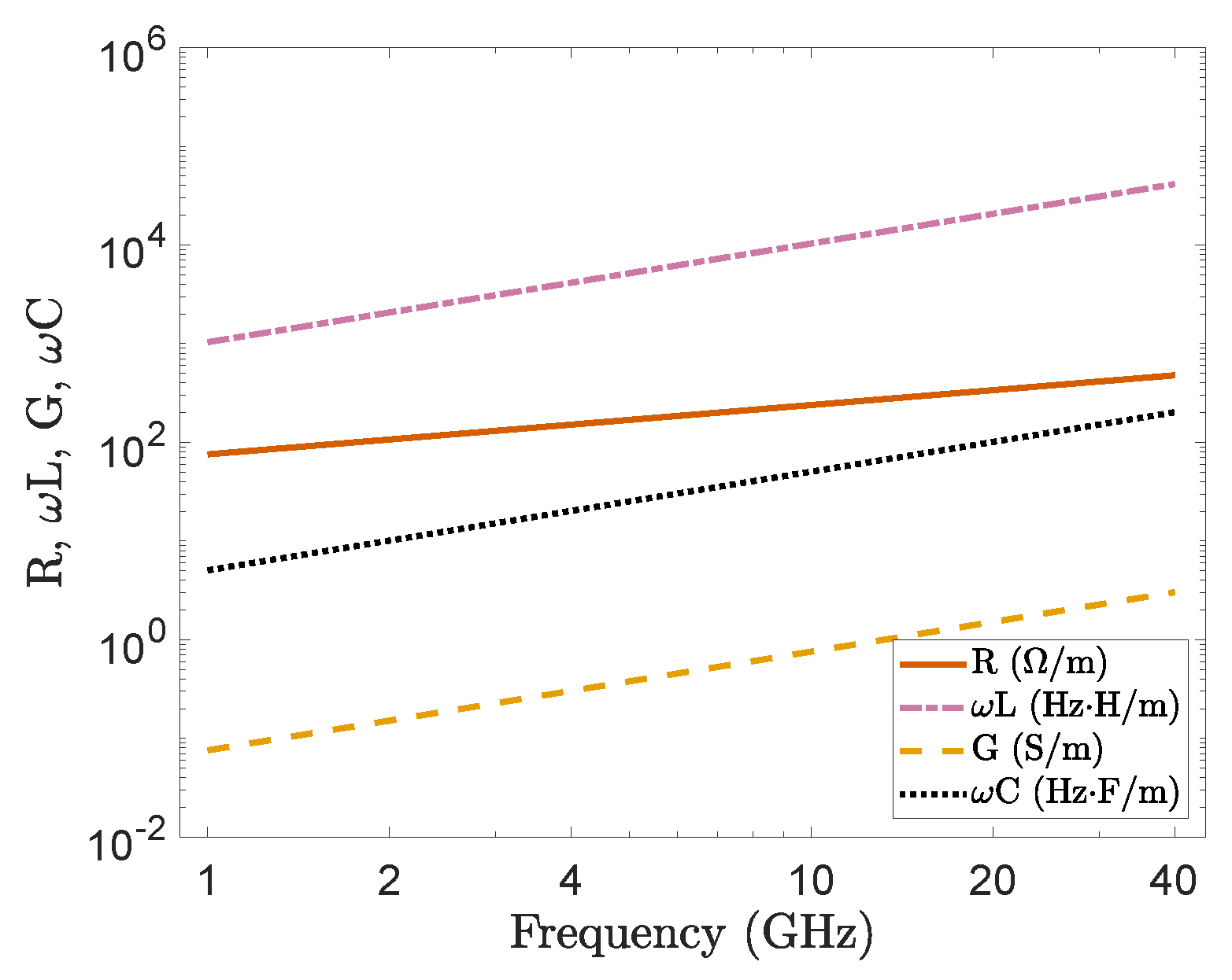
2. Theories of Coaxial TSVs

Considering the existing fabrication technologies, a coaxial-TSV prototype, as shown in the z plane in Figure 1a, is used as the baseline structure. The outside ground Cu shell has a radius of R D and a thickness of c = 10 μ m, and the central conductor has a cylinder radius of R d . A t-thick dielectric layer between the signal and ground conductors is required to provide both electrical isolation and mechanical support. Various materials including SiO 2 ( ε r = 3.9, tan δ = 0.003), Si 3 N 4 ( ε r = 7.5, tan δ = 0.003), benzocyclobutene (BCB, ε r = 2.7, tan δ = 0.001) [9], SU-8 ( ε r = 3.1, tan δ = 0.04) [32], Ajinomoto Build-up Film (ABF, ε r = 3.7, tan δ = 0.001), can be filled as the dielectric layer by using spin-coating or vapor deposition techniques. There is usually a shell of 0.1   μ m-thick SiO 2 as isolation layer between the dielectric layer and each conductor, which is ignored for simplicity of the modeling process. Similarly, the effect of the adhesion layer of Ti is also ignored in the following modeling and analysis.
Being a typical transmission line, the coaxial TSV can be described using the propagation constant γ and the characteristic impedance z C , or modeled with the per-unit-length (p.u.l) series resistance R, series inductance L, parallel capacitance C, and parallel conductance G [33]. In either approach, the corresponding parameters can be readily extracted from the scattering parameters of the coaxial TSV. Considering the small dimension and the low-frequency range, there is only TEM propagation mode in the coaxial TSV. In the microwave band, there is a skin depth δ s , which is frequency-dependent and is given as [34]
δ s = 2 ρ ω μ 0 μ r
where μ 0 is the permeability constant 4 π × 10 7 , μ r is the relative permeability (hereby assumed to be 1), and ρ is the bulk resistivity of the conductor. The resistivity of the most used copper metal is 1.673 × 10 8 Ω -m at 25 C , and thus, the skin depth of copper within the frequency range from 1 GHz to 40 GHz is 0.326   μ m to 2.059   μ m. When δ s is much smaller than the conductor thickness (usually at least 5 times the skin depth), the p.u.l series resistance R is calculated with
R = ρ / ( 2 π δ s ) R d + ρ / ( 2 π δ s ) R D
Whereas, when δ s is comparable to the conductor thickness, R is calculated with
R = ρ / ( 2 π δ s ) R d + δ s ( e R d δ s 1 ) + ρ / ( 2 π δ s ) c + δ s ( e c δ s 1 )
In order to calculate C, the cross-section of a coaxial-TSV structure can be located in the z plane in the way shown in Figure 1a. The circular structure in the z plane can be transformed to a rectangular structure in the t plane by using t = l n ( z ) . According to the theories of a parallel plate, the p.u.l capacitance C, together with the inductance L and conductance G, can be calculated by [35]
C = 2 π ε 0 ε r ln R D / R d
L = μ 0 μ r ln R D / R d 2 π
G = 2 π ε 0 ε r ω tan δ r ln R D / R d
where ε 0 and μ 0 are the vacuum permittivity and permeability, having the values of 8.854 × 10 12 and 4 π × 10 7 , respectively. As can be seen in Figure 2, within the frequency range from 1 GHz to 40 GHz, it always satisfies ω L R and ω C G ; hence, the characteristic impedance of a typical lossless coaxial line with a low-loss dielectric can be calculated with [35]
Z c = R + j ω L G + j ω C L C = μ 0 μ r ε 0 ε r ln ( R D / R d ) 2 π
According to Equation (7), adjusting the effective dielectric constant of the substrate is an important approach to reduce the outside conductor’s dimension of a 50 Ω coaxial TSV. As illustrated in the z plane of Figure 1b,c, the substrate materials with different dielectric constants can be inserted into the space between the inside and outside conductors in a ring-shape (forming a multi-layer coaxial structure) and a fan-shape. For the coaxial line with multi-layer or fan-shaped dielectrics as presented in Figure 1b,c, its p.u.l C can be respectively expressed as
C m u l = 2 π ε 0 ε 1 ε 2 ε 3 ε 2 ε 3 ln R 1 / R d + ε 1 ε 3 ln R 2 / R 1 + ε 1 ε 2 ln R D / R 2
C f a n = 2 π ε 0 ε 1 + π θ ε 0 ( ε 2 ε 1 ) / 90 ln R D / R d
where R 1 , R 2 , and R D are the outer radius of the dielectrics from inside to outside and the corresponding dielectric constants are ε 1 , ε 2 , and ε 3 , respectively. 2 θ is the angle of the fan-shaped area, where a substrate with a dielectric constant of ε 2 is used, while the dielectric constant of the left part is ε 1 . Since the permeability of all dielectrics hereby used is 1, the corresponding p.u.l L and R are the same as the typical coaxial TSV. Hence, the impedance calculation formulas of the multi-layer and fan-shaped coaxial TSVs are readily deduced. Furthermore, by combining with Equation (7), the effective dielectric constant of the substrate materials can also be easily obtained.
Validation analyses are performed using the FEM simulation, which is realized using the Ansys 3D High-Frequency Electromagnetic Simulation Software (HFSS). First, the impacts of dielectric material’s property on the values of characteristic impedance are analyzed. Simulations are performed on a typical coaxial TSV, whose R D is 57 μ m and R d is 25 μ m, while ε r and tan δ change from 1 to 12 and from 0 to 0.1, respectively. For simplicity, two wave ports are directly set at the two sides of the coaxial TSV. In the inset of Figure 3a, the simulated impedance is almost frequency-independent, and thus, an arbitrary frequency point at 39 GHz is used for comparison. The corresponding complex characteristic impedance of each simulated coaxial TSV is also calculated, by using the equations from (2) to (7), where R and G are considered.
As shown in Figure 3a,b, the magnitude of the calculated impedance is in very good agreement with the magnitude of the simulated characteristic impedance at 39 GHz. The difference for the dielectric constant and dielectric loss tangent between simulation and calculation are less than 0.26% and 0.16%, respectively. By comparing the magnitude and the real part of the characteristic impedance for both the calculated and the simulated results, it is noticed that the magnitude is almost the same as the real part of the simulated characteristic impedance, which validates that R and G in (7) are small enough to be ignored.
In order to validate the impedance calculation formulas of the coaxial TSVs with multi-layer dielectric materials, further simulations are performed on the above structure by using Si ( ε 1 and ε 3 ) and BCB ( ε 2 ). The TSV radius of the signal conductor is set at 25 μ m; the radius of the inner surface of the outside ground conductor is set at 53.4   μ m; the thickness of the outside ground conductor is 10 μ m; and the total height of the TSV structure is 200 μ m. First, the thickness of the sandwiched BCB ring is changed from 50 μ m to 90 μ m by adjusting R 2 and R D simultaneously, while the thicknesses of the two Si layers remain unchanged. Next, the BCB ring’s thickness is kept at 70 μ m, while its position is adjusted by changing R 1 (from 5 μ m to 35 μ m) and R 2 simultaneously [36]. As presented in Figure 3c,d, good agreements between simulation results and calculated values are achieved. Theory validation processes on the fan-shaped dielectric material-based coaxial TSVs are also carried out by using the simulation methods. Dimensions and parameters of the signal and ground conductors are set the same as the simulations for the multi-layer dielectric material-based structures. Parts of the silicon substrate between the signal and ground conductors are replaced with air, which form two fan-shaped areas. The characteristic impedance of a coaxial TSV with the two fan-shaped air areas are analyzed, whose angle θ is adjusted from 15 to 165 . As shown in Figure 3e, good agreement between the simulation and the calculation results are achieved. Generally, when the obtained characteristic impedance is too large, etching and removing a small part of the dielectric material can effectively reduce the desired impedance.

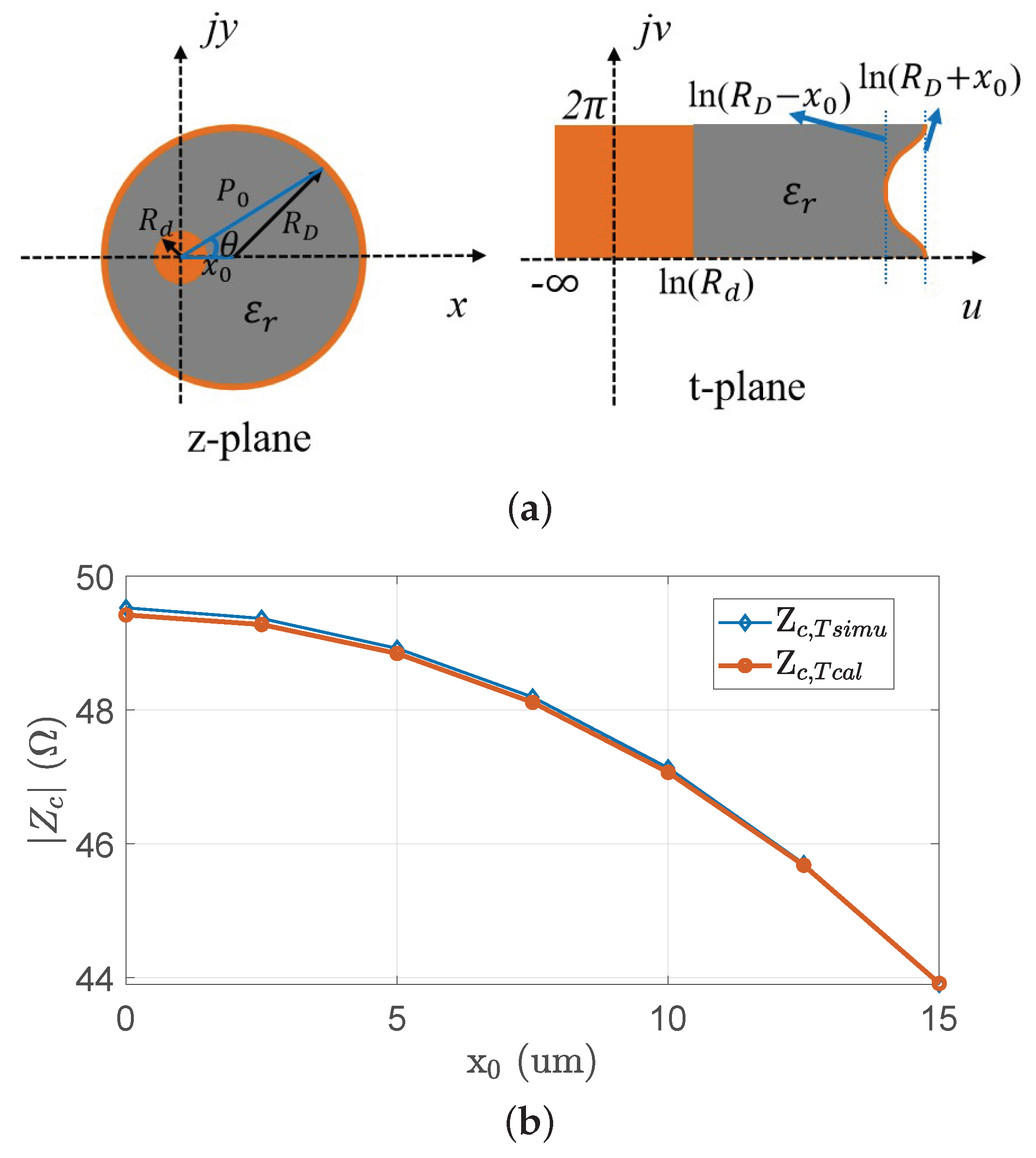
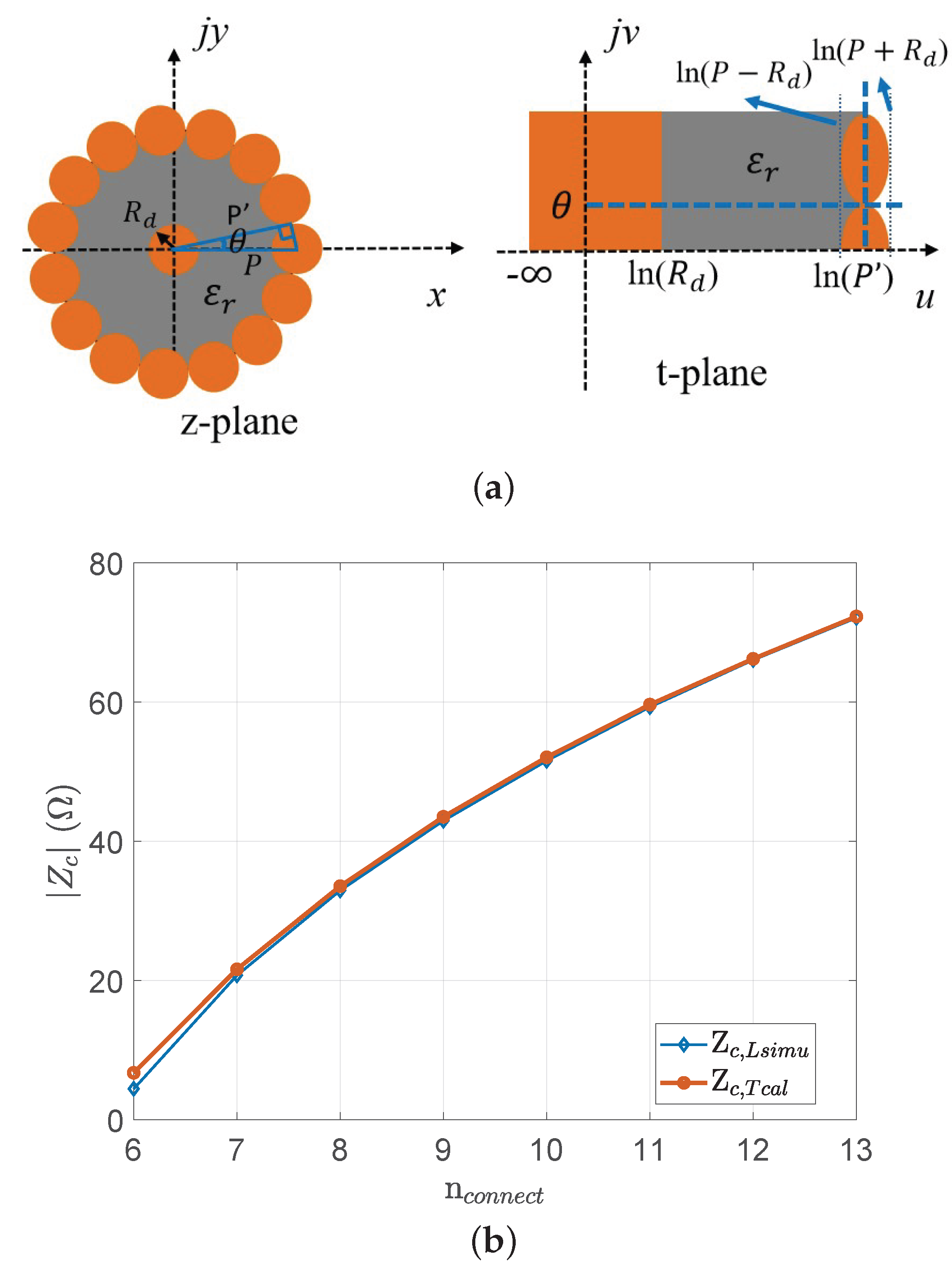
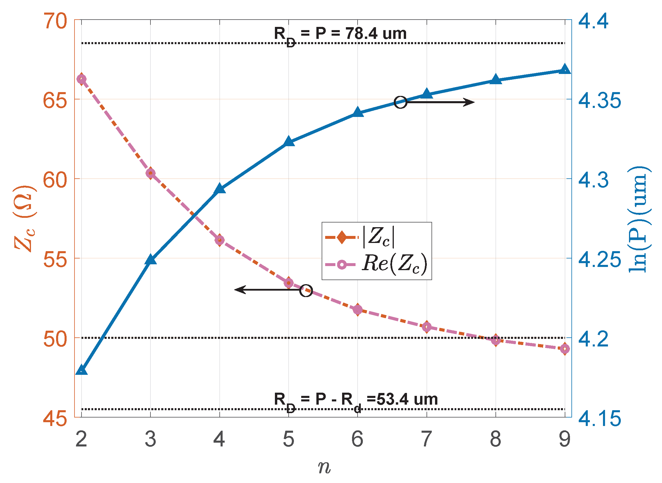
3. Coaxial-like TSVs

In a practical fabrication process, there is micromachining tolerance, which might result in a central deviation of the central signal conductor. As presented in the z plane in Figure 4a, the center of the signal conductor has been offset by x 0 along the X axis. θ is the angle between P 0 and the X axis, and P 0 is the actual distance between the center of the signal conductor and the inner surface of the outside conductor. Based on the transformation equation t = ln z , the structure in the z plane is transformed to a new geometry in the t plane, as seen in Figure 4a. It is seen that the inside surface of the outer conductor is no longer a straight line that is in parallel with t = ln R d . In this case, an effective R D e f f is needed to replace the position of R D , so that the impedance can still be calculated with (7). By using the image method for the cross-section of the coaxial-like TSV in the z plane, the effective R D e f f is obtained as follows
R D e f f = R D 2 + R d 2 x 0 2 + ( R D 2 + R d 2 x 0 2 ) 2 4 R D 2 R d 2 2 R D
In order to validate the impedance calculation theory of the off-centered coaxial line, FEM simulations are carried out with the center of the inner conductor being offset by x 0 = 0, 2.5, …, 15 μ m. The magnitudes of the simulated and calculated impedances are presented in Figure 4b. It is clear that the calculation results have shown very good agreement with the simulated values, which validates the reliability of the above theory. Generally, a nonlinear relationship is observed in Figure 4b, i.e., with larger offset values, a much more smaller characteristic impedance is obtained. This means that when off-centered coaxial TSV is often achieved in the manufacturing process, a larger R D might be considered to compensate the off-center effect of the inner-conducting TSV.
Sometimes, the ground of a TSV-structure-based coaxial line is fabricated by using a series of closely connected TSVs, as shown in Figure 5a. This can be used for the case when silicon substrate works as the dielectric material, and thus, the typical TSV manufacturing process can be used. For simplicity, the dielectric material is set as air in the following analytical process. Similar to the off-centered coaxial TSV, the transformed structure in the t plane in Figure 5a is complex, and thus, the effective inner radius R D e f f is also needed for calculating the characteristic impedance Z c of the connecting TSV-based structures. For this case, the effective inner radius R D e f f of the outside ground Cu shell can be calculated with
R D e f f = exp 1 arcsin ( R d P ) 0 arcsin ( R d P ) ln ( P 0 ) d θ
where P is the center distance between the central TSV and each outside TSV; P 0 is the actual distance between the center of the signal conductor and the inner surface of the outside conductor; θ is the angle between P 0 and the X axis, ranging from 0 to arcsin ( R d / P ) . P 0 in (11) can be calculated with
P 0 = P cos θ ( P cos θ ) 2 P 2 + R d 2
Next, the corresponding characteristic impedance of the special coaxial structures in the z plane of Figure 5a can be readily calculated with (7), by replacing R D with the corresponding R D e f f .
In order to validate the impedance calculation theory, FEM simulations are performed on a series of coaxial-like TSVs, with the TSV ( R d = 25 μ m) number n and the center distance P being listed in Table 1. Also given in Table 1 are the inner effective radius R D e f f of the connected-n-TSV-based ground conductor and the corresponding characteristic impedance, which are obtained using (7) and (11). The simulated and calculated impedance magnitudes are all shown in Figure 5b. Very good agreement between the calculation and simulation is observed, which validates the reliability of the above theories.
In a practical manufacturing procedure, ideally connecting TSVs might be difficult to realize, and thus, there might be a space between any two adjacent ground TSVs [21]. Therefore, two main groups of simulations are further performed on the coaxial-like TSVs, with the ground TSV number n increasing from 2 to 9. In both simulation groups, a cylinder Cu conductor with a radius of R d = 25 μ m is used as the TSV signal conductor and the TSV-based ground shell. In the first group of simulations, only n is adjusted while other parameters are maintained constant. The signal conductor and the ground shell are concentric, and the center distance P between the signal TSV and anyone of the ground TSV is set as 78.4   μ m. The simulated results are shown in Figure 6. Due to the low-loss property of the dielectric material, it is expected that the magnitude well overlaps the real part of the simulated impedance for the non-connecting ground TSV-based coaxial structure. Next, since the TSV center distance P and the TSV radius are kept at 78.4   μ m and 25 μ m, respectively, the impedance with the assumption of R D = P and R D = P R d can be calculated using (7). The impedance magnitudes are 68.53   Ω and 45.51   Ω , respectively, and are shown in Figure 6 as well. Clearly, it can be observed that the simulated impedance is always within the range from 45.51   Ω to 68.53   Ω , and, generally, larger Z c can be obtained with more ground TSVs when the TSV center distance is kept constant. Hence, an initial conclusion would be that the effective R D e f f seems to be within the range from P R d to P.
In the other simulation group, the cylindrical Cu TSVs still have a radius of R d = 25 μ m. While, aiming at maintaining Z c being always at 50 Ω , the TSV center distance P and the ground-TSV number n are adjusted simultaneously. When the number of ground TSVs increase from 2 to 9, the obtained TSV center distance P are 65.3   μ m, 70 μ m, 73.2   μ m, 75.4   μ m, 76.8   μ m, 77.7   μ m, 78.4   μ m, and 78.9   μ m, respectively. The TSV center distance in the natural logarithm form ln ( P ) at different ground-TSV numbers are presented in Figure 6. It can be noticed that there is a nonlinear relationship between ln ( P ) and n. Generally, for constant Z c , larger ln ( P ) is required when there are more ground TSVs. By comparing the results of the two analytical groups, it can be concluded that when the ground TSV number is determined, the larger TSV center distance P is related to a smaller characteristic impedance Z c , which is similar to the trend shown in (7).

4. Conclusions

In this paper, coaxial TSVs and coaxial-like TSVs are modeled and analyzed using the conformal mapping techniques and the FEM simulation. Due to the obvious importance in the impedance matching network for an efficient signal transition, the characteristic impedance of a TSV-based coaxial line is mainly focused. Apart from the typical coaxial-TSV structure, multi-layer dielectric-based and fan-shape dielectric-based coaxial TSVs are considered, and especially, the corresponding impedance calculation theories are provided. Generally, when the dimensions of the signal and ground conductors are fixed, replacing part of the silicon substrate using a low-loss dielectric material with a small dielectric constant can help decreasing the obtained characteristic impedance. Furthermore, considering the manufacturing procedure, coaxial-like TSVs can be analyzed. It can be noted that when the signal conductor is off-centered, a smaller characteristic impedance can be expected. Hence, the dimensions or the dielectric materials of the coaxial-like TSV should be accordingly adjusted, to realize an optimal high-frequency electrical performance. When using a series of connecting TSVs to work as the ground shell of the coaxial structure, a good impedance calculation formula is proposed by introducing an equivalent radius R D e f f . Though it is difficult to obtain the exact equations for analyzing the non-connection ground TSV-based coaxial-like structures, a primary conclusion can be drawn that a smaller TSV center distance P and fewer ground TSVs tend to provide a larger characteristic impedance Z c .

Author Contributions

Conceptualization, X.B. and Z.Z.; methodology, X.B., Z.Z. and J.L.; theories, H.Y., Z.W. and G.G.; simulation analysis, Z.Z. and H.Y.; validation and data analysis, X.B. and L.S.; writing—original draft preparation, X.B., Z.Z. and G.C.; writing—review and editing, N.D. and G.C.; supervision, X.B. and G.C. All authors have read and agreed to the published version of the manuscript.

Funding

The work is supported by the BIT Youth Academic Start-up Funding XSQD-202206001, in part by the National Key R&D Program of China (Grant no. 2022YFF0604801), and in part by the National Natural Science Foundation of China under Grant 62201037 and Grant 62271056.

Data Availability Statement

Not applicable.

Acknowledgments

The authors would like to acknowledge Yingtao Ding for the support in discussing the fabrication process. He works as a professor in the School of Integrated Circuits and Electronics, Beijing Institute of Technology, China.

Conflicts of Interest

The authors declare no conflict of interest.

Abbreviations

The following abbreviations are used in this manuscript:
TSVThrough-silicon-via
3DThree dimensional
RFRadio frequency
MEMSMicroelectromechanical Systems
S-GSignal-ground
DRIEDeep reactive ion etching
ARAspect ratio
BCBBenzocyclobutene
ABFAjinomoto Build-up Film
p.u.lper-unit-length
TEMTransverse Electromagnetic
FEMFinite Element Method

References

  1. Liu, X.; Sun, Q.; Huang, Y.; Chen, Z.; Liu, G.; Zhang, D.W. Optimization of TSV leakage in via-middle tsv process for wafer-level packaging. Electronics 2021, 10, 2370. [Google Scholar] [CrossRef]
  2. Ait Belaid, K.; Belahrach, H.; Ayad, H. Numerical laplace inversion method for through-silicon via (TSV) noise coupling in 3D-IC design. Electronics 2019, 8, 1010. [Google Scholar] [CrossRef] [Green Version]
  3. Tian, W.; Ma, T.; Liu, X. TSV technology and high-energy heavy ions radiation impact review. Electronics 2018, 7, 112. [Google Scholar] [CrossRef] [Green Version]
  4. Kim, J.; Pak, J.S.; Cho, J.; Song, E.; Cho, J.; Kim, H.; Song, T.; Lee, J.; Lee, H.; Park, K.; et al. High-frequency scalable electrical model and analysis of a through silicon via (TSV). IEEE Trans. Compon. Packag. Manuf. Technol. 2011, 1, 181–195. [Google Scholar]
  5. Xiong, W.; Dong, G.; Wang, Y.; Zhu, Z.; Yang, Y. 3-D Compact marchand balun design based on through-silicon via technology for monolithic and 3-D integration. IEEE Trans. Very Large Scale Integr. (VLSI) Syst. 2022, 30, 1107–1118. [Google Scholar] [CrossRef]
  6. Wang, Z. 3-D integration and through-silicon vias in MEMS and microsensors. J. Microelectromech. Syst. 2015, 24, 1211–1244. [Google Scholar] [CrossRef]
  7. Xu, Z.; Lu, J.Q. Three-dimensional coaxial through-silicon-via (TSV) design. IEEE Electron Device Lett. 2012, 33, 1441–1443. [Google Scholar] [CrossRef]
  8. Adamshick, S.; Coolbaugh, D.; Liehr, M. Feasibility of coaxial through silicon via 3D integration. Electron. Lett. 2013, 49, 1028–1030. [Google Scholar] [CrossRef]
  9. Jung, D.H.; Kim, H.; Kim, S.; Kim, J.J.; Bae, B.; Kim, J.; Yook, J.M.; Kim, J.C.; Kim, J. 30 Gbps high-speed characterization and channel performance of coaxial through silicon via. IEEE Microw. Wirel. Compon. Lett. 2014, 24, 814–816. [Google Scholar] [CrossRef]
  10. Wu, W.C.; Chang, E.Y.; Hwang, R.B.; Hsu, L.H.; Huang, C.H.; Karnfelt, C.; Zirath, H. Design, fabrication, and characterization of novel vertical coaxial transitions for flip-chip interconnects. IEEE Trans. Adv. Packag. 2009, 32, 362–371. [Google Scholar]
  11. Ho, S.W.; Rao, V.S.; Khan, O.K.N.; Yoon, S.U.; Kripesh, V. Development of coaxial shield via in silicon carrier for high frequency application. In Proceedings of the 2006 8th Electronics Packaging Technology Conference, Singapore, 6–8 December 2006; pp. 825–830. [Google Scholar]
  12. Yook, J.M.; Kim, Y.G.; Kim, W.; Kim, S.; Kim, J.C. Ultrawideband signal transition using quasi-coaxial through-silicon-via (TSV) for mm-wave IC packaging. IEEE Microw. Wirel. Compon. Lett. 2020, 30, 167–169. [Google Scholar] [CrossRef]
  13. Qian, L.; Xia, Y.; He, X.; Qian, K.; Wang, J. Electrical modeling and characterization of silicon-core coaxial through-silicon vias in 3-D integration. IEEE Trans. Compon. Packag. Manuf. Technol. 2018, 8, 1336–1343. [Google Scholar] [CrossRef]
  14. Shen, W.W.; Chen, K.N. Three-dimensional integrated circuit (3D IC) key technology: Through-silicon via (TSV). Nanoscale Res. Lett. 2017, 12, 56. [Google Scholar] [CrossRef] [PubMed] [Green Version]
  15. Yu, L.; Yang, H.; Jing, T.T.; Xu, M.; Geer, R.; Wang, W. Electrical characterization of RF TSV for 3D multi-core and heterogeneous ICs. In Proceedings of the 2010 IEEE/ACM International Conference on Computer-Aided Design (ICCAD), San Jose, CA, USA, 7–11 November 2010; pp. 686–693. [Google Scholar]
  16. Yook, J.M.; Kim, J.C.; Park, S.H.; Ryu, J.I.; Park, J.C. High density and low-cost silicon interposer using thin-film and organic lamination processes. In Proceedings of the 2012 IEEE 62nd Electronic Components and Technology Conference, San Diego, CA, USA, 29 May–1 June 2012; pp. 274–278. [Google Scholar]
  17. Malta, D.; Vick, E.; Goodwin, S.; Gregory, C.; Lueck, M.; Huffman, A.; Temple, D. Fabrication of TSV-based silicon interposers. In Proceedings of the 2010 IEEE International 3D Systems Integration Conference (3DIC), Munich, Germany, 16–18 November 2010; pp. 1–6. [Google Scholar]
  18. Bao, X.; Ocket, I.; Bao, J.; Doijen, J.; Zheng, J.; Kil, D.; Liu, Z.; Puers, B.; Schreurs, D.; Nauwelaers, B. Broadband dielectric spectroscopy of cell cultures. IEEE Trans. Microw. Theory Tech. 2018, 66, 5750–5759. [Google Scholar] [CrossRef]
  19. Bao, X.; Wang, L.; Wang, Z.; Zhang, J.; Zhang, M.; Crupi, G.; Zhang, A. Simple, fast, and accurate broadband complex permittivity characterization algorithm: Methodology and experimental validation from 140 GHz up to 220 GHz. Electronics 2022, 11, 366. [Google Scholar] [CrossRef]
  20. Ho, S.W.; Yoon, S.W.; Zhou, Q.; Pasad, K.; Kripesh, V.; Lau, J.H. High RF performance TSV silicon carrier for high frequency application. In Proceedings of the 2008 58th Electronic Components and Technology Conference, Lake Buena Vista, FL, USA, 27–30 May 2008; pp. 1946–1952. [Google Scholar]
  21. Chen, X.; Tang, J.; Xu, G.; Luo, L. Process development of a novel wafer level packaging with TSV applied in high-frequency range transmission. Microsyst. Technol. 2013, 19, 483–491. [Google Scholar] [CrossRef]
  22. Lee, W.C.; Min, B.W.; Kim, J.C.; Yook, J.M. Silicon-core coaxial through silicon via for low-loss RF Si-interposer. IEEE Microw. Wirel. Compon. Lett. 2017, 27, 428–430. [Google Scholar] [CrossRef]
  23. Farooq, M.; Graves-Abe, T.; Landers, W.; Kothandaraman, C.; Himmel, B.; Andry, P.; Tsang, C.; Sprogis, E.; Volant, R.; Petrarca, K.; et al. 3D copper TSV integration, testing and reliability. In Proceedings of the 2011 International Electron Devices Meeting, Washington, DC, USA, 5–7 December 2011; pp. 1–7. [Google Scholar]
  24. Hummler, K.; Smith, L.; Caramto, R.; Edgeworth, R.; Olson, S.; Pascual, D.; Qureshi, J.; Rudack, A.; Quon, R.; Arkalgud, S. On the technology and ecosystem of 3D/TSV manufacturing. In Proceedings of the 2011 IEEE/SEMI Advanced Semiconductor Manufacturing Conference, Saratoga Springs, NY, USA, 16–18 May 2011; pp. 1–6. [Google Scholar]
  25. Tippet, J.C.; Chang, D.C. Characteristic impedance of a rectangular coaxial line with offset inner conductor. IEEE Trans. Microw. Theory Tech. 1978, 26, 876–883. [Google Scholar] [CrossRef]
  26. Bao, X.; Crupi, G.; Ocket, I.; Bao, J.; Ceyssens, F.; Kraft, M.; Nauwelaers, B.; Schreurs, D. Numerical modeling of two microwave sensors for biomedical applications. Int. J. Numer. Model. Electron. Netw. Devices Fields 2021, 34, e2810. [Google Scholar] [CrossRef]
  27. Lukic, M.; Rondineau, S.; Popovic, Z.; Filipovic, S. Modeling of realistic rectangular/spl mu/-coaxial lines. IEEE Trans. Microw. Theory Tech. 2006, 54, 2068–2076. [Google Scholar] [CrossRef]
  28. Bao, X.; Ocket, I.; Bao, J.; Liu, Z.; Puers, B.; Schreurs, D.M.P.; Nauwelaers, B. Modeling of coplanar interdigital capacitor for microwave microfluidic application. IEEE Trans. Microw. Theory Tech. 2019, 67, 2674–2683. [Google Scholar] [CrossRef]
  29. Gugliandolo, G.; Tabandeh, S.; Rosso, L.; Smorgon, D.; Fernicola, V. Whispering gallery mode resonators for precision temperature metrology applications. Sensors 2021, 21, 2844. [Google Scholar] [CrossRef] [PubMed]
  30. Gugliandolo, G.; Naishadham, K.; Donato, N.; Neri, G.; Fernicola, V. Sensor-integrated aperture coupled patch antenna. In Proceedings of the 2019 IEEE International Symposium on Measurements & Networking (M&N), Catania, Italy, 8–10 July 2019; pp. 1–5. [Google Scholar]
  31. Gugliandolo, G.; Aloisio, D.; Campobello, G.; Crupi, G.; Donato, N. Development and metrological evaluation of a microstrip resonator for gas sensing applications. In Proceedings of the 24th IMEKO TC-4 International Symposium, Palermo, Italy, 14–16 September 2020; pp. 14–16. [Google Scholar]
  32. Bao, X.; Liu, S.; Ocket, I.; Bao, J.; Kil, D.; Zhang, S.; Cheng, C.; Feng, K.; Avolio, G.; Puers, B.; et al. Coplanar waveguide for dielectric material measurements at frequencies from 140 GHz to 220 GHz. In Proceedings of the 90th ARFTG Conference Digest, Boulder, CO, USA, 28 November–1 December 2017; pp. 1–4. [Google Scholar]
  33. Bao, X.; Liu, S.; Ocket, I.; Liu, Z.; Schreurs, D.M.; Nauwelaers, B.K. A modeling procedure of the broadband dielectric spectroscopy for ionic liquids. IEEE Trans. NanoBiosci. 2018, 17, 387–393. [Google Scholar] [CrossRef] [PubMed]
  34. Ong, N. Microwave cavity-perturbation equations in the skin-depth regime. J. Appl. Phys. 1977, 48, 2935–2940. [Google Scholar] [CrossRef]
  35. Costamagna, E.; Fanni, A. Characteristic impedances of coaxial structures of various cross section by conformal mapping. IEEE Trans. Microw. Theory Tech. 1991, 39, 1040–1043. [Google Scholar] [CrossRef]
  36. Li, Q.; Zhang, Y.; Qu, L.; Fan, Y. Quasi-static analysis of multilayer dielectrics filled coaxial line using conformal mapping method. In Proceedings of the 2018 IEEE International Conference on Computational Electromagnetics (ICCEM), Chengdu, China, 26–28 March 2018; pp. 1–3. [Google Scholar]
Figure 1. Schematics of the coaxial TSV in the z plane and the transformed t plane with (a) standard, (b) multi-layer, and (c) fan-shaped dielectric.
Electronics 11 03417 g001
Figure 2. The comparison of R and ω L and the comparison of G and ω C at frequencies from 1 GHz to 40 GHz, when R D , R D , and c are 57 μ m, 25 μ m, and 10 μ m, respectively, and the dielectric is silicon ( ε r = 11.9, tan δ = 0.015, and ρ 100 Ω -cm).
Electronics 11 03417 g002
Figure 3. Impacts on the characteristic impedance of the (a) dielectric constant and (b) dielectric loss tangent values of the single substrate, (c) thickness of a BCB ring inserted in a Si substrate, (d) position of a BCB ring in a Si substrate, and (e) angle of a fan-shaped air area in a Si substrate.
Electronics 11 03417 g003
Figure 4. (a) Schematics of the coaxial-like TSV in the z plane and the transformed t plane with off-centered inner conductor. (b) Comparison between simulated and calculated characteristic impedance of the off-centered coaxial-like TSV.
Electronics 11 03417 g004
Figure 5. (a) Schematics of the coaxial-like TSV in the z plane and the transformed t plane with TSV-based outside ground conductor. (b) Comparison between simulated and calculated characteristic impedance of connected-TSV-based coaxial-like TSVs, with the connected TSV number ranging from 6 to 13.
Electronics 11 03417 g005
Figure 6. Simulation results of coaxial-like TSVs with different ground-TSV number, where the left axis is the characteristic impedance (its magnitude is completely overlapped with its real part) and the right axis is the TSV center distance in the natural logarithmic form.
Electronics 11 03417 g006
Table 1. Calculated R D e f f and Z c C a l of the coaxial-like TSVs.
n678910111213
P ( μ m)50.0057.6265.3373.1080.9088.7496.59104.46
R D e f f ( μ m)28.1236.0243.7451.6459.5567.5775.3983.44
Z c C a l ( Ω )7.0521.8933.5443.5052.0559.6166.1872.26
Publisher’s Note: MDPI stays neutral with regard to jurisdictional claims in published maps and institutional affiliations.

