
On-Chip Bandstop to Bandpass Reconfigurable Filters Using Semiconductor Distributed Doped Areas (ScDDAs)
 , , ,
, , ,
Abstract
:1. Introduction
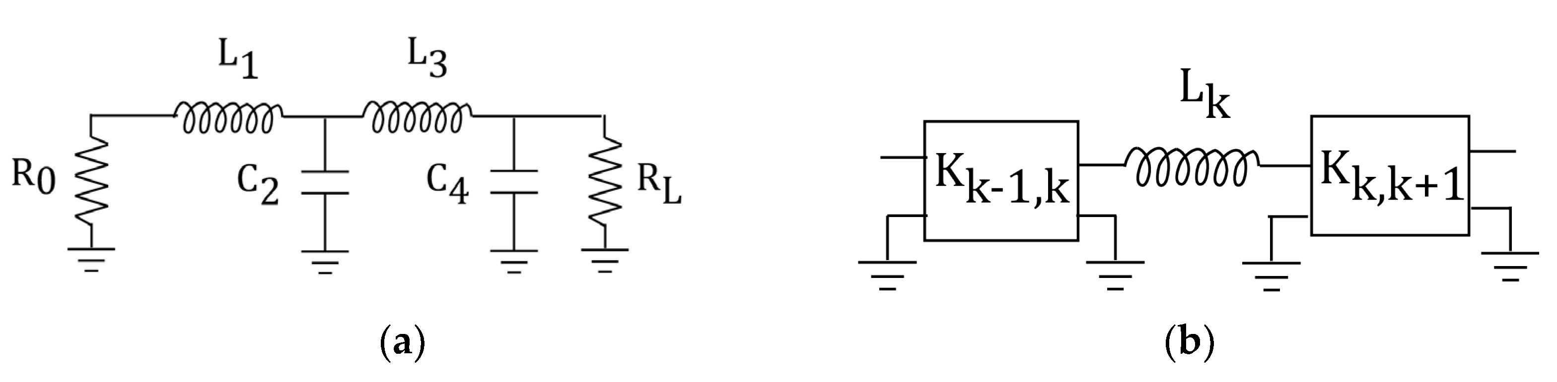
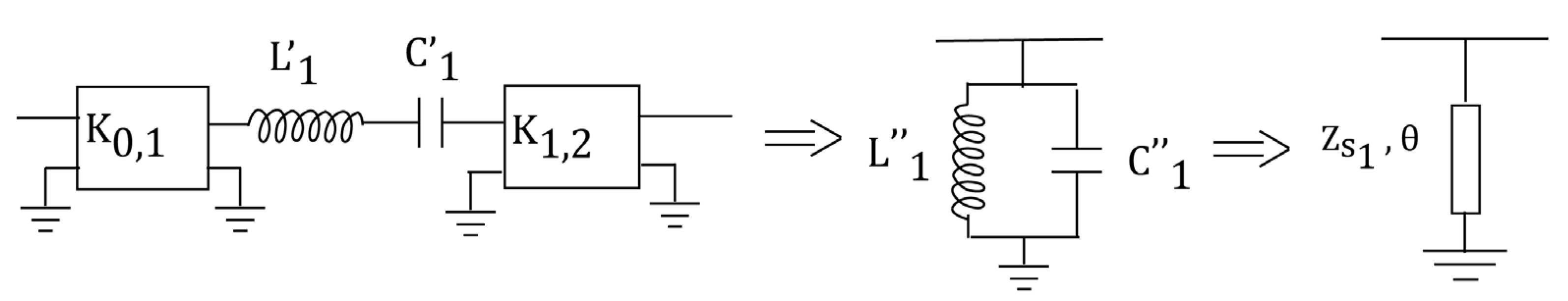
2. Synthesis
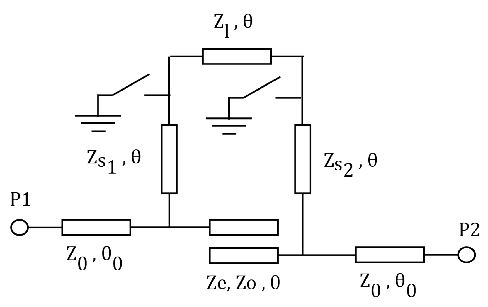
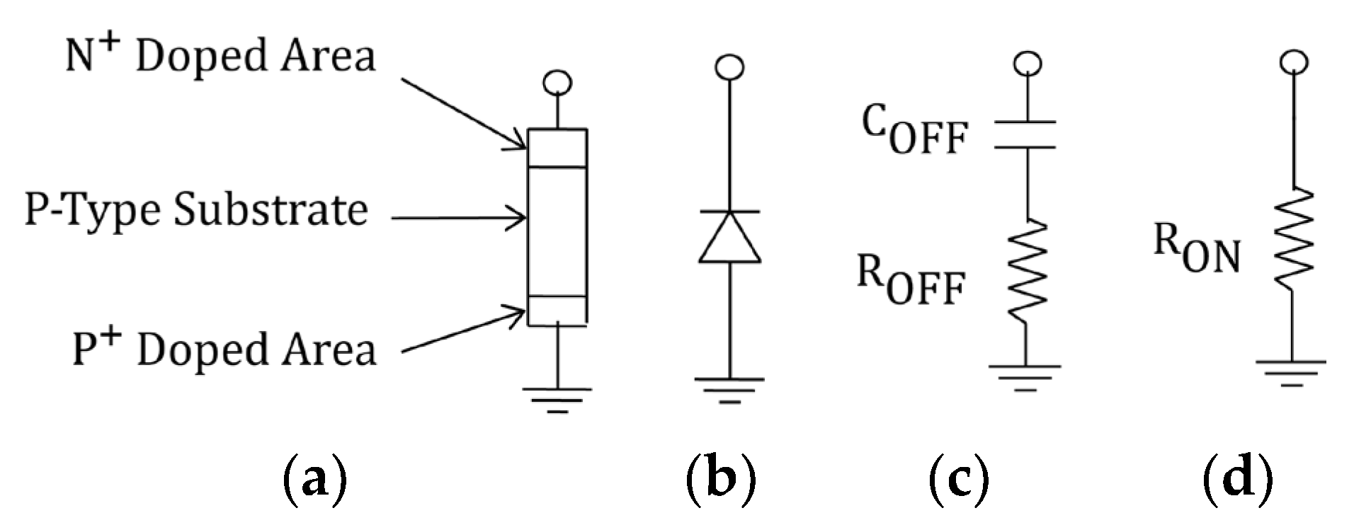
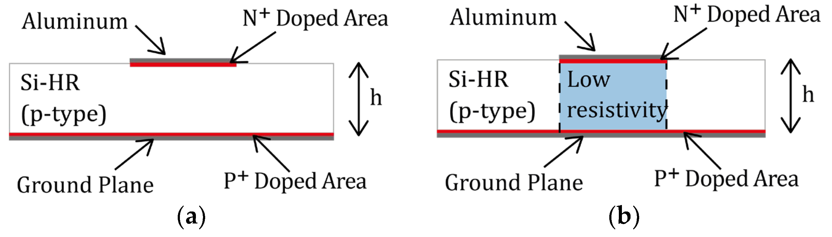
2.1. Reconfigurable Filter
2.2. Bandpass Filter
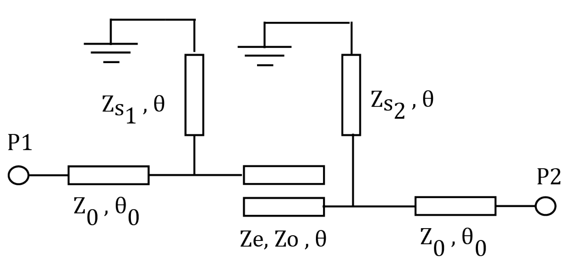
2.3. Bandstop Filter
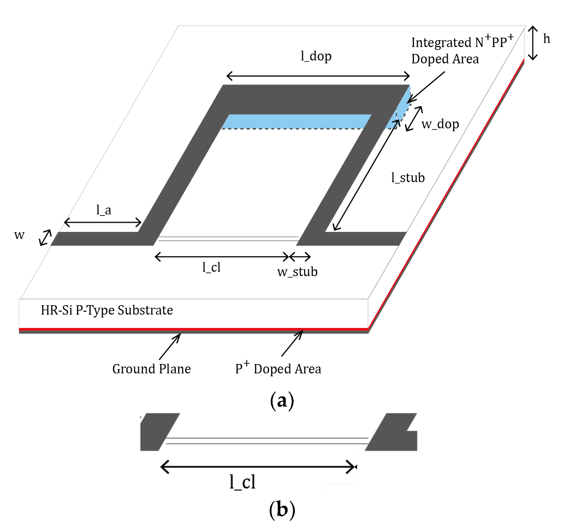
3. Reconfigurable Filter at 5 GHz
3.1. Concept and Simulations
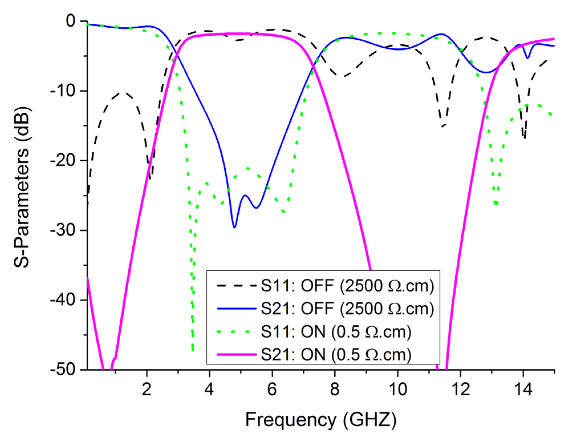
3.2. Measurement
4. The 10 GHz Reconfigurable Filter
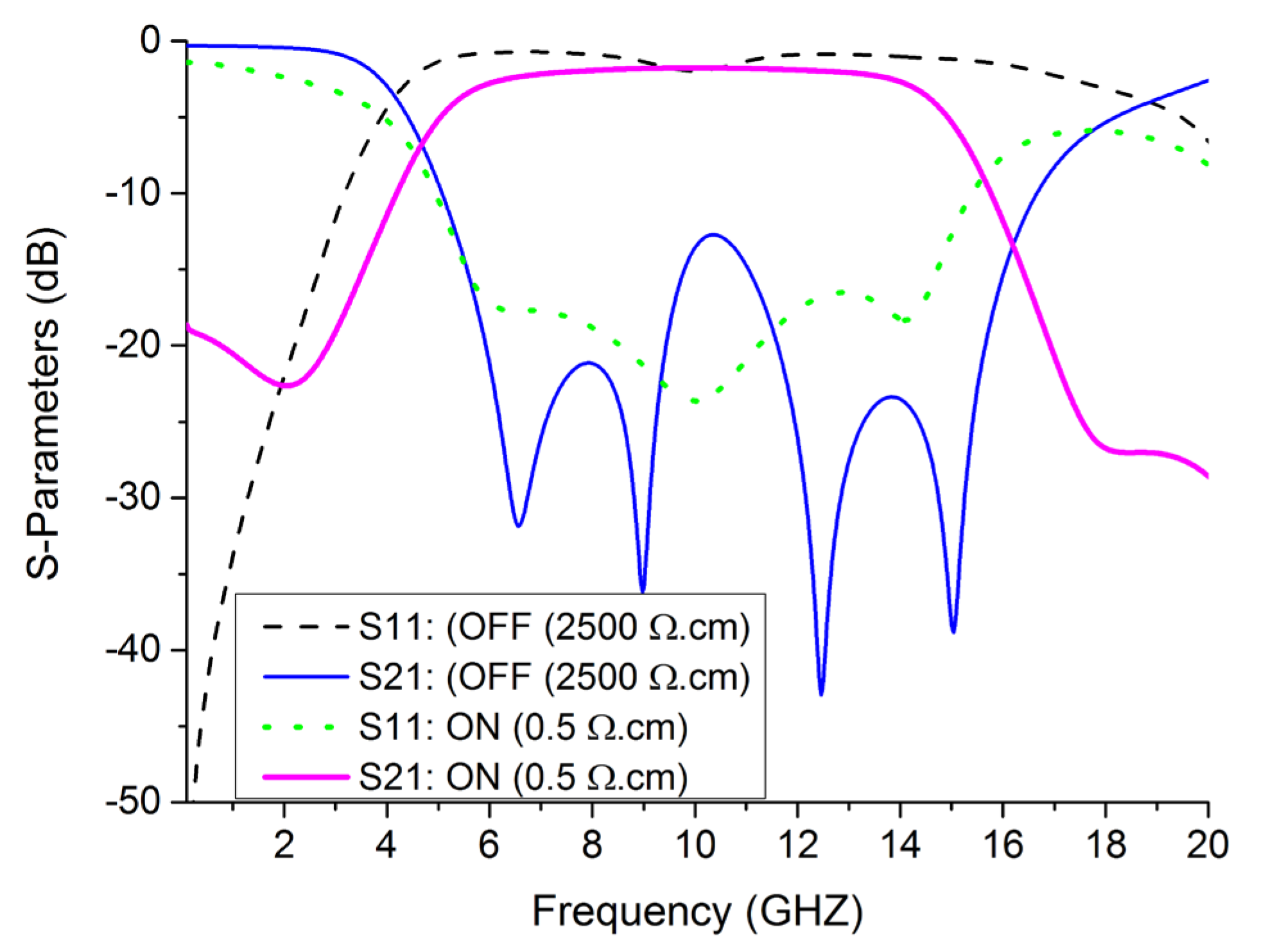
4.1. Design and Simulations
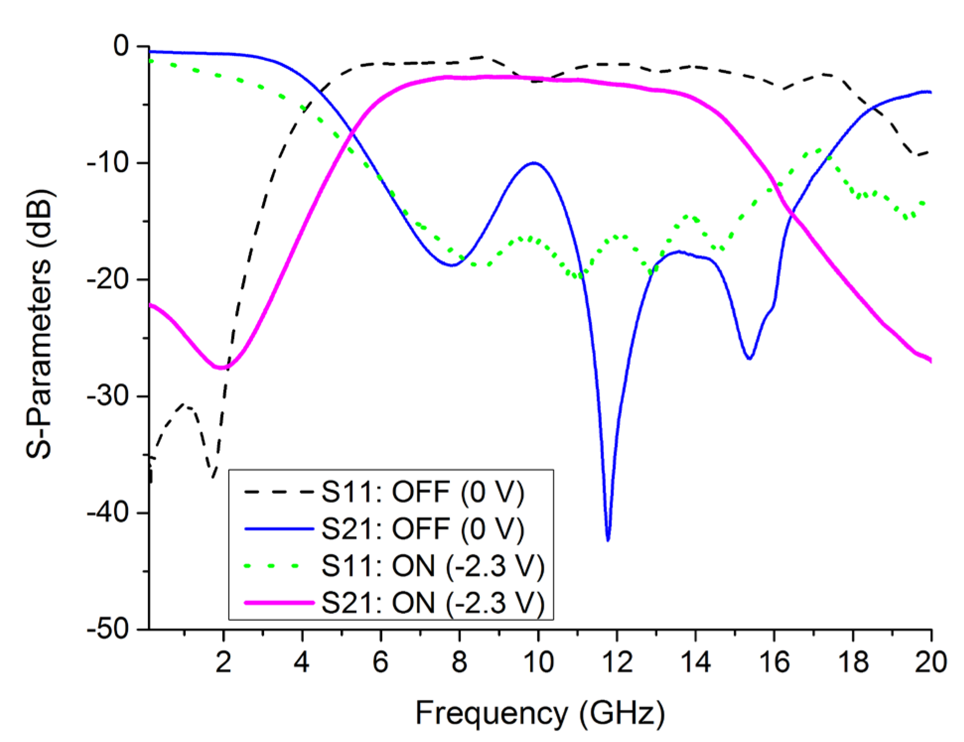
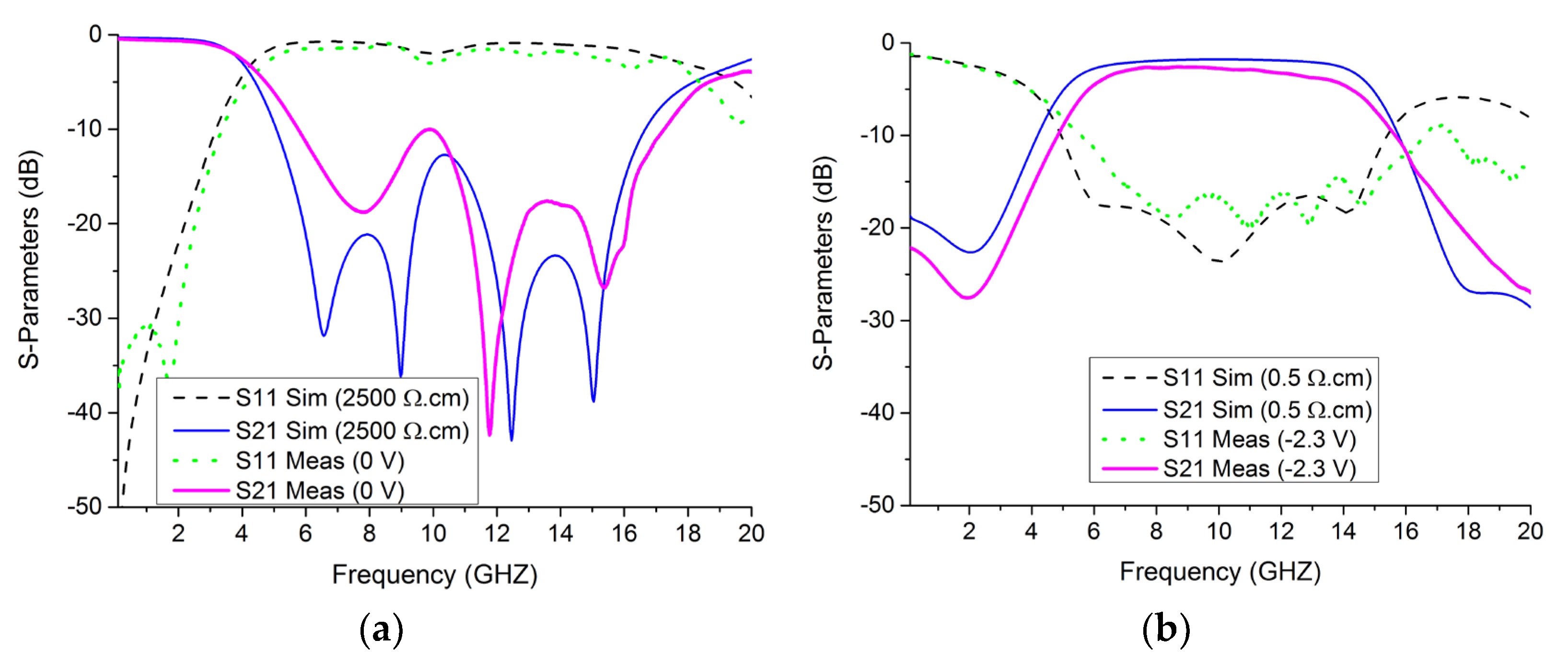
4.2. Measurement
5. Discussion
6. Conclusions
Author Contributions
Funding
Data Availability Statement
Conflicts of Interest
References
- Gentili, F.; Cacciamani, F.; Nocella, V.; Sorrentino, R.; Pelliccia, L. RF MEMS hairpin filter with three reconfigurable bandwidth states. In Proceedings of the 2013 European Microwave Conference, Nuremberg, Germany, 6–10 October 2013; pp. 802–805. [Google Scholar] [CrossRef]
- Bouyge, D.; Crunteanu, A.; Pothier, A.; Martin, P.O.; Blondy, P.; Velez, A.; Bonache, J.; Orlianges, J.C.; Martin, F. Reconfigurable 4 pole bandstop filter based on RF-MEMS-loaded split ring resonators. In Proceedings of the 2010 IEEE MTT-S International Microwave Symposium, Anaheim, CA, USA, 23–28 May 2010; pp. 588–591. [Google Scholar] [CrossRef]
- Blondy, P.; Palego, C.; Houssini, M.; Pothier, A.; Crunteanu, A. RF-MEMS Reconfigurable Filters on Low Loss Substrates for Flexible Front Ends. In Proceedings of the 2007 Asia-Pacific Microwave Conference, Bangkok, Thailand, 11–14 December 2007; pp. 1–3. [Google Scholar] [CrossRef]
- Araujo, L.d.; de Oliveira, A.J.B.; Llamas-Garro, I.; Mira, F.; Lancaster, M.J. Reconfigurable Microwave Coupled Resonator Band-pass Filter and Diplexer. In Proceedings of the 2019 SBMO/IEEE MTT-S International Microwave and Optoelectronics Conference (IMOC), Aveiro, Portugal, 10–14 November 2019; pp. 1–3. [Google Scholar] [CrossRef]
- Cheng, T.; Tam, K. A Wideband Bandpass Filter With Reconfigurable Bandwidth Based on Cross-Shaped Resonator. IEEE Microw. Wirel. Compon. Lett. 2017, 27, 909–911. [Google Scholar] [CrossRef]
- Simpson, D.J.; GÓmez-García, R.; Psychogiou, D. Tunable Multiband Bandpass-to-Bandstop RF Filters. In Proceedings of the 2018 IEEE/MTT-S International Microwave Symposium-IMS, Philadelphia, PA, USA, 10–15 June 2018; pp. 1363–1366. [Google Scholar] [CrossRef]
- Zahari, M.K.; Shairi, N.A.; Ahmad, B.H.; Zakaria, Z.; Wong, P.W. Miniaturized Switchable Bandpass to Matched Bandstop Filter Using Stepped-Impedance Resonator. In Proceedings of the 2018 IEEE International Workshop on Electromagnetics: Applications and Student Innovation Competition (iWEM), Nagoya, Japan, 29–31 August 2018; pp. 1–2. [Google Scholar] [CrossRef]
- Song, K.; Chen, W.; Patience, S.R.; Chen, Y.; Iman, A.M.; Fan, Y. Compact Wide-Frequency Tunable Filter With Switchable Bandpass and Bandstop Frequency Response. IEEE Access 2019, 7, 47503–47508. [Google Scholar] [CrossRef]
- Zahari, M.K.; Ahmad, B.H.; Wong, P.W.; Shairi, N.A. Switchable bandstop to bandpass filter using parallel-coupled resonator. In Proceedings of the 2017 IEEE Asia Pacific Microwave Conference (APMC), Kuala Lumpur, Malaysia, 13–16 November 2017; pp. 513–516. [Google Scholar] [CrossRef]
- Kumar, N.; Singh, Y.K. Switchable compact widestopband bandstop filter to wideband bandpass filter. In Proceedings of the 2015 Asia-Pacific Microwave Conference (APMC), Nanjing, China, 6–9 December 2015; pp. 1–3. [Google Scholar] [CrossRef]
- Zhu, H.-R.; Ning, X.-Y.; Huang, Z.-X.; Wu, X.-L. An Ultra-Compact On-Chip Reconfigurable Bandpass Filter With Semi-Lumped Topology by Using GaAs pHEMT Technology. IEEE Access 2020, 8, 31606–31613. [Google Scholar] [CrossRef]
- Bergeras, F.; Duême, P.; Plaze, J.; Darcel, L.; Jarry, B.; Campovecchio, M. Novel MMIC architectures for tunable microwave wideband active filters. In Proceedings of the 2010 IEEE MTT-S International Microwave Symposium, Anaheim, CA, USA, 23–28 May 2010; pp. 1356–1359. [Google Scholar] [CrossRef]
- Shahid, I.; Thalakotuna, D.N.; Karmokar, D.K.; Mahon, S.J.; Heimlich, M. A Compact Reconfigurable 1-D Periodic Structure in GaAs MMIC With Stopband Switching, Dual-Band Operation and Tuning Capabilities. IEEE Access 2021, 9, 142084–142094. [Google Scholar] [CrossRef]
- Allanic, R.; le Berre, D.; Quéré, Y.; Quendo, C.; Chouteau, D.; Grimal, V.; Valente, D.; Billoué, J. Three-State Microwave Tunable Resonator Integrating Several Active Elements on Silicon Technology in a Global Design. IEEE Microw. Wirel. Compon. Lett. 2018, 28, 141–143. [Google Scholar] [CrossRef]
- Allanic, R.; le Berre, D.; Quéré, Y.; Quendo, C.; Chouteau, D.; Grimal, V.; Valente, D.; Billoué, J. Continuously Tunable Resonator Using a Novel Triangular Doped Area on a Silicon Substrate. IEEE Microw. Wirel. Compon. Lett. 2018, 28, 1095–1097. [Google Scholar] [CrossRef]
- Allanic, R.; le Berre, D.; Quendo, C.; Chouteau, D.; Grimal, V.; Valente, D.; Billoué, J. A Novel Synthesis for Bandwidth Switchable Bandpass Filters Using Semi-Conductor Distributed Doped Areas. IEEE Access 2020, 8, 122599–122609. [Google Scholar] [CrossRef]
- Allanic, R.; le Berre, D.; Quendo, C.; Chouteau, D.; Grimal, V.; Valente, D.; Billoué, J. Switchable DBR Filters Using Semiconductor Distributed Doped Areas (ScDDAs). Electronics 2020, 9, 2021. [Google Scholar] [CrossRef]
- Allanic, R.; le Berre, D.; Quendo, C.; Chouteau, D.; Grimal, V.; Valente, D.; Billoué, J. Frequency Reconfigurable Interdigital Filter Using Semi-conductor Distributed Doped Areas. In Proceedings of the 2019 IEEE Asia-Pacific Microwave Conference (APMC), Singapore, 10–13 December 2019; pp. 974–976. [Google Scholar] [CrossRef]
- Sanchez-Soriano, M.Á.; Torregrosa-Penalva, G.; Bronchalo, E. Compact Wideband Bandstop Filter With Four Transmission Zeros. IEEE Microw. Wirel. Compon. Lett. 2010, 20, 313–315. [Google Scholar] [CrossRef]
- Feng, W.; Shang, Y.; Che, W.; Gómez-García, R.; Xue, Q. Multifunctional Reconfigurable Filter Using Transversal Signal-Interaction Concepts. IEEE Microw. Wirel. Compon. Lett. 2017, 27, 980–982. [Google Scholar] [CrossRef]
- Matthaei, G.L.; Young, L.; Jones, E.M.T. Microwave Filters, Impedance-Matching Networks, and Coupling Structures; McGraw-Hill Book Company, Inc.: Norwood, MA, USA, 1964; Volume 1, ISBN 9780890060995. [Google Scholar]
- Ponchak, G.E. RF Transmission Lines on Silicon Substrates. In Proceedings of the 1999 29th European Microwave Conference, Munich, Germany, 5–7 October 1999; pp. 158–161. [Google Scholar] [CrossRef] [Green Version]


| n | g0 | g1 | g2 | g3 | g4 | g5 | |
|---|---|---|---|---|---|---|---|
| 4 | 1 | 0.7128 | 1.2003 | 1.3212 | 0.6476 | 1.1007 | 1 |
| L1 | L2 | L3 | L4 | L′2 | L′3 | K0,1 | K2,3 | Z2 | Z3 |
|---|---|---|---|---|---|---|---|---|---|
| 35.6 | 60 | 66 | 40.5 | 2.73 × 10⁻⁹ | 3 × 10⁻⁹ | 50 | 50 | 67 | 74 |
| Za | Zo | Ze | Zs1 | Zs2 | Zl |
|---|---|---|---|---|---|
| 50 Ω | 74 Ω | 174 Ω | 39 Ω | 41 Ω | 31 Ω |
| Access | l_a = 3.18 mm | w = 0.54 mm |
| Coupled line | l_cl = 5.34 mm | w_cl = 0.02 mm s = 0.14 mm |
| Stub1 | l_stub1 = 4.57 mm | w_stub1 = 0.9 mm |
| Stub2 | l_stub2 = 4.57 mm | w_stub2 = 0.82 mm |
| Doped area | l_dop = 7.26 mm | w_dop = 1.15 mm |
| L1 | L2 | L3 | L4 | L′2 | L′3 | K0,1 | K2,3 | Z2 | Z3 |
|---|---|---|---|---|---|---|---|---|---|
| 35.6 | 60 | 66 | 33.7 | 9.6 × 10⁻¹⁰ | 1.05 × 10⁻⁹ | 50 | 50 | 47 | 52 |
| Za | Zo | Ze | Zs1 | Zs2 | Zl |
|---|---|---|---|---|---|
| 50 Ω | 52 Ω | 152 Ω | 55 Ω | 58 Ω | 64 Ω |
| Access | l_a = 3.61 mm | w = 0.55 mm |
| Coupled line | l_cl = 2.6 mm | w_cl = 0.05 mm s = 0.1 mm |
| Stub1 | l_stub1 = 2.4 mm | w_stub1 = 0.46 mm |
| Stub2 | l_stub2 = 2.4 mm | w_stub2 = 0.39 mm |
| Doped area | l_dop = 3.55 mm | w_dop = 0.3 mm |
| Ref. | Frequency | Reconfigurability Method | States-Number | IL in Bandpass Mode | In-Band Rejection in Bandstop Mode | Electrical Dimensions |
|---|---|---|---|---|---|---|
| [6] | 0.9–1.6 GHz | 4 trimmer caps and 4 pin diodes | 2 bands in the BPF 4 bands in the BSF | <0.92 dB | >26.5 dB | Not indicated |
| [7] | 2.4 GHz | 2 pin diodes | 2 | 4.3 dB | 38 dB | |
| [8] | 1 GHz | 2 pin diodes and 3 varactors | continuous | 4.7 dB < IL < 5.6 dB | >13 dB | |
| [9] | 2.4 GHz | 2 pin diodes | 2 | 10 dB | 30 dB | |
| [10] | 1 GHz | 2 pin diodes | 2 | * 1 dB | * 22 dB | |
| This study | 5 GHz | ScDDA | 2 | 2.7 dB | >16 dB | |
| This study | 10 GHz | ScDDA | 2 | 2.6 dB | >10 dB |
Publisher’s Note: MDPI stays neutral with regard to jurisdictional claims in published maps and institutional affiliations. |
© 2022 by the authors. Licensee MDPI, Basel, Switzerland. This article is an open access article distributed under the terms and conditions of the Creative Commons Attribution (CC BY) license (https://creativecommons.org/licenses/by/4.0/).
Share and Cite
Allanic, R.; Le Borgne, F.; Bouazzaoui, H.; Le Berre, D.; Quendo, C.; Silva De Vasconcellos, D.; Grimal, V.; Valente, D.; Billoué, J. On-Chip Bandstop to Bandpass Reconfigurable Filters Using Semiconductor Distributed Doped Areas (ScDDAs). Electronics 2022, 11, 3420. https://doi.org/10.3390/electronics11203420
Allanic R, Le Borgne F, Bouazzaoui H, Le Berre D, Quendo C, Silva De Vasconcellos D, Grimal V, Valente D, Billoué J. On-Chip Bandstop to Bandpass Reconfigurable Filters Using Semiconductor Distributed Doped Areas (ScDDAs). Electronics. 2022; 11(20):3420. https://doi.org/10.3390/electronics11203420
Chicago/Turabian StyleAllanic, Rozenn, Fabien Le Borgne, Hassan Bouazzaoui, Denis Le Berre, Cédric Quendo, Douglas Silva De Vasconcellos, Virginie Grimal, Damien Valente, and Jérôme Billoué. 2022. "On-Chip Bandstop to Bandpass Reconfigurable Filters Using Semiconductor Distributed Doped Areas (ScDDAs)" Electronics 11, no. 20: 3420. https://doi.org/10.3390/electronics11203420