
2-Mbps Power-Line Communication Transmitter Based on Switched Capacitors for Automotive Networks

1
Department of Physics “G. Occhialini”, University of Milano Bicocca, 20126 Milan, Italy
2
Melexis GmbH, 99099 Erfurt, Germany
*
Author to whom correspondence should be addressed.
Electronics 2022, 11(22), 3651; https://doi.org/10.3390/electronics11223651
Submission received: 19 October 2022
/
Revised: 3 November 2022
/
Accepted: 4 November 2022
/
Published: 8 November 2022
(This article belongs to the Special Issue Vehicular Communication Based on Networks)
Abstract
:Nowadays, automotive wire harnesses have become very complex systems as the number of electronic components and Electronic Control Units (ECUs) inside a vehicle have increased dramatically. To manage this complexity, and to support the automotive systems of tomorrow, new communication techniques need to be investigated. In this work, a direct modulated Power-Line Communication (PLC) method is proposed to drastically reduce the number of interconnections and give advantages in cost, complexity, and weight. Two transmitter topologies based on a Switching Capacitor approach are presented and implemented in a Test Chip fabricated in a 180 nm HV-CMOS SOI technology. The proposal is validated by communication tests connecting the designed chip and a discrete component-based demonstrator receiver through an unshielded twisted pair cable. Compared to commercially available solutions, the proposed approach can reach a data rate of 2 Mbps, making it able to implement high-speed event-driven networks, such as the Controller Area Network (CAN).
1. Introduction
The automotive industry is living a big transformation as even more tasks are entrusted to electric and electronic systems. This allows carmakers to improve safety, comfort, and entertainment and to introduce new functions such as Advanced Driver-Assistance Systems (ADAS). According to forecasts, electronics account for about 80% of automotive innovation, and vehicle electronic content growth will reach 50% by 2030 [1,2]. Electronic systems and subsystems are distributed over the entire vehicle and are controlled by dedicated modules named Electronic Control Units (ECUs). Besides the power supply, ECUs need one or more communication cables and usually an addressing line. The number of ECUs in a single vehicle is constantly increasing, and there can be up to 150 of them in a modern car. As a result, the number of interconnections is raised, and the wiring harness complexity, weight, and cost increase, making it one of the most critical blocks to design [3]. A physical merge of the supply and communication lines can drastically reduce the amount of needed cables and provide enormous benefits. The feasibility of Power-Line Communication (PLC) systems in an automotive environment has already been proven by commercially available proposals based on a carrier modulation [4,5,6]. However, the resulting data rate ≤500 kbps and latency would disable the use in high-speed event-driven applications (≥1 Mbps), such as the Controller Area Network (CAN) [7]. Therefore, a base-band PLC system is examined to realize a CAN protocol with a modified physical layer. In this work, two transmitter circuits are presented, and are validated by a prototype implemented in a 180 nm HV-CMOS SOI technology.
Concept and proposed transmitter topologies are described in Section 2. Detailed circuit implementation is presented in Section 3. In Section 4, the fabricated Test Chip is shown. Simulation setup and measurements results follow in Section 5, validating the proposals, and Section 6 concludes the paper.
2. Switched-Capacitor Transmitter Topologies
In the proposed PLC system, the power supply for the connected nodes is embedded in the data connection lines. Thus, a coupling feed from the power source is needed to separate it from the communication channel [8]. All devices connected to the bus are supplied via an inductive feed that reduces high current variations. The basic concept is to inject defined charges on the transmission line to obtain signal pulses for the communication [9]. Two different transmitter topologies based on switching capacitors are proposed in Section 2.1 and Section 2.2 to fulfill this task.
To understand the principle of the charge injection, and to evaluate some design specifications, the discharge phase of a functional Switching Capacitor is studied. In Figure 1, the equivalent s-domain model of a charge injection event is shown. is connected by a switch with finite on-resistance to the transmission line. The line has characteristic impedance , and it is terminated by resistor . The capacitance associated with the physical implementation aspects is also included. Finally, the coupling feed is composed of and . In the following analysis, the inductance is assumed to be sufficiently high so that at 10 MHz. Assuming that the capacitor is initially charged to the DC supply level , the pulse waveform of a discharge event can be evaluated by solving the inverse Laplace transform of the presented scheme [10]:
The peak voltage, the rising (), and falling () time constants are:
with
and . Simulation results with different sizes of are shown in Figure 2, where it has been assumed to design a switch with and, , pF, H, V.
It can be deduced that switching capacitor ≤2 nF is required to reach a data rate of 2 Mbps (falling time 100 ns). To ensure communication robustness, also needs to be at least one order higher than , i.e., ≥100 pF. Therefore, a trade-off between switching capacitor size and data rate is shown. This analysis leads to considering external capacitor in the developed proposal, both for the area occupation and for the higher flexibility.
2.1. H-Bridge Topology
The first transmitter topology is the H-Bridge implementation of Figure 3. The supply is applied on the transmission line through the coupling feed composed of and . Moreover, the line is terminated by an AC-coupling capacitor () and two series resistors.
The circuit consists of a switching capacitor (), which can be connected to the transmission line through two equal High-Side Switches (HSS), and , and two equal Low-Side Switches (LSS), and , which operate in an H-Bridge topology. The circuit commutes among three possible states, as described in Table 1, which are alternating at each received data edge. Assuming that is initially discharged, at the first Charge-State (e.g., Charge 1–4), it is charged to . As a guard against overlap and unwanted cross currents between the transmission rails, an Open-State is always placed after a charge event, during which the charge in is preserved. As the next step, the second Charge-State (e.g., Charge 2–3) is reconnecting the capacitor to the transmission line, and is charging it to . As illustrated in Figure 4, a drop in the differential transmission line occurs for each edge of received data as a result of the charge transferred from the line itself to .
The obtained timing constant (), and the average current consumption () can be evaluated as follows:
where DR is the data rate. The transmitted signal is unipolar and thus a pre-coding is needed since falling or rising edges of the data signal cannot be distinguished. Hence, for an uncoded data stream applied to the TX, the protocol frame structure needs to be taken into account so that a message header such as in [11] can be used to assign the correct data polarity. However, the simplest encoding to resolve the ambiguity is to encode the data as a unipolar Return-to-Zero (RZ) stream [12].
2.2. 3-Switches Topology
The second proposed transmitter topology is the 3-Switches SC scheme of Figure 5 where two capacitors (, ) are charged and discharged according to the three possible states described in Table 2. During the Charge-State, and are charged in parallel through (HSS) and (LSS) to , where . In the next step, the capacitors are discharged in series through (Floating Switch, FS) to . Similar to the H-Bridge, an Open-State is placed in between to avoid cross currents, during which the charges are preserved. As a result, as shown in Figure 6, positive and negative pulses appear on the differential transmission line, so the data polarity can be recovered directly. Unlike the H-Bridge, the states are not symmetrical, and the charging () and discharging () timing constants are not equal:
The average current consumption () can be evaluated as
and, assuming that the same data rate and capacitors size are used, is 8-times less than in the previous approach.
3. Switch Implementations
Transmitter operation requires proper switch functions. The proposed schemes of Figure 3 and Figure 5 require efficient low-side switch (LSS) (connected to ground), high-side switch (HSS) (connected to ), and floating switch (FS) (i.e., not connected to ground or ). According to Equations (5), (7) and (8), switches with on-resistance of ≤10 are required to reach a data rate of 2 Mbps if switching capacitors of 1 nF are used. The design is made in a technology which includes HV (High-Voltage) devices up to 40 V and LV (Low-Voltage) devices up to 5 V. Both the HV and the LV devices have a gate-source voltage range between −5.5 V and 5.5 V, which must be guaranteed for safe operations. The circuits share a common current master mirror fed by a 10 A current provided by the Supply System of the designed chip.
3.1. Floating Switch
The FS is connected between two floating points, and so it is the most demanding switch to design. The schematic is proposed in Figure 7, where the HV-NMOS is the FS device. According to Figure 5, its source is connected to the node between and the LSS , which varies between 0 and , and its drain is connected to the node between and the HSS , which varies between and . dimensions are L = 0.4 m and W = 1 mm realizing a nominal 9 on-resistance switch.
When V, operates as a current source providing a current five times bigger than the 10 A biased by the master . The generated current passes through the PMOS unity factor current mirror consisting of and , and pulls up the gate of turning the FS on. operates as a source follower and keeps below the technology upper limit. A stack of diode-connected PMOS () is placed to also ensure a high overdrive ( V). The turn-on timing constant is dominated by the , which is estimated to be around 720 pF in saturation. The PMOS mirror is always on thanks to the constant voltage VPC that feeds the gates of the cascode HV-PMOSs and . This voltage is generated by the additional 10 A current tail from by , which is applied on the diode-connected PMOS . Similarly to , is also a stack of diode-connected PMOS (about two times bigger than ) and protects the gate–source interface of .
The off branch is enabled when V, so that generates a 200 A pull-down current to turn off the FS. The NMOS operates as a source follower and ensures that the is not violating the lower limit of the functional range. In case both and are down, and the 3-Switches TX is not enabled, a permanent 2.5 A pull-down off current is applied by to ensure a no floating gate.
By using switching capacitors of 1 nF, the turn-on and turn-off times from post layout simulations are, respectively, 17.5 ns and 36.3 ns in typical conditions, and 21.7 ns and 43.4 ns in the worst corner over a temperature range from −40 C to 125 C.
3.2. Low Side Switch
The LSS is implemented by the circuit of Figure 8. The switching HV-NMOS is sized with L = 0.4 m and W = 1 mm to realize a nominal 9 on-resistance switch. The source is directly connected to while the drain is connected to the external pad through the ESD protection diode .
The switch is turned on by applying V on the gate of the cascode HV-NMOS . A 50 A current is injected into the PMOS mirror consisting of and , which has a mirroring factor equal to 2. The resulting 100 A current pulls up the gate of turning it on with a timing constant given by . is estimated to be ≈720 pF in saturation, while k, which also leads to V in steady state.
The turn-off starts when rises, enabling to provide a 50 A current tail that, through the unity factor PMOS mirror , turns on and thus off. Resistor = 25 k is sized to obtain V, while the diode-connected PMOS stack and are used as gate-source protection. is a small low voltage NMOS with a small , so its turn-on timing constant can be neglected. The LSS turn-off timing constant can then be evaluated as .
The resulting turn-on and turn-off times from post layout simulations are respectively ns and ns in typical conditions, and 28.7 ns and 22.5 ns in the worst corner over a temperature range from −40 C to 125 C.
3.3. High Side Switch
Initially, the idea of using an HV-NMOS with a bootstrap circuit as HSS was considered to save area and ensure symmetry with the LSS [9]. However, due to the spikes on the communication bus, it is difficult to guarantee correct operation without violating the technological limits (such as the maximum voltage at the gate–source interface) using this kind of circuit; thus, a HV-PMOS is preferred. The same nominal on-resistance of 9 is desired to obtain a symmetrical structure, and so is sized with L = 0.5 m and W = 3 mm. Due to the lower mobility, this device is around three times bigger than the LSS and the FS, and so is its . The source is connected to while the drain is connected to the external pad through an ESD protection diode as shown in Figure 9. The signal enables a 300 A current that pulls down the gate of , turning it on. Resistor = 16.5 k is sized to furnish V in steady state. The timing constant is given by and, compared to the LSS, a higher current is applied to obtain similar behavior.
The switch is turned off by raising to apply a 100 A pull-down current on the gate of the low voltage PMOS (). Similar to the LSS, the turn-off constant can be evaluated as where the turn-on time of is neglected. Protection diodes are also placed to ensure safe operations.
Turn-on and turn-off from post layout simulations result in being respectively 19.9 ns and 3.8 ns in typical conditions, and 30 ns and 4.5 ns in the worst corner over a temperature range from −40 C to 125 C. As expected, the turn-on times of the LSS and the HSS are not very different so that the effect on the transmission lines is also similar, ensuring symmetry.
4. Fabricated Prototype
A test chip has been fabricated in 180 nm HV-CMOS SOI technology and packaged in a QFN 24 pins to validate the proposal. A 2000× Micrographs picture is shown in Figure 10. The TX includes both the two proposed implementations since each offers different interesting advantages. The H-Bridge proposal requires less external components (1 capacitor) than the 3-Switches topology (2 capacitors), but the current consumption is higher. Moreover, a coding is required to reconstruct the transmitted signal. The full TX occupies an area of 820 × 220 , and since it requires one switch more, the H-Bridge implementation is 1.4 times bigger than the 3-Switches.
The Supply System is composed of several already existing IP blocks such as a 5 V regulator and a bandgap reference. Besides generating the needed 5 V from the supply, it also furnishes the 10 A biasing current to the master mirror for the switches. The Digital Control manages the supply system settings and drives the transmission. First, one of the TX topologies is enabled; then, the switch control signals are generated according to Table 1 and Table 2 to implement the possible states.
In the designed chip, an empty space in the top right region is intentionally left to insert the receiver in a second version to implement the full transceiver. For the same reason, only 20 of the 24 pins have been used [13].
5. Measurements Results
The fabricated chip is placed on PCB for testing, which includes the switching capacitors (, , ) and the supply coupling feed as highlighted in Figure 11. The DC power supply is differentially coupled to the terminals of the transmissions line , by two inductors H, which are bypassed by to realize a match to the line impedance.
A demonstrator board composed of off-the-shelf components is connected to the Test Chip Board by a twisted pair cable of length and operates as a receiver. A 4 GHz LNA LTC6268-10 is coupled to the transmission line and acts as a high-speed differential amplifier whose single-ended output is compared to generated low and high thresholds by two LVDS comparators. An FPGA Xilinx XA7A100T is placed on top of the demonstrator board and is managing all signal processing and interfacing. The FPGA contains a clock, as well as a modulator/demodulator for the unipolar RZ coded signal used in the H-Bridge approach and for the direct coded signal used in the 3-Switches approach. The transmission line is symmetrically terminated after another segment of twisted pair cables of length using an AC-coupling capacitor nF in series to two connected to the ends of the transmission line.
By using 820 pF switching capacitors in Equations (5), (7) and (8), the obtained timing constants are:
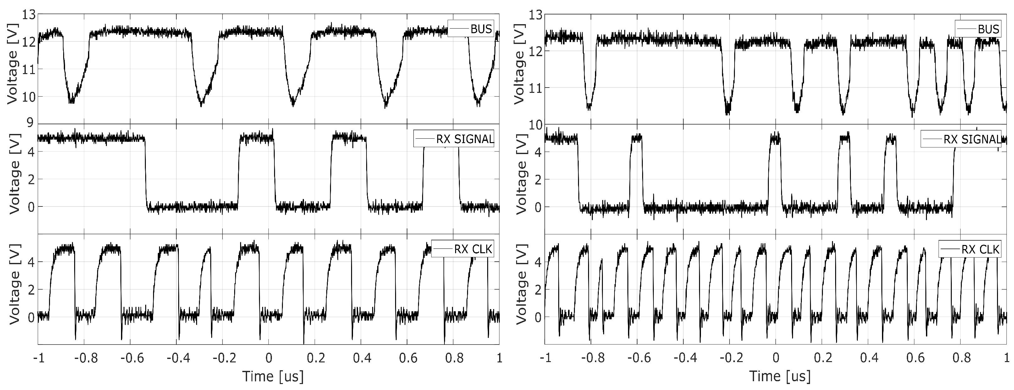
making it possible to complete a state ( that can be assumed as reference time to complete a charge or discharge phase) in 500 ns and therefore to reach a data rate of 2 Mbps with both of the proposed solutions. The Transmission Bus at Demonstrator node received data and clock are shown in Figure 12 for the H-Bridge and the 3-Switches topologies in case = 6 m and = 0.25 m are applied. As a data source, a 2 Mbps pseudo-random bit stream (PRBS) generator is implemented in the FPGA according to Table 1 and Table 2. Pulse amplitude and timing constants for three different tested combinations of and are reported in Table 3 and Table 4. Furthermore, tests with smaller capacitances have been carried out to reach data rates of up to 10 Mbps. Measurement results at 5 Mbps and 10 Mbps are shown in Figure 13 for the H-Bridge TX, and data are reported in Table 3 and Table 4 as well. The peaks amplitude in the 3-Switches implementation are lower than in the H-Bridge as expected by comparing Equation (2) in the different circuits and phases.
6. Conclusions
A PowerLine-Communication method based on direct modulation for the automotive environment is presented in this paper. Two Switching Capacitors’ transmission circuits are analyzed, and a Test Chip has been implemented in HV-CMOS SOI 180 nm technology to validate the proposal. Communication tests with a discrete component receiver board show that a data rate of 2 Mbps is reachable even using 6 m of wiring in the between. Moreover, results show that this method can potentially reach a data rate of up to 10 Mbps still offering pulses amplitude of 500 mV. The implementation allows low latencies in the applied communication, making it able to implement high-speed, time-triggered, and event-driven automotive networks.
Author Contributions
Writing—original draft, F.D.; writing—review and editing, F.D., A.O. and A.B.; investigation, A.O., F.D. and A.B.; methodology, A.O.; project administration, A.B.; supervision, A.B.; validation, F.D. and A.O.; formal analysis, F.D. All authors have read and agreed to the published version of the manuscript.
Funding
This research received no external funding.
Data Availability Statement
Please contact the Corresponding author.
Conflicts of Interest
The authors declare no conflict of interest.
References
- Ahmad, A. Automotive Semiconductor Industry—Trends, Safety and Security Challenges. In Proceedings of the 2020 8th International Conference on Reliability, Infocom Technologies and Optimization (Trends and Future Directions) (ICRITO), Noida, India, 4–5 June 2020; pp. 1373–1377. [Google Scholar]
- Challenges and Technologies—NXP Semiconductor. Available online: https://www.nxp.com/files-static/training_pdf/VFTF09_AA106.pdf (accessed on 19 July 2022).
- Heisler, P.; Kuhn, M.; Süß-Wolf, R.; Franke, J. Innovative Solutions for the Covering Process in the Manufacturing of Wire Harnesses to Increase the Automation Degree. In Proceedings of the 2020 IEEE 11th International Conference on Mechanical and Intelligent Manufacturing Technologies (ICMIMT), Cape town, South Africa, 20–22 January 2020; pp. 193–201. [Google Scholar]
- Lodi, G.A.; Ott, A.; Cheema, S.A.; Haardt, M.; Freitag, T. Power Line Communication in automotive harness on the example of Local Interconnect Network. In Proceedings of the International Symposium on Power Line Communications and its Applications, (ISPLC), Bottrop, Germany, 20–23 May 2016. [Google Scholar]
- DCAN500 CAN Power Line Transceiver. Available online: https://yamar.com/product/dcan500/ (accessed on 19 July 2022).
- Llaria, A.; Terrasson, G.; Pierlot, N. Feasibility of power supply over CAN bus: Study on different elementary design aspects. In Proceedings of the 2018 IEEE/AIAA 37th Digital Avionics Systems Conference (DASC), London, UK, 23–27 September 2018; pp. 1–7. [Google Scholar]
- ISO/TX 22/SC 31; ISO 11898-2:2016: Road Vehicles—Controller Area Network (CAN)—Part 2: High-Speed Medium Access Unit. ISO: Geneva, Switzerland, 2016.
- Grassi, F.; Pignari, S.A. Coupling/decoupling circuits for powerline communications in differential DC power buses. In Proceedings of the 2012 IEEE International Symposium on Power Line Communications and Its Applications, ISPLC 2012, Beijing, China, 27–30 March 2012; pp. 392–397. [Google Scholar]
- D’Aniello, F.; Ott, A.; Baschirotto, A. Supply Line Embedded Communication inAutomotive Sensor/Actuator Networks. In Proceedings of the 2021 IEEE International Symposium on Circuits and Systems, ISCAS 2021, Daegu, Korea, 23–26 May 2021. [Google Scholar]
- Ott, A.; D’Aniello, F.; Baschirotto, A. A Switched Capacitor Approach for Power Line Communication in Differential Networks. In Proceedings of the 2022 IEEE 17th International Conference on PhD Research in Microelectronics and Electronics, PRIME 2022, Villasimius, Italy, 12–15 June 2022. [Google Scholar]
- ISO/TC 22/SC 31; ISO 17987-3:2016: Road Vehicles—Local Inter-Connect Network (LIN)—Part 3: Protocol Specification. ISO: Geneva, Switzerland, 2016.
- Deffebach, H.L.; Frost, W. A Survey of Digital Baseband Signaling Techniques. NASA George C. Marshall Space Flight Center, Alabama, Tech. Rep. 1971. Available online: https://ntrs.nasa.gov/api/citations/19710028227/downloads/19710028227.pdf (accessed on 19 July 2022).
- D’Aniello, F.; Ott, A.; Baschirotto, A. StrongArm-Latch-Based Receiver for Supply Line Embedded Communication. In Proceedings of the 2022 IEEE 17th International Conference on PhD Research in Microelectronics and Electronics, PRIME 2022, Villasimius, Italy, 12–15 June 2022. [Google Scholar]
Figure 1.
Equivalent s-domain model of the charge injection.

Figure 2.
Simulation results of a discharge event.
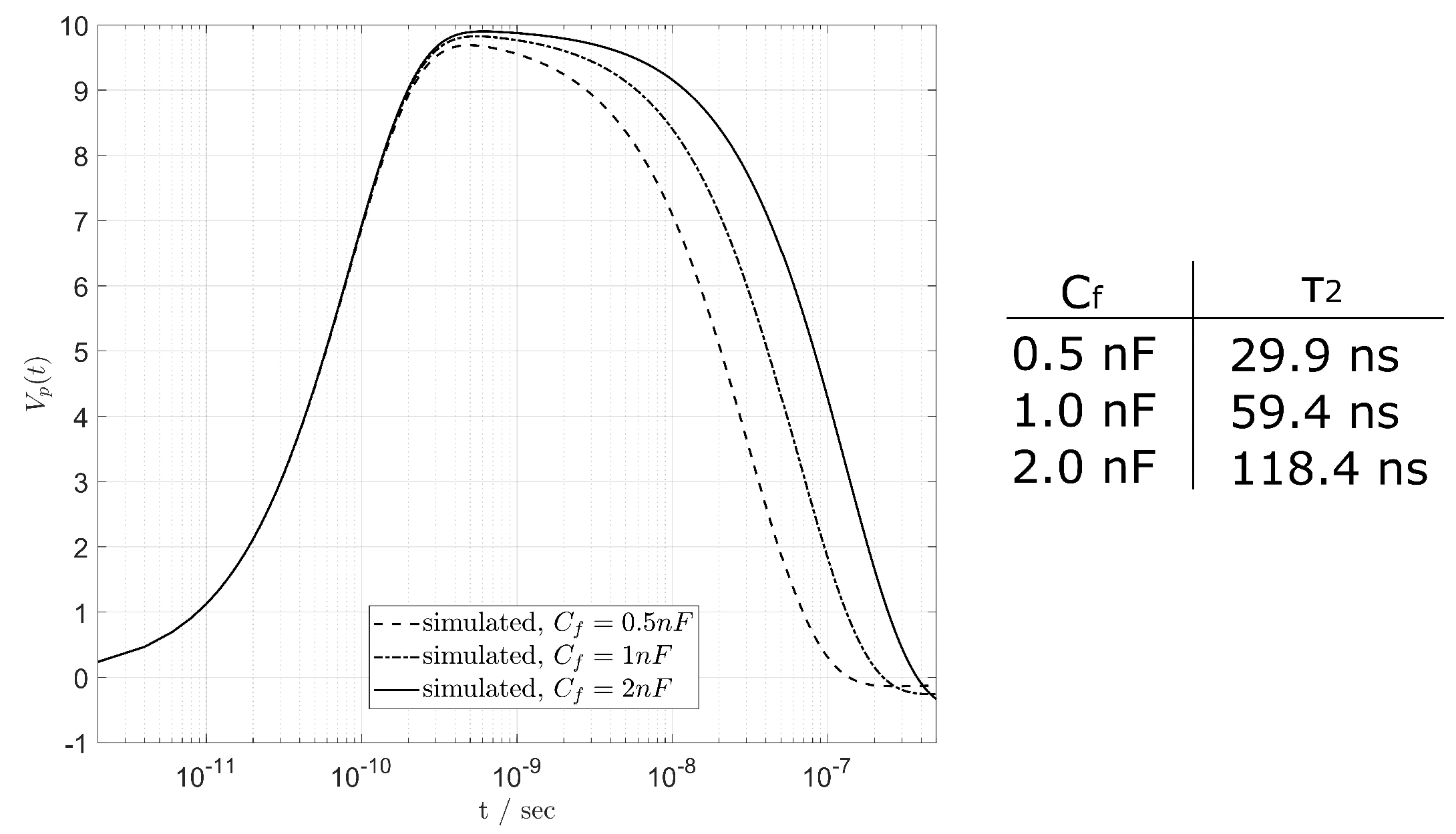
Figure 3.
H-Bridge TX topology.
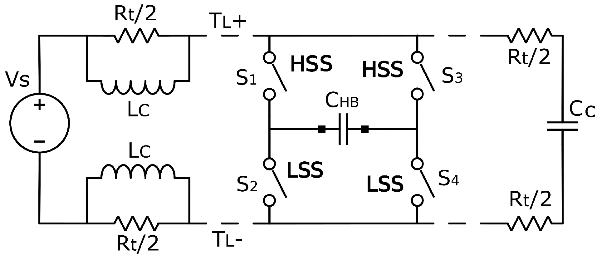
Figure 4.
Example of transmission in H-Bridge TX topology.

Figure 5.
3-switches TX topology.
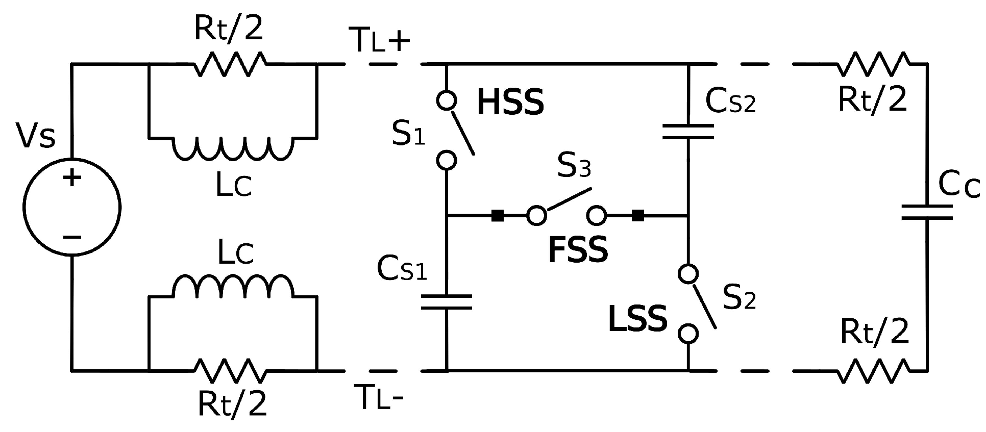
Figure 6.
Example of transmission in the 3-switches TX topology.

Figure 7.
FS schematic.
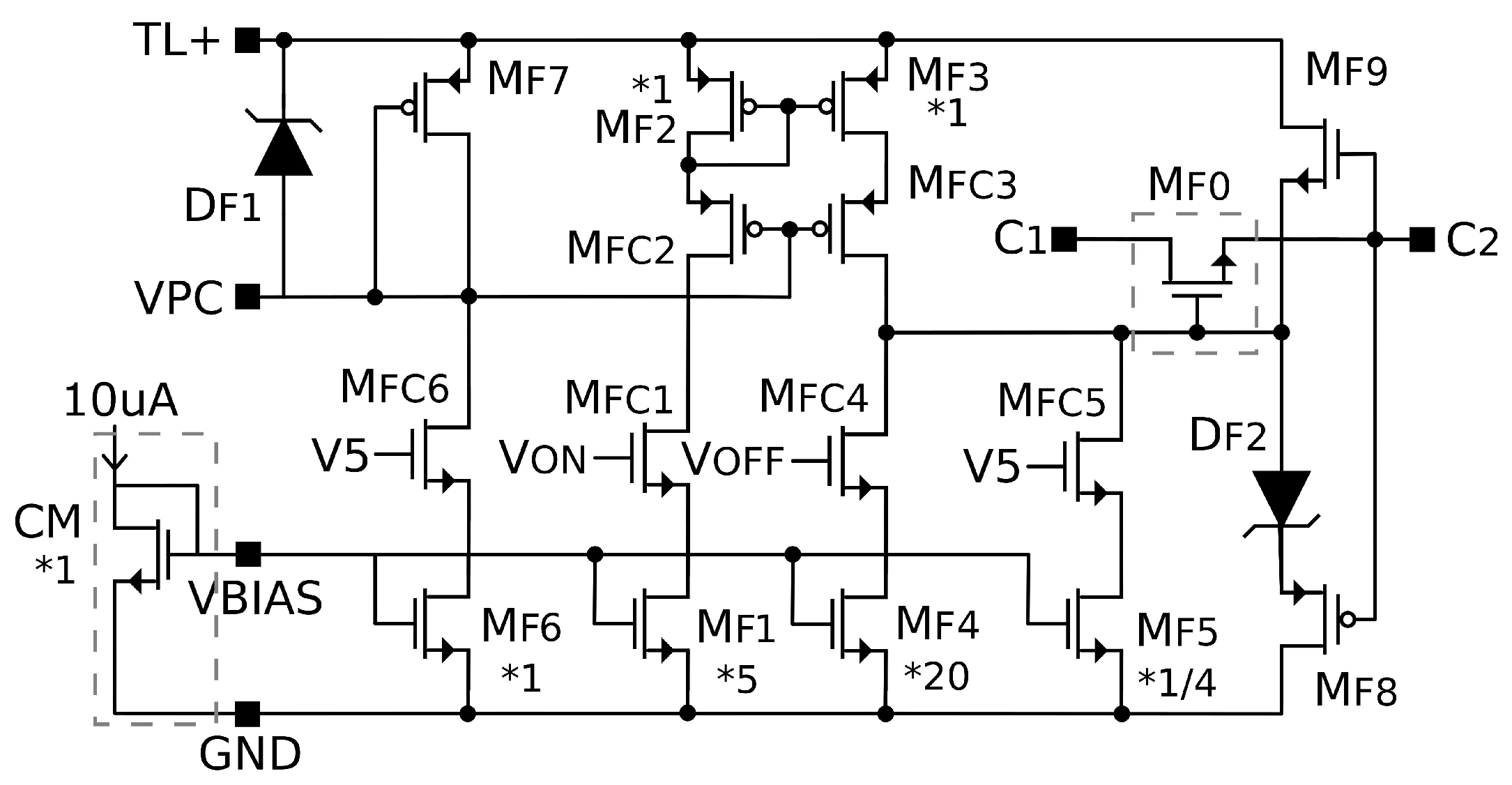
Figure 8.
LSS schematic.

Figure 9.
HSS schematic.
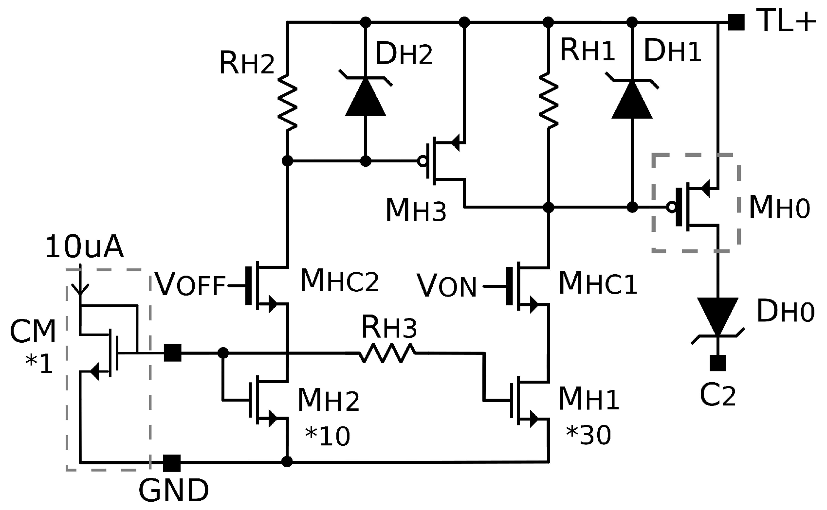
Figure 10.
Test Chip 2000× micrographs picture.
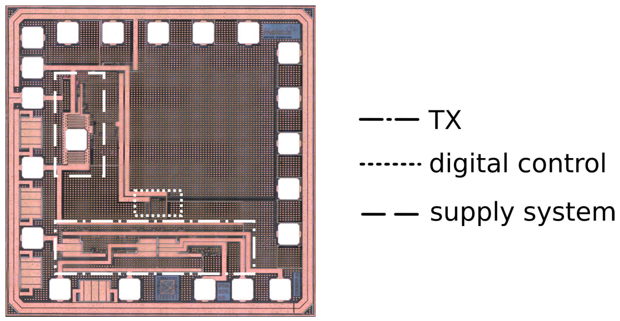
Figure 11.
Measurement setup.
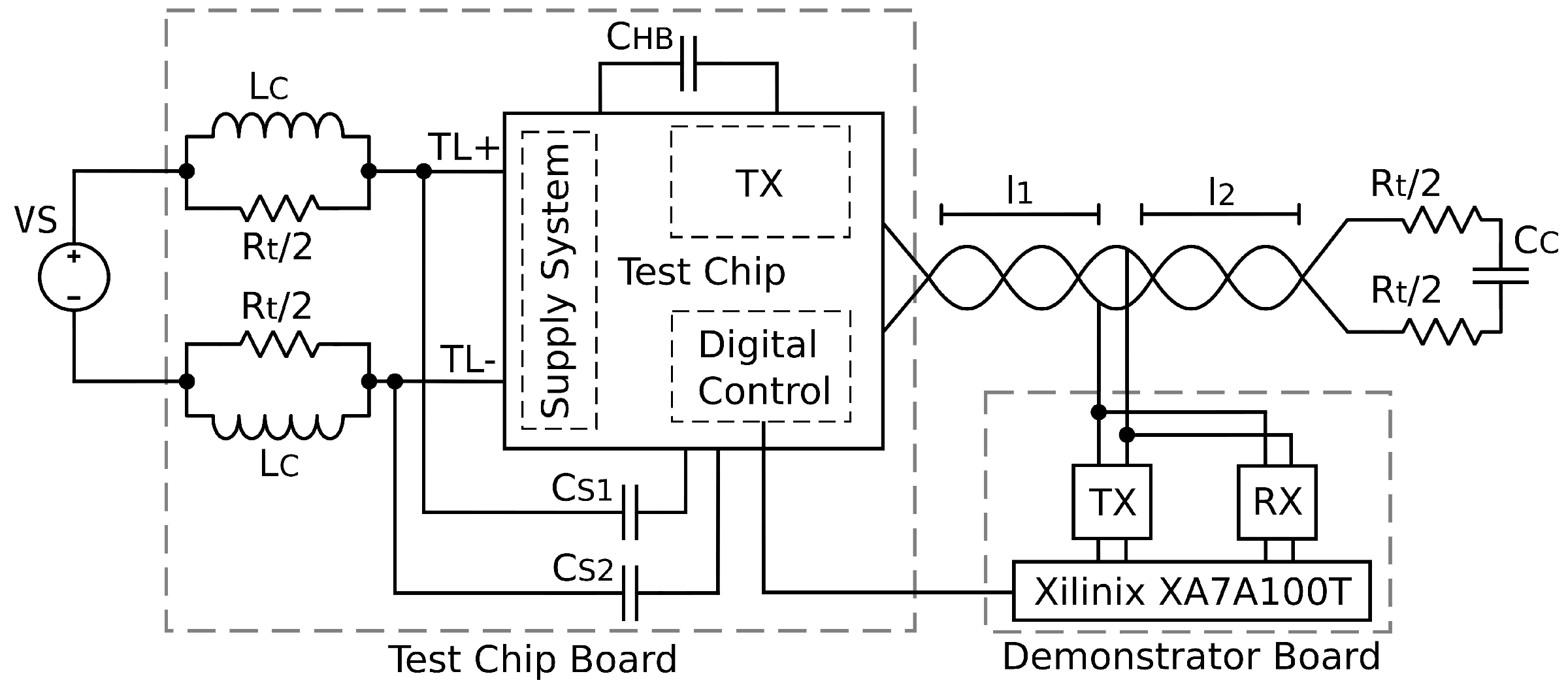
Figure 12.
Transmission Bus, received data and received clock at 2 Mbps (switching capacitors = 820 pF) for the 3-Switches (left) and the H-Bridge (right) transmitters.
Figure 12.
Transmission Bus, received data and received clock at 2 Mbps (switching capacitors = 820 pF) for the 3-Switches (left) and the H-Bridge (right) transmitters.
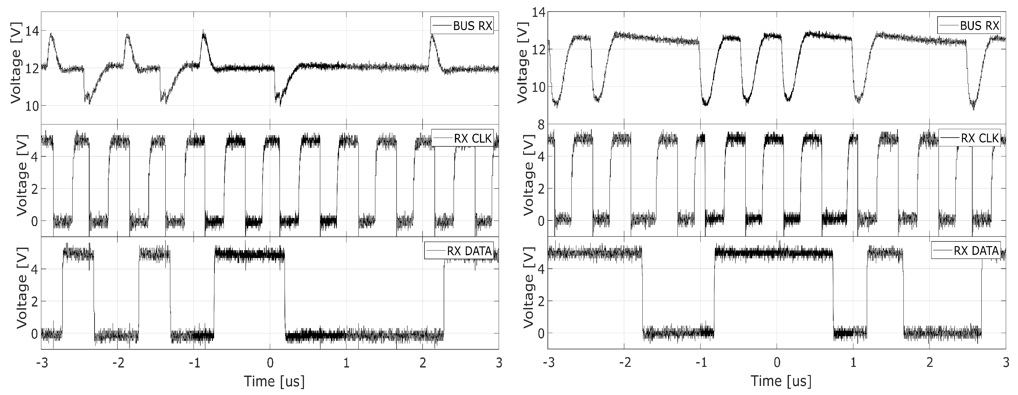
Figure 13.
Transmission Bus, received data and received clock at 5 Mbps (switching capacitors = 330 pF) and 10 Mbps (switching capacitors = 180 pF) for the H-Bridge transmitter.
Figure 13.
Transmission Bus, received data and received clock at 5 Mbps (switching capacitors = 330 pF) and 10 Mbps (switching capacitors = 180 pF) for the H-Bridge transmitter.

Table 1.
States of H-Bridge transmitter topology.
| State | S1, S4 | S2, S3 | Description |
|---|---|---|---|
| Open | Open | Open | not connected. Charge is preserved |
| Charge 1–4 | Close | Open | charge accumulated during Charge 2–3 phase is recharged to level |
| Charge 2–3 | Open | Close | charge accumulated during Charge 1–4 phase is recharged to the level |
Table 2.
States of 3-switches transmitter topology.
| State | S1, S2 | S3 | Description |
|---|---|---|---|
| Open | Open | Open | , not connected. Charges are preserved |
| Charge | Close | Open | , are connected in parallel to the bus and charged to |
| Discharge | Open | Close | , are connected in series and discharged to |
Table 3.
Measurement results for the H-Bridge TX.
| l1 = 0.25 m l2 = 0.25 m | l1 = 6 m l2 = 0.25 m | l1 = 0.25 m l2 = 6 m | ||||
|---|---|---|---|---|---|---|
| Charge 1–4/2–3 | Charge 1–4/2–3 | Charge 1–4/2–3 | ||||
| 820 pF | 3.29 | 240 | 2.85 | 251 | 4.35 | 246 |
| 330 pF | 3.16 | 120 | 2.6 | 124 | 4.04 | 125 |
| 180 pF | 2.75 | 81 | 2.19 | 91 | 3.14 | 83 |
Table 4.
Measurement result for the 3-Switches TX.
| l1 = 0.25 m l2 = 0.25 m | l1 = 6 m l2 = 0.25 m | l1 = 0.25 m l2 = 6 m | ||||||||||
|---|---|---|---|---|---|---|---|---|---|---|---|---|
| Charge | Discharge | Charge | Discharge | Charge | Discharge | |||||||
| 820 pF | 2.88 | 211 | 2.5 | 96 | 2.13 | 254 | 1.81 | 95 | 3.38 | 203 | 2.81 | 94 |
| 330 pF | 2.63 | 97 | 1.31 | 72 | 1.59 | 140 | 1.03 | 72 | 2.88 | 114 | 1.56 | 70 |
| 180 pF | 2.16 | 55 | 0.78 | 65 | 1.44 | 96 | 0.59 | 59 | 2.44 | 78 | 0.97 | 60 |
Publisher’s Note: MDPI stays neutral with regard to jurisdictional claims in published maps and institutional affiliations. |
© 2022 by the authors. Licensee MDPI, Basel, Switzerland. This article is an open access article distributed under the terms and conditions of the Creative Commons Attribution (CC BY) license (https://creativecommons.org/licenses/by/4.0/).
Share and Cite
MDPI and ACS Style
D’Aniello, F.; Ott, A.; Baschirotto, A. 2-Mbps Power-Line Communication Transmitter Based on Switched Capacitors for Automotive Networks. Electronics 2022, 11, 3651. https://doi.org/10.3390/electronics11223651
AMA Style
D’Aniello F, Ott A, Baschirotto A. 2-Mbps Power-Line Communication Transmitter Based on Switched Capacitors for Automotive Networks. Electronics. 2022; 11(22):3651. https://doi.org/10.3390/electronics11223651
Chicago/Turabian StyleD’Aniello, Federico, Andreas Ott, and Andrea Baschirotto. 2022. "2-Mbps Power-Line Communication Transmitter Based on Switched Capacitors for Automotive Networks" Electronics 11, no. 22: 3651. https://doi.org/10.3390/electronics11223651
Note that from the first issue of 2016, this journal uses article numbers instead of page numbers. See further details here.