
A Differential-to-Single-Ended Converter Based on Enhanced Body-Driven Current Mirrors Targeting Ultra-Low-Voltage OTAs
 ,
,  , ,
, ,
Abstract
:1. Introduction
2. Proposed Topology of Enhanced Body-Driven Current Mirror
2.1. Comparison between the Conventional Body-Driven Current Mirror and the Proposed Improved One
- The value of , which can be minimized if is much lower than ;
- The matching between and .
- The value of , which can be minimized by increasing for a given value of and ;
- The matching between and .
2.2. The Error Amplifier
3. Conventional and Enhanced D2S Circuits
3.1. Conventional D2S Converter Based on Body-Driven Current Mirrors
3.2. D2S Converter Based on Enhanced BD-CM
4. Two-Stage OTA Based on the Proposed Enhanced D2S
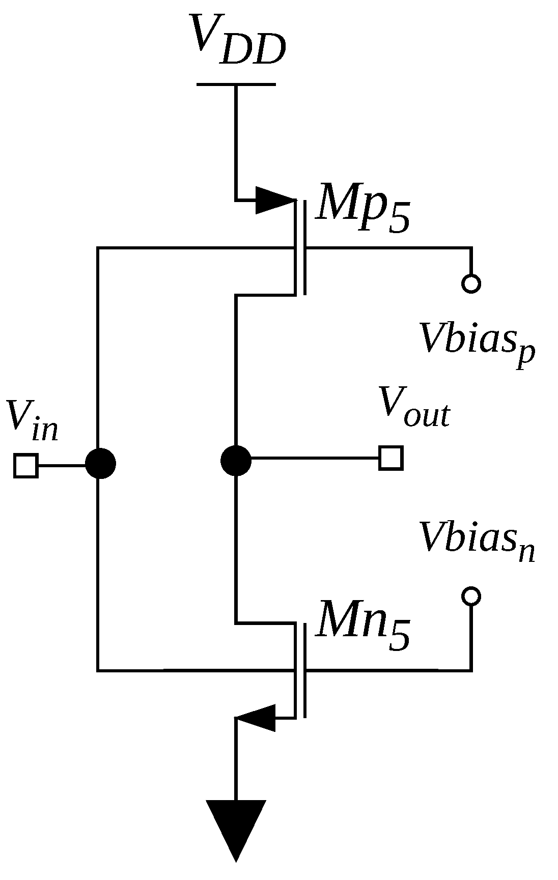
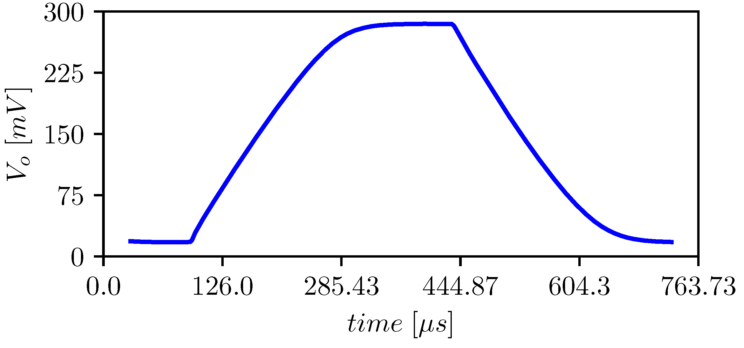
4.1. Output Stage
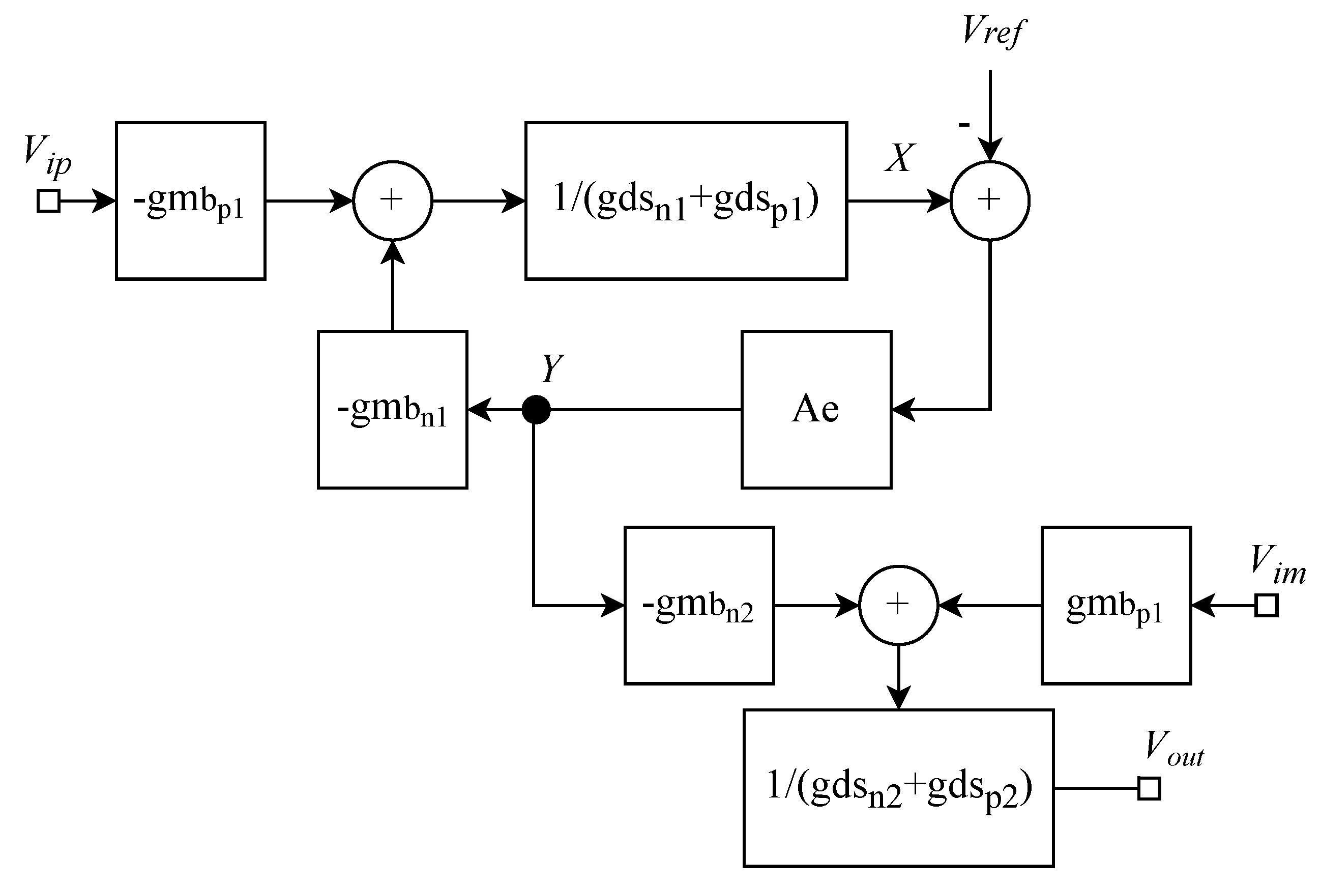
4.2. Analysis of the Proposed ULV OTA
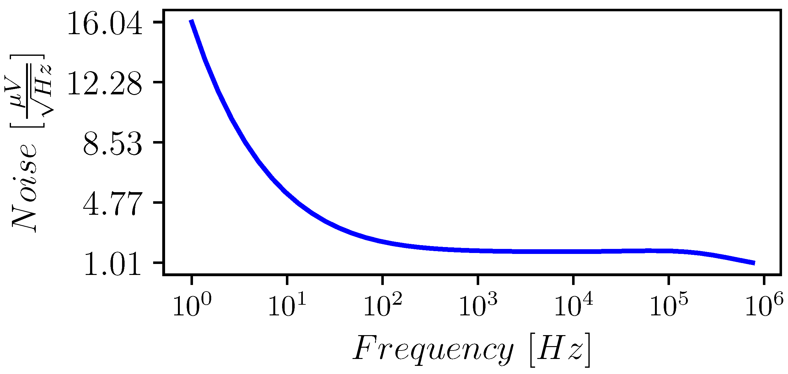
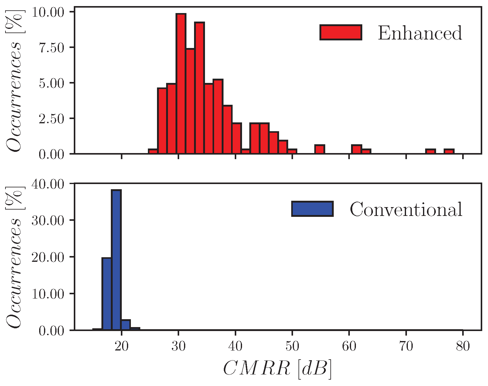
5. Simulation Results
OTA Performance and Characterization
6. Comparison
7. Conclusions
Author Contributions
Funding
Conflicts of Interest
Abbreviations
| ULV | Ultra-Low Voltage |
| ULP | Ultra-Low Power |
| D2S | Differential to Single Ended |
| PSRR | Power Supply Rejection Ratio |
| CMRR | Common-Mode Rejection Ratio |
| OTA | Operational Transconductance Amplifier |
| IoT | Internet of Things |
| FOM | Figure of Merit |
| FDSOI | Fully Depleted Silicon on Insulator |
| BD | Body Driven |
| BD-CM | Body-Driven Current Mirror |
| GD | Gate Driven |
| PVT | Process Voltage and Temperature |
| DIG | Digital |
| IRN | Input-Referred Noise |
| THD | Total Harmonic Distortion |
| Pd | Power Dissipation |
| SR | Slew Rate |
References
- Lee, J.; Johnson, M.; Kipke, D. A tunable biquad switched-capacitor amplifier-filter for neural recording. IEEE Trans. Biomed. Circuits Syst. 2010, 4, 295–300. [Google Scholar] [CrossRef] [PubMed]
- Della Sala, R.; Monsurrò, P.; Scotti, G.; Trifiletti, A. Area-efficient low-power bandpass Gm-C filter for epileptic seizure detection in 130 nm CMOS. In Proceedings of the 2019 26th IEEE International Conference on Electronics, Circuits and Systems (ICECS), Genoa, Italy, 27–29 November 2019; IEEE: Genoa, Italy, 2019; pp. 298–301. [Google Scholar] [CrossRef]
- Liu, Z.; Tan, Y.; Li, H.; Jiang, H.; Liu, J.; Liao, H. A 0.5-V 3.69-nW complementary source-follower-C based low-pass filter for wearable biomedical applications. IEEE Trans. Circ. Syst. I 2020, 67, 4370–4381. [Google Scholar] [CrossRef]
- Sanchotene Silva, R.; Rodovalho, L.H.; Aiello, O.; Ramos Rodrigues, C. A 1.9 nW, sub-1 V, 542 pA/V linear bulk-driven OTA with 154 dB CMRR for bio-sensing applications. J. Low Power Electron. Appl. 2021, 11, 40. [Google Scholar] [CrossRef]
- Della Sala, R.; Centurelli, F.; Monsurrò, P.; Scotti, G. Sub-μW front-end low noise amplifier for neural recording applications. In Proceedings of the 2022 17th Conference on Ph.D Research in Microelectronics and Electronics (PRIME), Villasimius, Italy, 12–15 June 2022; IEEE: Villasimius, Italy, 2022; pp. 305–308. [Google Scholar] [CrossRef]
- Harpe, P.; Gao, H.; van Dommele, R.; Cantatore, E.; van Roermund, A.H.M. A 0.20 mm2 3 nW signal acquisition IC for miniature sensor nodes in 65 nm CMOS. IEEE J. Solid-State Circuits 2016, 51, 240–248. [Google Scholar] [CrossRef]
- Harikumar, P.; Wikner, J.J.; Alvandpour, A. A 0.4-V subnanowatt 8-bit 1-kS/s SAR ADC in 65-nm CMOS for wireless sensor applications. IEEE Trans. Circuits Syst. II 2016, 63, 743–747. [Google Scholar] [CrossRef]
- Wu, T.; Wu, F.; Redouté, J.M.; Yuce, M.R. An autonomous wireless body area network implementation towards IoT connected healthcare applications. IEEE Access 2017, 5, 11413–11422. [Google Scholar] [CrossRef]
- Pu, X.; An, S.; Tang, Q.; Guo, H.; Hu, C. Wearable triboelectric sensors for biomedical monitoring and human-machine interface. iScience 2021, 24, 102027. [Google Scholar] [CrossRef]
- Alioto, M.; Shahghasemi, M. The Internet of Things on its edge: Trends toward its tipping point. IEEE Consum. Electron. Mag. 2017, 7, 77–87. [Google Scholar] [CrossRef]
- Aiello, O.; Crovetti, P.; Alioto, M. Ultra-low power and minimal design effort interfaces for the Internet of Things. In Proceedings of the 2019 IEEE International Circuits and Systems Symposium (ICSyS), Kuantan, Pahang, Malaysia, 18–19 September 2019; IEEE: Kuantan, Pahang, Malaysia, 2019; pp. 1–4. [Google Scholar] [CrossRef]
- Sobin, C.C. A survey on architecture, protocols and challenges in IoT. Wirel. Pers. Commun. 2020, 112, 1383–1429. [Google Scholar] [CrossRef]
- Grossi, M. Energy harvesting strategies for wireless sensor networks and mobile devices: A review. Electronics 2021, 10, 661. [Google Scholar] [CrossRef]
- Khateb, F.; Dabbous, S.B.A.; Vlassis, S. A survey of non-conventional techniques for low-voltage low-power analog circuit design. Radioengineering 2013, 22, 415–427. [Google Scholar]
- Grasso, A.D.; Pennisi, S. Ultra-low power amplifiers for IoT nodes. In Proceedings of the 2018 25th IEEE International Conference on Electronics, Circuits and Systems (ICECS), Bordeaux, France, 9–12 December 2018; IEEE: Bordeaux, France, 2018; pp. 497–500. [Google Scholar] [CrossRef]
- Toledo, P.; Rubino, R.; Musolino, F.; Crovetti, P. Re-thinking analog integrated circuits in digital terms: A new design concept for the IoT era. IEEE Trans. Circuits Syst. II 2021, 68, 816–822. [Google Scholar] [CrossRef]
- Giustolisi, G.; Palumbo, G. A gm/ID-Based Design Strategy for IoT and Ultra-Low-Power OTAs with Fast-Settling and Large Capacitive Loads. J. Low Power Electron. Appl. 2021, 11, 21. [Google Scholar] [CrossRef]
- Richelli, A.; Colalongo, L.; Kovacs-Vajna, Z.; Calvetti, G.; Ferrari, D.; Finanzini, M.; Pinetti, S.; Prevosti, E.; Savoldelli, J.; Scarlassara, S. A survey of low voltage and low power amplifier topologies. J. Low Power Electron. Appl. 2018, 8, 22. [Google Scholar] [CrossRef] [Green Version]
- Centurelli, F.; Della Sala, R.; Monsurrò, P.; Scotti, G.; Trifiletti, A. A tree-based architecture for high-performance ultra-low-voltage amplifiers. J. Low Power Electron. Appl. 2022, 12, 12. [Google Scholar] [CrossRef]
- Della Sala, R.; Centurelli, F.; Scotti, G. Enabling ULV fully synthesizable analog circuits: The BA cell, a standard-cell-based building block for analog design. IEEE Trans. Circuits Syst. II 2022, 1. [Google Scholar] [CrossRef]
- Mastrandrea, A.; Menichelli, F.; Olivieri, M. A delay model allowing nano-CMOS standard cells statistical simulation at the logic level. In Proceedings of the 2011 7th Conference on Ph.D. Research in Microelectronics and Electronics, Madonna di Campiglio, Italy, 3–7 July 2011; IEEE: Madonna di Campiglio, Italy, 2011; pp. 217–220. [Google Scholar] [CrossRef]
- Khalid, U.; Mastrandrea, A.; Olivieri, M. Novel approaches to quantify failure probability due to process variations in nano-scale CMOS logic. In Proceedings of the 2014 29th International Conference on Microelectronics Proceedings—MIEL 2014, Belgrade, Serbia, 12–14 May 2014; IEEE: Belgrade, Serbia, 2014; pp. 371–374. [Google Scholar] [CrossRef]
- Abdelfattah, O.; Roberts, G.W.; Shih, I.; Shih, Y.C. An ultra-low-voltage CMOS process-insensitive self-biased OTA with rail-to-rail input range. IEEE Trans. Circ. Syst. I 2015, 62, 2380–2390. [Google Scholar] [CrossRef]
- Baghtash, H.F. A 0.4 V, body-driven, fully differential, tail-less OTA based on current push-pull. Microelectron. J. 2020, 99, 104768. [Google Scholar] [CrossRef]
- Della Sala, R.; Centurelli, F.; Monsurrò, P.; Scotti, G. High-efficiency 0.3V OTA in CMOS 130nm technology using current mirrors with gain. In Proceedings of the 2022 17th Conference on Ph.D Research in Microelectronics and Electronics (PRIME), Villasimius, SU, Italy, 12–15 June 2022; IEEE: Villasimius, SU, Italy, 2022; pp. 69–72. [Google Scholar] [CrossRef]
- Ng, K.A.; Xu, Y.P. A low-power, high CMRR neural amplifier system employing CMOS inverter-based OTAs with CMFB through supply rails. IEEE J. Solid-State Circuits 2016, 51, 724–737. [Google Scholar] [CrossRef]
- Crovetti, P.S. A digital-based analog differential circuit. IEEE Trans. Circ. Syst. I 2013, 60, 3107–3116. [Google Scholar] [CrossRef]
- Toledo, P.; Crovetti, P.; Aiello, O.; Alioto, M. Design of digital OTAs with operation down to 0.3 V and nW power for direct harvesting. IEEE Trans. Circ. Syst. I 2021, 68, 3693–3706. [Google Scholar] [CrossRef]
- Palumbo, G.; Scotti, G. A Novel Standard-Cell-Based Implementation of the Digital OTA Suitable for Automatic Place and Route. J. Low Power Electron. Appl. 2021, 11, 42. [Google Scholar] [CrossRef]
- Braga, R.A.S.; Ferreira, L.H.C.; Coletta, G.D.; Dutra, O.O. A 0.25-V calibration-less inverter-based OTA for low-frequency Gm-C applications. Microelectron. J. 2019, 83, 62–72. [Google Scholar] [CrossRef]
- Lv, L.; Zhou, X.; Qiao, Z.; Li, Q. Inverter-based subthreshold amplifier techniques and their application in 0.3-V ΔΣ -Modulators. IEEE J. Solid-State Circuits 2019, 54, 1436–1445. [Google Scholar] [CrossRef]
- Manfredini, G.; Catania, A.; Benvenuti, L.; Cicalini, M.; Piotto, M.; Bruschi, P. Ultra-low-voltage inverter-based amplifier with novel common-mode stabilization loop. Electronics 2020, 9, 1019. [Google Scholar] [CrossRef]
- Rodovalho, L.H.; Aiello, O.; Rodrigues, C.R. Ultra-low-voltage inverter-based operational transconductance amplifiers with voltage gain enhancement by improved composite transistors. Electronics 2020, 9, 1410. [Google Scholar] [CrossRef]
- Póvoa, R.; Canelas, A.; Martins, R.; Horta, N.; Lourenço, N.; Goes, J. A new family of CMOS inverter-based OTAs for biomedical and healthcare applications. Integration 2020, 71, 38–48. [Google Scholar] [CrossRef]
- Rodovalho, L.H.; Ramos Rodrigues, C.; Aiello, O. Self-biased and supply-voltage scalable inverter-based operational transconductance amplifier with improved composite transistors. Electronics 2021, 10, 935. [Google Scholar] [CrossRef]
- Centurelli, F.; Della Sala, R.; Scotti, G. A standard-cell-based CMFB for fully synthesizable OTAs. J. Low Power Electron. Appl. 2022, 12, 27. [Google Scholar] [CrossRef]
- Della Sala, R.; Centurelli, F.; Scotti, G. A novel differential to single-ended converter for ultra-low-voltage inverter-based OTAs. IEEE Access 2022, 10, 98179–98190. [Google Scholar] [CrossRef]
- Miguel, J.M.A.; Lopez-Martin, A.J.; Acosta, L.; Ramirez-Angulo, J.; Carvajal, R.G. Using floating gate and quasi-floating gate techniques for rail-to-rail tunable CMOS transconductor design. IEEE Trans. Circ. Syst. I 2011, 58, 1604–1614. [Google Scholar] [CrossRef]
- Khateb, F. Bulk-driven floating-gate and bulk-driven quasi-floating-gate techniques for low-voltage low-power analog circuits design. AEU Int. J. Electron. Commun. 2014, 68, 64–72. [Google Scholar] [CrossRef]
- Khateb, F.; Kulej, T.; Veldandi, H.; Jaikla, W. Multiple-input bulk-driven quasi-floating-gate MOS transistor for low-voltage low-power integrated circuits. AEU Int. J. Electron. Commun. 2019, 100, 32–38. [Google Scholar] [CrossRef]
- Ferreira, L.H.C.; Sonkusale, S.R. A 60-dB gain OTA operating at 0.25-V power supply in 130-nm digital CMOS process. IEEE Trans. Circ. Syst. I 2014, 61, 1609–1617. [Google Scholar] [CrossRef]
- Akbari, M.; Hashemipour, O. A 63-dB gain OTA operating in subthreshold with 20-nW power consumption. Int. J. Circuit Theory Appl. 2017, 45, 843–850. [Google Scholar] [CrossRef]
- Kulej, T.; Khateb, F. Design and implementation of sub 0.5-V OTAs in 0.18-μm CMOS. Int. J. Circuit Theory Appl. 2018, 46, 1129–1143. [Google Scholar] [CrossRef]
- Veldandi, H.; Shaik, R.A. A 0.3-V pseudo-differential bulk-input OTA for low-frequency applications. Circuits Syst. Signal Process. 2018, 37, 5199–5221. [Google Scholar] [CrossRef]
- Kulej, T.; Khateb, F. A compact 0.3-V class AB bulk-driven OTA. IEEE Trans. Very Large Scale Integr. VLSI Syst. 2020, 28, 224–232. [Google Scholar] [CrossRef]
- Kulej, T.; Khateb, F. A 0.3-V 98-dB rail-to-rail OTA in 0.18 μm CMOS. IEEE Access 2020, 8, 27459–27467. [Google Scholar] [CrossRef]
- Woo, K.C.; Yang, B.D. A 0.25-V rail-to-rail three-stage OTA with an enhanced DC gain. IEEE Trans. Circuits Syst. II 2020, 67, 1179–1183. [Google Scholar] [CrossRef]
- Fortes, A.; Quirino, F.A.; da Silva, L.A.; Girardi, A. Low power bulk-driven OTA design optimization using cuckoo search algorithm. Analog Integr. Circ. Sig. Process. 2021, 106, 99–109. [Google Scholar] [CrossRef]
- Wang, Y.; Zhang, Q.; Zhao, X.; Dong, L. An enhanced bulk-driven OTA with high transconductance against CMOS scaling. AEU Int. J. Electron. Commun. 2021, 130, 153581. [Google Scholar] [CrossRef]
- Centurelli, F.; Della Sala, R.; Scotti, G.; Trifiletti, A. A 0.3 V, rail-to-rail, ultralow-power, non-tailed, body-driven, sub-threshold amplifier. Appl. Sci. 2021, 11, 2528. [Google Scholar] [CrossRef]
- Centurelli, F.; Della Sala, R.; Monsurrò, P.; Scotti, G.; Trifiletti, A. A 0.3 V rail-to-rail ultra-low-power OTA with improved bBandwidth and slew rate. J. Low Power Electron. Appl. 2021, 11, 19. [Google Scholar] [CrossRef]
- Ghosh, S.; Bhadauria, V. High current efficiency single-stage bulk-driven subthreshold-biased class-AB OTAs with enhanced transconductance and slew rate for large capacitive loads. Analog Integr. Circuits Signal Process. 2021, 109, 403–433. [Google Scholar] [CrossRef]
- Kulej, T.; Khateb, F.; Arbet, D.; Stopjakova, V. A 0.3-V High Linear Rail-to-Rail Bulk-Driven OTA in 0.13 μm CMOS. IEEE Trans. Circuits Syst. II 2022, 69, 2046–2050. [Google Scholar] [CrossRef]
- Dong, S.; Wang, W.; Tong, X. A 0.25-V 90 dB PVT-stabilized four-stage OTA with linear Q-factor modulation and fast slew-rate enhancement for ultra-low supply ADCs. AEU Int. J. Electron. Commun. 2022, 144, 154044. [Google Scholar] [CrossRef]
- Centurelli, F.; Della Sala, R.; Monsurró, P.; Tommasino, P.; Trifiletti, A. An ultra-low-voltage class-AB OTA exploiting local CMFB and body-to-gate interface. AEU Int. J. Electron. Commun. 2022, 145, 154081. [Google Scholar] [CrossRef]
- Castaño, F.; Torelli, G.; Pérez-Aloe, R.; Carrillo, J.M. Low-voltage rail-to-rail bulk-driven CMFB network with improved gain and bandwidth. In Proceedings of the 2010 17th IEEE International Conference on Electronics, Circuits and Systems, Athens, Greece, 12–15 December 2010; IEEE: Athens, Greece, 2010; pp. 207–210. [Google Scholar] [CrossRef]
- Rajendran, S.; Chakrapani, A.; Kannan, S.; Ansari, A.Q. A research perspective on CMOS current mirror circuits: Configurations and techniques. Recent Adv. Electr. Electron. Eng. (Former. Recent Patents Electr. Electron. Eng. 2021, 14, 377–397. [Google Scholar] [CrossRef]
- Toledo, P.; Crovetti, P.; Aiello, O.; Alioto, M. Fully digital rail-to-rail OTA with sub-1000-μm2 area, 250-mV minimum supply, and nW power at 150-pF load in 180 nm. IEEE Solid-State Circuits Lett. 2020, 3, 474–477. [Google Scholar] [CrossRef]
- Toledo, P.; Crovetti, P.; Klimach, H.; Bampi, S.; Aiello, O.; Alioto, M. A 300mV-supply, sub-nW-power digital-based operational transconductance amplifier. IEEE Trans. Circuits Syst. II 2021, 68, 3073–3077. [Google Scholar] [CrossRef]
- Toledo, P.; Crovetti, P.S.; Klimach, H.D.; Musolino, F.; Bampi, S. Low-voltage, low-area, nW-power CMOS digital-based biosignal amplifier. IEEE Access 2022, 10, 44106–44115. [Google Scholar] [CrossRef]


| W (m) | L (m) | I (nA) | |
|---|---|---|---|
| 4.5 | 1.3 | 60 | |
| 48.33 | 1.3 | 60 | |
| 1.5 | 1.3 | 20 | |
| 16.11 | 1.3 | 20 | |
| 18.00 | 1.3 | 240 | |
| 193.32 | 1.3 | 240 |
| VDD (mV) | 300 | 270 | 330 | 300 | 300 |
|---|---|---|---|---|---|
| Temp. ( C) | 27 | 27 | 27 | 0 | 75 |
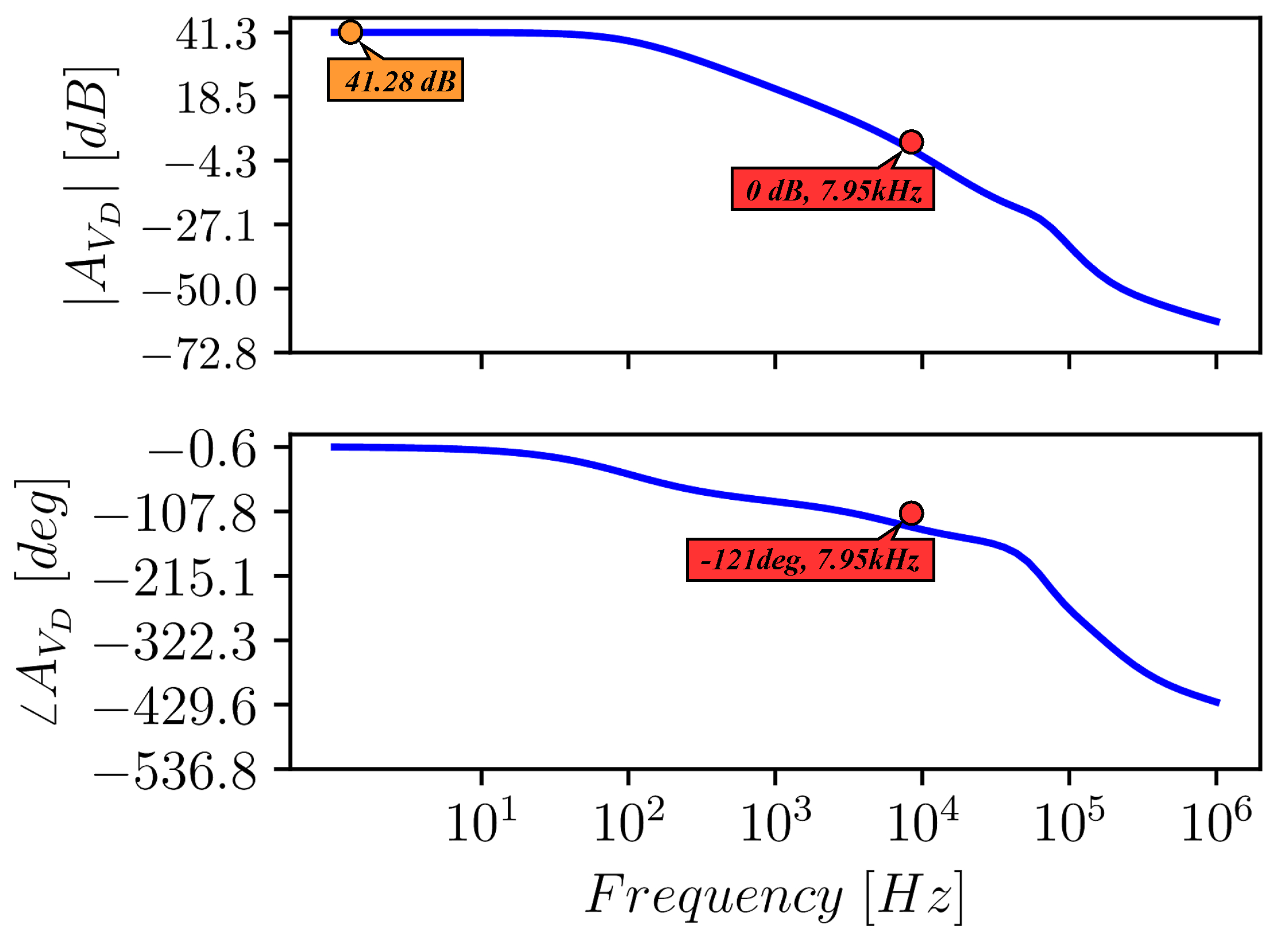
| Ad (dB) | 41.28 | 38.03 | 43.78 | 41.81 | 39.52 |
| GBW (kHz) | 7.95 | 7.48 | 8.21 | 7.12 | 8.37 |
| Phase Margin (deg) | 51 | 56.69 | 47.16 | 49.66 | 53.48 |
| Ac (dB) | 6 | 6.1 | 5.87 | 6.21 | 5.93 |
| CMRR (dB) | 35.28 | 31.93 | 37.91 | 35.60 | 33.59 |
| PSRR (dB) | 74.41 | 85.02 | 82.31 | 73.49 | 72.37 |
| Offset (V) | 2.012 | 391.3 | 182.9 | 404.7 | 962.4 |
| Pd (nW) | 120 | 107.3 | 132.7 | 119.1 | 123 |
| SR+ (V/ms) | 1.25 | 1.08 | 1.41 | 1.32 | 1.13 |
| SR- (V/ms) | 1.25 | 1.11 | 1.38 | 1.32 | 1.12 |
| THD (%) * | 3.15 | 3.23 | 4.76 | 2.85 | 3.59 |
| Corner | TYP | FF | SS | SF | FS |
|---|---|---|---|---|---|
| Ad (dB) | 41.28 | 40.34 | 42.17 | 40.82 | 41.69 |
| GBW (kHz) | 7.95 | 7.71 | 8.17 | 7.82 | 8.08 |
| Phase Margin (deg) | 51 | 53.22 | 48.13 | 52.39 | 50.12 |
| Ac (dB) | 6 | 5.84 | 6.17 | 5.23 | 6.79 |
| CMRR (dB) | 35.28 | 34.50 | 36.00 | 35.59 | 34.90 |
| PSRR (dB) | 74.41 | 77.34 | 74.97 | 78.08 | 74.95 |
| Offset (V) | 2.012 | 239.8 | 213.7 | 524 | 214 |
| Pd (nW) | 120 | 120.7 | 119.4 | 120 | 120.2 |
| SR+ (V/ms) | 1.25 | 1.21 | 1.28 | 1.24 | 1.24 |
| SR- (V/ms) | 1.25 | 1.20 | 1.30 | 1.21 | 1.29 |
| THD (%) | 3.15 | 3.23 | 3.02 | 2.34 | 2.65 |
| Conventional | Enhanced | |||
|---|---|---|---|---|
| Ad (dB) | 40.15 | 0.61 | 41.18 | 0.61 |
| GBW (kHz) | 6.94 | 0.18 | 7.93 | 0.61 |
| Phase Margin (deg) | 51.12 | 1.03 | 51 | 0.8 |
| CMRR (dB) | 17.46 | 1.1 | 35.17 | 7.25 |
| PSRR (dB) | 63.79 | 9.81 | 72.32 | 6.89 |
| Offset (mV) | 0.57 | 11.22 | 0.5 | 9.84 |
| Pd (nW) | 108 | 2.7 | 120 | 3.48 |
| SR+ (V/ms) | 1.25 | 0.11 | 1.25 | 0.11 |
| SR- (V/ms) | 1.26 | 0.04 | 1.25 | 0.05 |
| This Work * | [19] * | [55] * | [59] | [51] * | [50] * | [47] | [33] * | [46] | [45] | [31] | [43] | |
|---|---|---|---|---|---|---|---|---|---|---|---|---|
| Year | 2022 | 2022 | 2022 | 2021 | 2021 | 2021 | 2020 | 2020 | 2020 | 2020 | 2019 | 2018 |
| Tech (nm) | 130 | 130 | 130 | 180 | 130 | 130 | 65 | 180 | 180 | 180 | 130 | 180 |
| VDD (V) | 0.3 | 0.3 | 0.3 | 0.3 | 0.3 | 0.3 | 0.25 | 0.3 | 0.3 | 0.3 | 0.3 | 0.3 |
| VDD/VTH | 0.86 | 0.86 | 0.86 | 0.6 | 0.86 | 0.86 | - | 0.6 | 0.6 | 0.6 | 0.86 | 0.6 |
| Ad (dB) | 41.28 | 52.92 | 38.07 | 30 | 40.80 | 64.6 | 70 | 39 | 98.1 | 64.7 | 49.8 | 65.8 |
| CL (pF) | 250 | 50 | 50 | 150 | 40 | 50 | 15 | 10 | 30 | 30 | 2 | 20 |
| GBW (kHz) | 7.95 | 35.16 | 24.14 | 0.25 | 18.65 | 3.58 | 9.5 | 0.9 | 3.1 | 2.96 | 9100 | 2.78 |
| m (°) | 51 | 52.40 | 60.15 | 90 | 51.93 | 53.76 | 89.9 | 90 | 54 | 52 | 76 | 61 |
| SR+ (V/ms) | 1.25 | 18.61 | 20.02 | - | 10.83 | 1.7 | 2 | - | 14 | 1.9 | - | 6.44 |
| SR- (V/ms) | 1.25 | 11.51 | 8.44 | - | 32.37 | 0.15 | 2 | - | 4.2 | 6.4 | - | 7.8 |
| SRavg (V/ms) | 1.25 | 15.06 | 14.23 | 0.085 | 21.60 | 0.93 | 2 | - | 9.1 | 4.15 | 3.8 | 7.12 |
| THD (%) | 3.15 | 0.673 | 1.635 | 2 | 1.4 | 0.84 | - | 1 | 0.49 | 1 | - | 1 |
| % input swing | 90 | 90 | 80 | 90 | 80 | 100 | - | 23 | 83.33 | 85 | - | 93.33 |
| CMRR (dB) | 35.28 | 42.11 | 54.88 | 41 | 67.49 | 61 | 62.5 | 30 | 60 | 110 | - | 72 |
| PSRR (dB) | 74.41 | 56.13 | 51.05 | 30 | 45 | 26/28 | 38 | 33 | 61 | 56 | - | 62 |
| IRN (V/√Hz) | 1.4 | 1.60 | 3.156 | - | 2.12 | 2.69 | - | 0.81 | 1.8 | 1.6 | 0.035 | 1.85 |
| @freq (Hz) | 10 k | 1 k | 1 k | - | 1 k | 100 | - | 1 k | - | - | 100 k | 36 |
| Pd (nW) | 120 | 21.89 | 59.88 | 2.4 | 73 | 11.4 | 26 | 0.6 | 13 | 12.6 | 1800 | 15.4 |
| Mode | BD | BD | BD | DIG | BD | BD | BD | GD | BD | BD | GD | BD |
| (MHz pF/mW) | 16.56 k | 80.29 k | 20.16 k | 15.89 k | 10.20 k | 15.72 k | 5.48 k | 15.00 k | 7.15 k | 7.05 k | 10.11 k | 3.61 k |
| (V pF/W) | 2.5 k | 34.40 k | 11.88 k | 5.40 k | 11.82 k | 4.08 k | 1.15 k | - | 21.00 k | 9.88k | 4.67k | 9.25k |
| (V pF/W) | 2.5 k | 26.30 k | 7.04 k | - | 5.93 k | 4.52 k | 1.15k | - | 6.30 k | 4.52 k | - | 8.36 k |
| Area (m) | 2350 | 5200 | 2700 | 982 | 3600 | 3600 | 2000 | 470 | 9800 | 8500 | - | 8200 |
Publisher’s Note: MDPI stays neutral with regard to jurisdictional claims in published maps and institutional affiliations. |
© 2022 by the authors. Licensee MDPI, Basel, Switzerland. This article is an open access article distributed under the terms and conditions of the Creative Commons Attribution (CC BY) license (https://creativecommons.org/licenses/by/4.0/).
Share and Cite
Della Sala, R.; Centurelli, F.; Scotti, G.; Tommasino, P.; Trifiletti, A. A Differential-to-Single-Ended Converter Based on Enhanced Body-Driven Current Mirrors Targeting Ultra-Low-Voltage OTAs. Electronics 2022, 11, 3838. https://doi.org/10.3390/electronics11233838
Della Sala R, Centurelli F, Scotti G, Tommasino P, Trifiletti A. A Differential-to-Single-Ended Converter Based on Enhanced Body-Driven Current Mirrors Targeting Ultra-Low-Voltage OTAs. Electronics. 2022; 11(23):3838. https://doi.org/10.3390/electronics11233838
Chicago/Turabian StyleDella Sala, Riccardo, Francesco Centurelli, Giuseppe Scotti, Pasquale Tommasino, and Alessandro Trifiletti. 2022. "A Differential-to-Single-Ended Converter Based on Enhanced Body-Driven Current Mirrors Targeting Ultra-Low-Voltage OTAs" Electronics 11, no. 23: 3838. https://doi.org/10.3390/electronics11233838