
A Real-Time Maximum Efficiency Tracker for Wireless Power Transfer Systems with Cross-Coupling

Department of Electrical and Computer Engineering, Queen’s University, Kingston, ON K7L 3N6, Canada
*
Author to whom correspondence should be addressed.
Electronics 2022, 11(23), 3928; https://doi.org/10.3390/electronics11233928
Submission received: 25 October 2022
/
Revised: 16 November 2022
/
Accepted: 24 November 2022
/
Published: 28 November 2022
(This article belongs to the Special Issue Design and Applications of Wireless Power Charging Systems)
Abstract
:This article proposes a real-time dynamic maximum efficiency tracking algorithm for wireless power transfer (WPT) systems with multiple receivers. The algorithm sequentially varies the net reactance of each of the receivers using switched capacitor circuits (SCCs) to reach the maximum efficiency point (MEP). The MEP in multiple-receiver systems varies in the presence of cross-coupling. This article provides an in-depth analysis of the effects of cross-coupling and proves that cross-coupling could be beneficial or detrimental to efficiency, depending on circuit conditions such as the load resistances and coupling factors among the coils. Hence, unlike previous research, this article emphasizes the improvement of the link efficiency in the presence of cross-coupling rather than the complete elimination of its effects. Experimental results have been included for a single-transmitter and two-receiver system to validate the feasibility of the proposed algorithm.
1. Introduction
Wireless power transfer is a rapidly growing research and development area with applications in portable electronics [1,2], electric vehicle charging [3], automated guided vehicles (AGVs) and drones [4,5], medical implants [6], plasma generation [7] and industrial automation [8].
In applications involving portable electronics such as wearable devices and cellphones, there has been a recent drive to power multiple devices simultaneously for better utilization of the charging space. It has been reported that compared with a single-receiver system, multiple-receiver systems can yield higher efficiency by improving the figure of merit of the system [9,10]. However, in practice, multiple-receiver systems work under many uncertainties, such as coupling variations among the coils, changes in load resistance for the receivers, tolerance of resonant components and the number of receivers in the charging area. All these factors affect the voltages induced across the coil terminals and impact the amount of power transferred to the loads [11,12,13].
Among all the uncertainties in multiple-receiver systems, the effect of cross-coupling among the receivers can be very tricky to control since it alters the resonant frequency of the inductive link [14,15,16,17] and interferes with the current distribution among the receivers and transmitters. Cross-coupling can also be detrimental to the system efficiency if the receivers are working under similar load or coupling conditions. A high amount of cross-coupling is very common in WPT systems, where the receivers need to be stacked on top of each other for better space utilization as shown in Figure 1. Hence, the effect of cross-coupling needs to be monitored and effectively controlled to counteract a degradation in efficiency and transferred power.
Recently, extensive research has been dedicated toward mitigating the effects of cross-coupling. Decoupled coils were used in [18,19,20], where the coupled flux among the coils was canceled out by suitable design and orientation of the coils. The authors of [19] presented the design of decoupled concentric coils with a bucking coil layout, where flux cancellation is achieved by alternating the winding direction in one of the coils. However, this technique has been shown to work only for a two-receiver system, and its implementation in systems with more receivers is not effective. In multi-resonant WPT systems [21,22,23,24], the transmitter generates multiple frequencies, and each receiver resonates at one of the transmitter carrier frequencies. This mitigates the interference from non-targeted receivers, which can be further reduced by using additional band-pass and band-stop filters [22]. However, since the frequency bands need to be far apart to avoid interference, the number of receivers that can be powered is limited. Time division multiplexed schemes [25,26] naturally avoid the influence of cross-coupling since only one receiver can be powered at a time [26]. Additionally, using time division schemes, the total amount of power transferred from the transmitter to the receivers is limited. Passive compensation techniques [27] utilize a fixed design of coils and compensating capacitances to maximize efficiency at a nominal operating point. This technique requires prior knowledge of the load and coupling variation range among all the receivers, based on which an objective function is formulated. Then, a robust design problem is solved using nonlinear optimization techniques such as the genetic algorithm [27]. However, this design is suitable only for a narrow range of parameter variations, and the system efficiency is poor when the parameters deviate far from the optimum point. In the active reactance compensation technique [15,28], a calculated amount of reactance is inserted into the receivers to cancel out the induced voltage caused by the cross-coupling. However, this reactance value depends on the load and coupling condition of all the coils [15]. To implement this technique, complicated control and sensing circuitry are required to estimate the load and coupling values in real time [29]. This makes it quite expensive and slow, and the accuracy of the estimated system parameters is also poor. Some papers have attempted to reduce the effect of cross-coupling by making the transmitter current orthogonal to the receiver currents [30,31] through varying the receiver reactance. However, the quadrature phenomena [30] of the transmitter and receiver currents work only when the fundamental harmonics of the currents are considered. The higher-order harmonics cannot be ignored at light load conditions and systems with low quality factors. All of these research works have attempted to eliminate the effects of cross-coupling completely without assessing its impact on efficiency for different cases.
In this article, the effect of cross-coupling among receivers in a wireless power transfer system is analyzed in detail. The conditions in which cross-coupling can be beneficial or detrimental to system efficiency are mathematically derived, which has not been shown in the previous literature. To improve the real-time system efficiency, a dynamic gradient descent algorithm is proposed which does not require load sensing of the receivers or coupling coefficient estimation among the coils. Experimental results are shown on a WPT system with two receivers to validate the proposed algorithm.
The rest of this article is organized as follows. Section 2 presents a mathematical model of the WPT system, and the effect of cross-coupling on link efficiency is analyzed. Section 3 explains the functioning of a switched capacitor circuit. Section 4 details the challenges faced in efficiency optimization when voltage regulation at the output is a requirement. It also presents an iterative method using a computer program to find the optimum efficiency point. Section 5 presents a dynamic maximum efficiency tracking algorithm for optimizing system efficiency in real time. In Section 6, the proposed strategy is implemented in an experimental prototype to verify its feasibility. Finally, the conclusions are presented in Section 7.
2. Steady State Equivalent Circuit Analysis
The circuit diagram of a wireless power transfer system with one transmitter and n receivers is shown in Figure 2. The transmitter consists of a half-bridge inverter, a compensation capacitor and a transmitting coil. The receiver consists of a receiving coil, a compensation capacitor, a diode rectifier and a buck-boost converter. The half-bridge inverter generates a high-frequency unipolar square wave voltage which is fed to the transmitter’s resonant tank. The magnetic flux generated by the transmitter coil couples with the receiver coils, and power is transferred wirelessly from the transmitter and receiver. The compensating capacitors on the transmitter and the receiver sides are connected in series with the coils to cancel out the net reactance and reduce the VA rating of the system. The alternating current in the receiver is then rectified by the diode rectifier to generate a DC output. The buck-boost converter is cascaded after the diode rectifier to regulate the output voltage supplied to the load and thereby ensure that the required power is delivered to the load.
2.1. Frequency Domain Model
The WPT system was modeled using the fundamental harmonic approximation technique. Figure 3a shows the equivalent AC circuit model of a WPT system transmitter, and Figure 3b shows the equivalent AC circuit model of the receiver. The effective coupling among the transmitters and receivers can be modeled using dependent AC voltage sources. The quantities and equations used for the frequency domain analysis are defined below:
where is the switching frequency in radians/s and is the switching frequency in Hz:
where is the resonant frequency of the system, is the self-inductance of the transmitter coil and is the series compensation capacitance on the transmitter side. In addition, is the self-inductance of the receiver coil and is the series compensation capacitance of the receiver:
where is the relative switching frequency:
where is the coupling coefficient and is the mutual inductance respectively between the transmitter and the receiver :
where is the coupling coefficient and is the mutual inductance between the transmitter and the receiver :
where is the unloaded quality factor of the transmitter coil and is the series resistance of the transmitter circuit, which includes the equivalent series resistances of the coil and the compensating capacitor as well as the on-state resistance of the inverter switches:
where is the loaded quality factor of the receivers, is the equivalent series resistance of the receiver coil and is the load resistance as seen by the receiver j, as shown in Figure 3b, when the output load resistance is reflected before the buck-boost DC-DC converter and the diode rectifier. The value of used can be derived in a similar manner to that shown in [13]:
where is the duty ratio of the buck-boost converter cascaded with the receiver. The reactance on the transmitter side () and the reactance on the receiver side () are given by Equations (9) and (10), respectively:
The square wave input voltage generated by the inverter can be approximated as a sine wave () and is given as
where is the DC input voltage to the transmitter:
Equation (12) shows the KVL equations of the transmitter and receiver circuits, where is the current flowing in the transmitter coil and is the current flowing in the receiver coil.
As shown in [14], the effect of the cross-coupling of the receivers can be nullified if the reactance of the receiver coils can be adjusted. To achieve this, the modified reactance of the receiver coil () can be given as
Hence, it is known that the effect of cross-coupling among the receivers can be eliminated if required. In the next subsection, it will be investigated whether the cross-coupling is always detrimental to the efficiency of the system, or whether in some conditions, cross-coupling might improve the system’s efficiency.
The conduction losses in the coils of the transmitter and receiver coils of the WPT system are the dominant losses for WPT systems. The link efficiency of a WPT system with n receivers can be given as
Considering the fundamental harmonics to be dominant, we have
Hence, can also be written as:
The ratio of the receiver currents to the transmitter currents can be found using Equation (12).
2.2. The Effect of Cross-Coupling among Receivers on System Efficiency
To demonstrate the effect of cross-coupling among receivers, a WPT system containing one transmitter and two receivers is analyzed. For this case, the ratio of the receiver currents and the transmitter currents can be found using Equation (12) and is given as
Using Equation (16), at the resonant condition of the receivers (), the link efficiency of the WPT system can be found as shown in Equation (17):
For a system with two receivers, the reactance and reactance , which eliminate the effect of cross-coupling, are given by
Using the reactance and from Equation (18), the effect of cross-coupling can be eliminated, and the efficiency equation for the system link can be written as
By comparing the efficiencies and , a region can be found where efficiency is improved due to the presence of cross-coupling at resonance. The following condition must be satisfied:
By substituting the formulae for and from Equations (17) and (19), respectively, into Equation (20), we obtain the inequality shown in Equation (21):
From Equation (21), the following observations can be made:
- If the ratio of the reflected load resistance to the series resistance of the receiver is the same for both receivers (i.e., ), then the highest efficiency occurs when there is no cross-coupling among the receivers. However, in most applications, the load requirement of the receiver as well as the coupling conditions among the transmitter and receivers keep changing. Hence, the value of keeps varying, as the duty cycle needs to be adjusted to keep the output voltage constant. The relation between and is given in Equation (8).
- If the k-Q factors () of the transmitter and each of the receivers are the same, then the highest efficiency occurs when there is no cross-coupling among the receivers. However, again, the loaded quality factor of the receivers is dependent on the loading conditions of the system and hence on , which keeps varying during system operation as explained in the previous point. Additionally, the coupling coefficient between the transmitter and receiver () keeps varying.
- A higher value of the unloaded quality factor of the transmitter coil () gives a higher probability of having a non-zero optimal coupling coefficient among the receivers.
Hence, a common observation is that with more symmetrical operation and similar conditions among the receivers, higher efficiency is achieved with no mutual coupling among the receivers. For analysing the condition in Equation (20), a WPT system with the parameters shown in Table 1 is considered as an example. The system consists of one transmitter and two receivers. The transmitter and receiver coils as well as the series compensation capacitors are identical. For different coupling conditions among the receivers, graphs were plotted between various load and coupling conditions to illustrate the regions where efficiency improvement was observed in the presence of cross-coupling among the receivers.
For plotting the graphs in Figure 4, a weaker coupling among the receivers was considered where , and a stronger coupling of was considered for plotting the regions in Figure 5. Figure 4a and Figure 5a show the regions where is positive or negative as a function of different load conditions of the receivers with and . Figure 4b and Figure 5b show the regions where is positive or negative as a function of different coupling coefficients among the transmitter and receivers with and . It is interesting to note that when the cross-coupling among receivers was higher, as in Figure 5, the load range and the coupling range at which higher efficiency was obtained in the presence of cross-coupling were reduced. This was caused by a higher shift in the resonant frequency of the inductive link when the cross-coupling was greater. Hence, the resonant frequency needs to be shifted more when the cross-coupling is higher.
According to the analysis presented above, the reactance of each of the receivers needs to be modulated to improve the system efficiency. However, the above example makes it clear that when varying the reactance of the receivers for finding the optimum efficiency point of the system, the value of the reactance given by Equation (13) might not always yield that optimal point.
3. Switched-Capacitor Circuit
To vary the reactance of the receiver circuits, the series compensation capacitance could be varied. Some commonly used techniques to achieve this include the use of ceramic capacitors [32], capacitor banks [33] and switched-capacitor networks [34,35,36].
Ceramic capacitors require a high DC voltage applied across their terminals to change their capacitance [33]. Since the variation in capacitance is needed on the receiver end, a complicated circuit and an external power supply are required on the receiver side, which is inconvenient. Capacitor banks use an array of capacitors with switches connected in series with or parallel to the capacitors. The net capacitance of the bank is varied by connecting each capacitor to a network or taking them out of it using the switches. This enables net capacitance variation only in discrete states and needs a large network to achieve finer tuning. This large network could increase the size, cost and complexity of the circuit.
To have a continuous variation in capacitance with less complicated circuitry, a switched-capacitor circuit (SCC) is used in this article. The SCC circuit consists of two MOSFETs, and , connected at their respective sources back to back as shown in Figure 6a and a capacitor connected in parallel to the two switches. The duration in which charges or discharges can be controlled by the switching sequence of and . This helps in modulating the equivalent capacitance of the SCC circuit. The operational waveforms of the SCC circuit are shown in Figure 6b.
Let be the receiver current flowing between two points, denoted by X and Y. Assuming is sinusoidal, it can be given by
Here, I is the peak amplitude of the current .
The gating signals for the switches and are and , respectively, as shown in Figure 6b. is turned on at the positive zero-crossing point of the current , and is turned on at the negative zero-crossing point of . The switches are closed for a duration corresponding to the angle (). They also have a phase difference of an angle between them. At the moment when becomes positive, the switch is closed. Afterward, is charged to zero potential from a negative potential, starts flowing through . At an angle , is opened, and starts charging the capacitor . At angle , is negative, and is closed. After the capacitor, is discharged to zero potential from a positive potential, and starts flowing through . Similarly, at the angle (), is opened, and starts discharging the capacitor . The whole process repeats again at the angle .
The Fourier series of the current () through the capacitor is written as
Since the current as a function of time is an odd function, the Fourier coefficients and are zero. To simplify the analysis, higher-order terms can be neglected, and the Equation for is given by Equation (23):
The voltage across the capacitor can be written as
From Equations (23) and (24), it can be observed that leads by radians. Hence, the network behaves as an equivalent capacitance which can be modified by adjusting the control angle . Assuming the system consists of n receivers, the equivalent capacitance of the SCC network of the receiver is given by
Hence, the equivalent series capacitance of the receiver is given by
where is the series capacitance of the receiver without the SCC network.
From Equation (25), it can be seen that at . No current flows through and , and instead, it flows through the capacitor in series with , while the net capacitance is equal to . At , the current flows through the switches in series with , and hence the net capacitance becomes . The modulated resonant frequency of the receiver can be given as follows:
The relative resonant frequency () of the receiver can be defined as
Figure 7 shows the variation in the equivalent capacitance as a function of when (1) , (2) and (3) . It can be observed that a greater range of equivalent capacitance variation can be achieved by using a smaller value of compared with . In addition, had a monotonically increasing characteristic as a function of .
4. Efficiency Optimization While Maintaining Voltage Regulation
As discussed in Section 2, by changing the duty cycle () of the buck-boost converter, voltage regulation can be maintained at the output of the receivers of the WPT system. In Equation (8), the reflected load resistance () appearing before the rectifier of the receiver coil is also dependent on . Hence, when the equivalent capacitances of the receivers () are varied to improve the system efficiency, it changes the voltage appearing at the input of the rectifiers of the receivers, and hence must be adjusted accordingly to always maintain voltage regulation at the output. Equation (17) shows the efficiency of the system at the resonant condition of the receivers. However, as discussed in Section 2, the reactance of the receivers needs to be varied to obtain an optimum link efficiency. In the presence of cross-coupling, the efficiency of a two-receiver system including the reactance of the receivers can be given by Equation (A1), shown in the appendix. To obtain the optimum values of and , a partial derivative of in Equation (A1) needs to be found with respect to and . However, with variation in and , and are both varying quantities, as explained in the previous paragraph. Hence, the partial derivative of and with respect to (and ) is not zero. This makes the analytical solution for the optimum and quite involved.
Hence, for an n receiver system, an iterative search process using a computer program can be used to obtain the optimum values of () to a certain degree of resolution. To obtain the required reactance of each of the receivers for achieving peak efficiency, nested loops can be used to vary () over an acceptable range, and the MEP is recorded. It must be made sure that voltage regulation is maintained throughout the ranges of considered.
Let be the voltage appearing across the terminals of the receiver before the rectifier. The absolute value of the voltage can be written as
In terms of the output voltage of the receiver (), can be written as
From Equations (28) and (29),
From Equation (30), by simultaneously solving for n receivers, the corresponding values of the duty ratio can be obtained, which helps in maintaining voltage regulation for their respective receivers. For a two-receiver WPT system, the currents and from Equation (12) can be written as shown in Equations (A4) and (A5) in Appendix A.
In terms of the reactance , the relative resonant frequency of the receivers () from Equation (27) can be given as
Hence, gives a measure of the change in normalized reactance of the receiver j. For the system parameters shown in Table 1, with the circuit conditions being , , , and , the system link efficiency and the RMS currents through the transmitter and receivers as a function of the relative resonant frequencies () are plotted in Figure 8. Here, and are varied between 1 and 1.5 to find the optimum efficiency point. Some interesting observations that can be made from the plots are the following:
- An optimum link efficiency of was achievable at and .
- The highest efficiency occurred at the point where the average input current was lowest and hence was quite close to the point where the rms current of the transmitter was lowest.
- Additionally, the link efficiency depends on the rms currents of the receivers as well, but and do not have a linear relationship with efficiency as a function of and , respectively.
5. Real-Time Maximum Efficiency Tracking Algorithm
In Section 2, it was shown that the equivalent series capacitances of the receivers must be modulated to make the WPT system more efficient in the presence of cross-coupling. Since the coupling conditions and the load resistances of the receivers keep on varying over time, depending on their relative positions and load requirements, the series-compensating capacitances need to be adjusted accordingly. For a precise calculation of the required capacitance for maximum efficiency, accurate information on the coupling among all the coils and the load resistances of each of the receivers is required. This mutual coupling information can be obtained using estimation algorithms [29,37], and the load information can be obtained using load current sensing. However, the accuracy of the obtained values is quite less and requires complicated circuitry. In addition, estimations of all these parameters are time-consuming and are subject to change in real time.
Hence, a dynamic tracking algorithm, as shown in Figure 9, is implemented to incrementally improve the system efficiency for varying coupling and load parameters in real time. By reducing the input power while maintaining the required power transfer to the receivers, the efficiency of the system can be improved. This can be performed by changing the resonant frequency of the inductive link (by changing the net series capacitance of the receivers using the SCC) and checking for a reduction in the average input current of the system. Since the input voltage is constant, and the load power is maintained as constant by voltage regulation, the maximum efficiency is obtained by reducing the average input current.
Procedure
The equivalent capacitance (and therefore the relative resonant frequencies ) of the receivers can be modulated in a sequential manner using the following steps:
- The relative resonant frequencies are kept at one initially, and the average input current is sensed and recorded. Next, is recorded as the present minimum value of the average input current (). To ensure that the required power can be delivered to the loads for a range of coupling coefficients and load conditions, the input voltage to the system should be set high enough. Additionally, for the range of variation of that is considered, the system should be able to deliver the required power output. This ensures that the buck-boost converter cascaded with the receiver can maintain voltage regulation.
- After achieving output voltage regulation, the of each receiver can be perturbed according to the sequence discussed below. As mentioned before, this can be performed by perturbing the control angle of the switched-capacitor network of the receivers. The change in () can be adjusted based on a gradient descent algorithm and can be written asHere, k is a step size correction term, and is the derivative of the system efficiency with respect to . The gradient descent algorithm can help reach the MEP faster than a hill-climbing algorithm where a fixed step size is applied to . At the beginning of the algorithm, a larger step size is preferred to improve the dynamic response and reach the MEP faster. Toward the end of the algorithm, a smaller step size is preferred for fine-tuning near the MEP. This can be achieved from the formula for step size shown in Equation (32), where due to a higher change in efficiency away from the MEP, the step size is higher. In addition, near the MEP, the change in efficiency is smaller, and hence the step size is smaller, which enables the system to remain very close to the maximum efficiency point and reduces the size of the oscillations around it.
- The relative resonant frequency of receiver 1 is then increased slightly () by reducing the control angle . After the perturbation in the control angle is applied, the duty ratios of the DC-DC converters are changed to maintain a constant voltage at the output. After a delay in time, is measured again and compared with .
- If the measured value of is greater than , then is reduced ().
- If the measured value of is less than , then is increased (). Additionally, is made equal to the current value of .
- This increase or decrease in is repeated in steps until the lowest value of is reached. Here, the iteration for changing is stopped, and is made equal to the current value of . The value of () with the lowest is recorded. To allow for settling of the transients in the system, and for regulating the output voltage, all the increments or decrements to are made after a small time delay.
- In the next step, in a similar way, is increased or decreased (with a similar delay) until the lowest value of is reached. Here, the iteration for changing is stopped, and is made equal to the current value of . The value of ( ) with the lowest is recorded.
- This process is repeated for n receivers, and the optimum efficiency point is obtained.
- In the next iterations, , … are increased or decreased in every step in a direction in which efficiency is improved. When the algorithm ends, the system operates at the values of , …, for which the system efficiency is at its maximum.
- This process starts again from receiver 1 to keep achieving the maximum efficiency in real time with variations in the system parameters.
This technique can be applied to systems with more than two receivers, and accordingly, the transmitter needs to be designed with the appropriate power rating. One way to increase the power transfer capability of the system is by increasing the input voltage of the transmitter. Changing the air gap and horizontal misalignment of the receivers changes the coupling coefficients among the transmitters and receivers. Poor coupling among the transmitters and receivers will lead to poor efficiency operation and can cause heating issues in the device. However as long as the transmitter is capable of delivering the power required by the receivers, the system will function.
6. Experimental Results
To demonstrate the importance of the tracking algorithm discussed in Section 4, an experimental prototype was designed with the specifications shown in Table 2. The system comprised a transmitter, three coils and two receivers. Efficient Power Conversion’s EPC9005C development board was used for the transmitter. It has a half-bridge inverter topology that uses EPC 2014 eGaN FETs. Spiral-shaped coils were designed for the transmitter and receiver using AWG 22 (105/42) Litz wire with 20 turns. The coupling among the coils was measured using the open-circuit and short circuit technique shown in [38]. Ansys Maxwell 3D was used to verify the measured coupling coefficients. Figure 10a shows a circuit diagram of the receiver, and Figure 10b shows the designed printed circuit board of the receivers. The zero-crossing point of the receiver current s detected using a current transformer and comparator and fed back to a digital controller (in this case, an Intel MAX10, EK-10M08E144 FPGA). The FPGA sends out the signals and to the switched capacitor network to control the equivalent series capacitance of the receiver. To control the buck-boost converter and maintain voltage regulation of the output, a digital PI controller is also implemented on the same FPGA.
The control angles varied from to to modulate the net capacitance of the receivers. At the beginning of the algorithm, the step size of was set as , and the subsequent step sizes were calculated from Equation (32). Once there was direction reversal of , the first step change was , and the next step sizes were calculated from Equation (32). Since the clock frequency of the FPGA was 50 MHz, the resolution of the control angles was . The chosen value of k, as shown in Equation (32) was when the efficiency was expressed as a percentage and the was expressed in degrees. k was chosen as a trade-off between a faster dynamic response at the start of the algorithm and the lesser oscillations around the MEP. The capacitances and had the same magnitude as the capacitances and . This allowed and to be reduced down to half the magnitude of and . Using the system parameters shown in Table 2, the system was operated at two load conditions. In the first case, both the receivers were operated at full load. In the second case, receiver 1 was operated at full load, and receiver 2 was operated at load.
6.1. Experiment with Full Load on Both Receivers
In this case, both the receivers provided 5 W of power output. The algorithm started with both receivers having a maximum pulse width of applied to both the switched capacitor networks ( = = ). Figure 11 shows the experimental waveforms of the bridge voltage on the transmitter side (), the transmitter current () and the receiver currents ( and ). It can be seen that the transmitter current was leading the bridge voltage waveform, and hence the inverter switches were hard-switched. The sensed input current was A, and the corresponding efficiency was . Once the algorithm started, it took 26 iterations to reach the MEP At the end of the algorithm, the control angles were = and = . Figure 12 shows the experimental results of , , and and the currents and through the capacitors of the switched capacitor network. In this case, the transmitter current slightly lagged the inverter bridge voltage, and hence the inverter switches achieved partial ZVS. This reduced the switching losses, which were significant at high switching frequencies. The sensed input current was 0.395 A, and the efficiency of the system was . Hence, a net efficiency improvement of was observed in this case.
6.2. Experiment with Full Load on Receiver-1 and 10% Load on Receiver-2
In this case, the first receiver supplied an output load of 5 W, and the second receiver operated at a lesser power level of 500 mW. As in the previous case, the algorithm began with both receivers starting at maximum pulse widths of 2.5 s applied to both the switched capacitor networks. Figure 13 shows the experimental waveforms of , , and , and it is clear that the inverter switches were hard-switched in this case. The sensed input current was A, and the system efficiency was . Once the algorithm started, it took 19 iterations to reach the MEP. At the end of the algorithm, the control angles were = and = . Figure 14 shows the experimental results of , , , , and . Again, soft switching was achieved for the inverter switches due to the lagging nature of the inverter current. The sensed input current was A, and the efficiency of the system was . Therefore, a net efficiency improvement of was observed in this case.
Figure 15 shows the variations of the control angles and efficiency during the iterations of the algorithm when both the receivers were operating at full load, while Figure 16 shows the same when the one receiver was operating at load and the other one was operating at full load. It can be seen that with a high amount of coupling among the receivers in a WPT system, the use of the proposed tracking algorithm is essential for efficiency improvement. Table 3 shows a comparison between the proposed and existing techniques for wireless power transfer with multiple-receiver systems.
7. Conclusions
This article mathematically demonstrated that, based on the coupling and load conditions of the receivers, cross-coupling could likely be advantageous or detrimental to the efficiency of wireless power transfer systems. Based on this concept, a novel dynamic efficiency-tracking algorithm using gradient descent was proposed for improving the real-time efficiency of WPT systems. The proposed technique was applied to a WPT system with two receivers in which an SCC network was used to modulate the reactances of the receivers, and efficiency improvements ranging up to were observed. Hence, unlike prior research, this article focused on the improvement of the efficiency of WPT systems in the presence of cross-coupling rather than the complete elimination of its effects.
Author Contributions
Conceptualization, A.L. and P.J.; methodology, A.L., A.K. and M.P.; software, A.K.; validation, A.L.; formal analysis, A.L.; writing—original draft preparation, A.L.; writing—review and editing, A.K., M.P. and P.J. All authors have read and agreed to the published version of the manuscript.
Funding
This research received funding from the Ontario Research Fund, Research Excellence, Eco-Friendly Nano PV Energy System and also from NSERC Discovery Grant, Flexible Power Electronics Converters for Future Energy Networks.
Data Availability Statement
Not applicable.
Conflicts of Interest
The authors declare no conflict of interest.
Appendix A
Expressions for the link efficiency of two-receiver systems and receiver currents and in the presence of receiver reactance are shown in this appendix.
From Equation (14), the link efficiency for a two receiver system can be given as
where and in the presence of the reactance and can be given as
where
The expressions for the absolute peak value of the currents and can be given as
where is given as
References
- Hui, S.Y. Planar Wireless Charging Technology for Portable Electronic Products and Qi. Proc. IEEE 2013, 101, 1290–1301. [Google Scholar] [CrossRef] [Green Version]
- Jang, Y.; Jovanovic, M.M. A contactless electrical energy transmission system for portable-telephone battery chargers. In Proceedings of the Twenty-Second International Telecommunications Energy Conference (Cat. No. 00CH37131), Phoenix, AZ, USA, 10–14 September 2000; pp. 726–732. [Google Scholar] [CrossRef] [Green Version]
- Elliott, G.A.J.; Boys, J.T.; Green, A.W. Magnetically coupled systems for power transfer to electric vehicles. In Proceedings of the 1995 International Conference on Power Electronics and Drive Systems, PEDS 95, Singapore, 21–24 February 1995; pp. 797–801. [Google Scholar] [CrossRef]
- Choi, J.; Tsukiyama, D.; Tsuruda, Y.; Davila, J.M.R. High-Frequency, High-Power Resonant Inverter With eGaN FET for Wireless Power Transfer. IEEE Trans. Power Electron. 2018, 33, 1890–1896. [Google Scholar] [CrossRef]
- Arteaga, J.M.; Aldhaher, S.; Kkelis, G.; Kwan, C.; Yates, D.C.; Mitcheson, P.D. Dynamic Capabilities of Multi-MHz Inductive Power Transfer Systems Demonstrated With Batteryless Drones. IEEE Trans. Power Electron. 2019, 34, 5093–5104. [Google Scholar] [CrossRef]
- Baker, M.W.; Sarpeshkar, R. Feedback Analysis and Design of RF Power Links for Low-Power Bionic Systems. IEEE Trans. Biomed. Circuits Syst. 2007, 1, 28–38. [Google Scholar] [CrossRef]
- Choi, J.; Ooue, Y.; Furukawa, N.; Rivas, J. Designing a 40.68 MHz power-combining resonant inverter with eGaN FETs for plasma generation. In Proceedings of the IEEE Energy Conversion Congress and Exposition (ECCE), Portland, OR, USA, 23–27 September 2018; pp. 1322–1327. [Google Scholar] [CrossRef]
- Elliott, G.A.J.; Covic, G.A.; Kacprzak, D.; Boys, J.T. A New Concept: Asymmetrical Pick-Ups for Inductively Coupled Power Transfer Monorail Systems. IEEE Trans. Magn. 2006, 42, 3389–3391. [Google Scholar] [CrossRef]
- Kurs, A.; Moffatt, R.; Soljacic, M. Simultaneous mid-range power transfer to multiple devices. Appl. Phys. Lett. 2010, 96, 044102-1–044102-3. [Google Scholar] [CrossRef]
- Sugiyama, R.; Duong, Q.; Okada, M. kQ-product analysis of multiple-receiver inductive power transfer with cross-coupling. In Proceedings of the International Workshop on Antenna Technology: Small Antennas, Innovative Structures, and Applications (iWAT), Athens, Greece, 1–3 March 2017; pp. 327–330. [Google Scholar] [CrossRef]
- Li, H.; Li, J.; Wang, K.; Chen, W.; Yang, X. A Maximum Efficiency Point Tracking Control Scheme for Wireless Power Transfer Systems Using Magnetic Resonant Coupling. IEEE Trans. Power Electron. 2015, 30, 3998–4008. [Google Scholar] [CrossRef]
- Fu, M.; Yin, H.; Liu, M.; Wang, Y.; Ma, C. A 6.78 MHz Multiple-Receiver Wireless Power Transfer System With Constant Output Voltage and Optimum Efficiency. IEEE Trans. Power Electron. 2018, 33, 5330–5340. [Google Scholar] [CrossRef]
- Zhong, W.X.; Hui, S.Y.R. Maximum Energy Efficiency Tracking for Wireless Power Transfer Systems. IEEE Trans. Power Electron. 2015, 30, 4025–4034. [Google Scholar] [CrossRef] [Green Version]
- Ahn, D.; Hong, S. Effect of Coupling Between Multiple Transmitters or Multiple Receivers on Wireless Power Transfer. IEEE Trans. Ind. Electron. 2013, 60, 2602–2613. [Google Scholar] [CrossRef]
- Fu, M.; Zhang, T.; Zhu, X.; Luk, P.C.; Ma, C. Compensation of Cross Coupling in Multiple-Receiver Wireless Power Transfer Systems. IEEE Trans. Ind. Inform. 2016, 12, 474–482. [Google Scholar] [CrossRef]
- Laha, A. Modelling and Efficiency Optimization of Wireless Power Transfer Systems having One or Two Receivers. Master’s Thesis, Queen’s University, Kingston, NJ, USA, 2020. [Google Scholar]
- Laha, A.; Kalathy, A.; Jain, P. Efficiency Optimization of Wireless Power Transfer Systems having Multiple Receivers with Cross-Coupling by Resonant Frequency Adjustment of Receivers. In Proceedings of the IEEE Energy Conversion Congress and Exposition (ECCE), Virtual, 10–14 October 2021; pp. 5735–5742. [Google Scholar] [CrossRef]
- Moreland, C. Coil Basics. 2006. Available online: http://www.geotech1.com/pages/metdet/info/coils.pdf (accessed on 23 October 2022).
- Pratik, U.; Varghese, B.J.; Azad, A.; Pantic, Z. Optimum Design of Decoupled Concentric Coils for Operation in Double-Receiver Wireless Power Transfer Systems. IEEE J. Emerg. Sel. Top. Power Electron. 2019, 7, 1982–1998. [Google Scholar] [CrossRef]
- Zhuo, K.; Luo, B.; Zhang, Y.; Zuo, Y. Multiple receivers wireless power transfer systems using decoupling coils to eliminate cross-coupling and achieve selective target power distribution. IEICE Electron. Express 2019, 16, 20190491. [Google Scholar] [CrossRef] [Green Version]
- Pantic, Z.; Lee, K.; Lukic, S.M. Receivers for Multifrequency Wireless Power Transfer: Design for Minimum Interference. IEEE J. Emerg. Sel. Top. Power Electron. 2015, 3, 234–241. [Google Scholar] [CrossRef]
- Zhong, W.; Hui, S.Y.R. Auxiliary Circuits for Power Flow Control in Multifrequency Wireless Power Transfer Systems With Multiple Receivers. IEEE Trans. Power Electron. 2015, 30, 5902–5910. [Google Scholar] [CrossRef]
- Zhang, Y.; Lu, T.; Zhao, Z.; He, F.; Chen, K.; Yuan, L. Selective Wireless Power Transfer to Multiple Loads Using Receivers of Different Resonant Frequencies. IEEE Trans. Power Electron. 2015, 30, 6001–6005. [Google Scholar] [CrossRef]
- Liu, F.; Yang, Y.; Ding, Z.; Chen, X.; Kennel, R.M. Eliminating cross interference between multiple receivers to achieve targeted power distribution for a multi-frequency multi-load MCR WPT system. IET Power Electron. 2018, 11, 1321–1328. [Google Scholar] [CrossRef]
- Kim, Y.; Ha, D.; Chappell, W.J.; Irazoqui, P.P. Selective Wireless Power Transfer for Smart Power Distribution in a Miniature-Sized Multiple-Receiver System. IEEE Trans. Ind. Electron. 2016, 63, 1853–1862. [Google Scholar] [CrossRef]
- Fu, M.; Yin, H.; Ma, C. Megahertz Multiple-Receiver Wireless Power Transfer Systems With Power Flow Management and Maximum Efficiency Point Tracking. IEEE Trans. Microw. Theory Tech. 2017, 65, 4285–4293. [Google Scholar] [CrossRef]
- Song, J.; Liu, M.; Ma, C. Analysis and Design of a High-Efficiency 6.78-MHz Wireless Power Transfer System With Scalable Number of Receivers. IEEE Trans. Ind. Electron. 2020, 67, 8281–8291. [Google Scholar] [CrossRef]
- Cui, D.; Imura, T.; Hori, Y. Cross coupling cancellation for all frequencies in multiple-receiver wireless power transfer systems. In Proceedings of the International Symposium on Antennas and Propagation (ISAP), Okinawa, Japan, 24–28 October 2016; pp. 48–49. [Google Scholar]
- Dai, X.; Li, X.; Li, Y. Cross-coupling coefficient estimation between multi-receivers in WPT system. In Proceedings of the IEEE PELS Workshop on Emerging Technologies: Wireless Power Transfer (WoW), Chongqing, China, 20–22 May 2017; pp. 1–4. [Google Scholar] [CrossRef]
- Xie, X.; Xie, C.; Li, Y.; Wang, J.; Du, Y.; Li, L. Adaptive Decoupling Between Receivers of Multireceiver Wireless Power Transfer System Using Variable Switched Capacitor. IEEE Trans. Transp. Electrif. 2021, 7, 2143–2155. [Google Scholar] [CrossRef]
- Ishihara, M.; Fujiki, K.; Umetani, K.; Hiraki, E. Autonomous System Concept of Multiple-Receiver Inductive Coupling Wireless Power Transfer for Output Power Stabilization Against Cross-Interference Among Receivers and Resonance Frequency Tolerance. IEEE Trans. Ind. Appl. 2021, 57, 3898–3910. [Google Scholar] [CrossRef]
- Borafker, S.; Drujin, M.; Ben-Yaakov, S.S. Voltage-Dependent-Capacitor Control of Wireless Power Transfer (WPT). In Proceedings of the IEEE International Conference on the Science of Electrical Engineering in Israel (ICSEE), Eilat, Israel, 12–14 December 2018; pp. 1–4. [Google Scholar] [CrossRef]
- Lim, Y.; Tang, H.; Lim, S.; Park, J. An Adaptive Impedance-Matching Network Based on a Novel Capacitor Matrix for Wireless Power Transfer. IEEE Trans. Power Electron. 2014, 29, 4403–4413. [Google Scholar] [CrossRef]
- Gu, W.J.; Harada, K. A new method to regulate resonant converters. IEEE Trans. Power Electron. 1988, 3, 430–439. [Google Scholar] [CrossRef]
- Qiu, M.; Jain, P.K.; Zhang, H. An AC VRM topology for high frequency AC power distribution systems. IEEE Trans. Power Electron. 2004, 19, 112–120. [Google Scholar] [CrossRef]
- Zhang, J.; Zhao, J.; Zhang, Y.; Deng, F. A Wireless Power Transfer System With Dual Switch-Controlled Capacitors for Efficiency Optimization. IEEE Trans. Power Electron. 2020, 35, 6091–6101. [Google Scholar] [CrossRef]
- Kobayashi, D.; Imura, T.; Hori, Y. Real-time coupling coefficient estimation and maximum efficiency control on dynamic wireless power transfer using secondary DC-DC converter. In Proceedings of the IECON—41st Annual Conference of the IEEE Industrial Electronics Society, Yokohama, Japan, 9–12 November 2015; pp. 004650–004655. [Google Scholar] [CrossRef]
- Laha, A.; Jain, P. Maximizing Efficiency while maintaining Voltage Regulation of Wireless Power Transfer Systems using a Buck-Boost Converter. In Proceedings of the IEEE Applied Power Electronics Conference and Exposition (APEC), Orlando, FL, USA, 19–23 March 2021; pp. 700–705. [Google Scholar] [CrossRef]
Figure 1.
Wireless power transfer system with one transmitter charging multiple devices.

Figure 2.
Circuit diagram of a WPT system with one transmitter and n receivers achieving voltage regulation at output.
Figure 2.
Circuit diagram of a WPT system with one transmitter and n receivers achieving voltage regulation at output.

Figure 3.
FHA model of the (a) transmitter circuit and (b) receiver circuit.
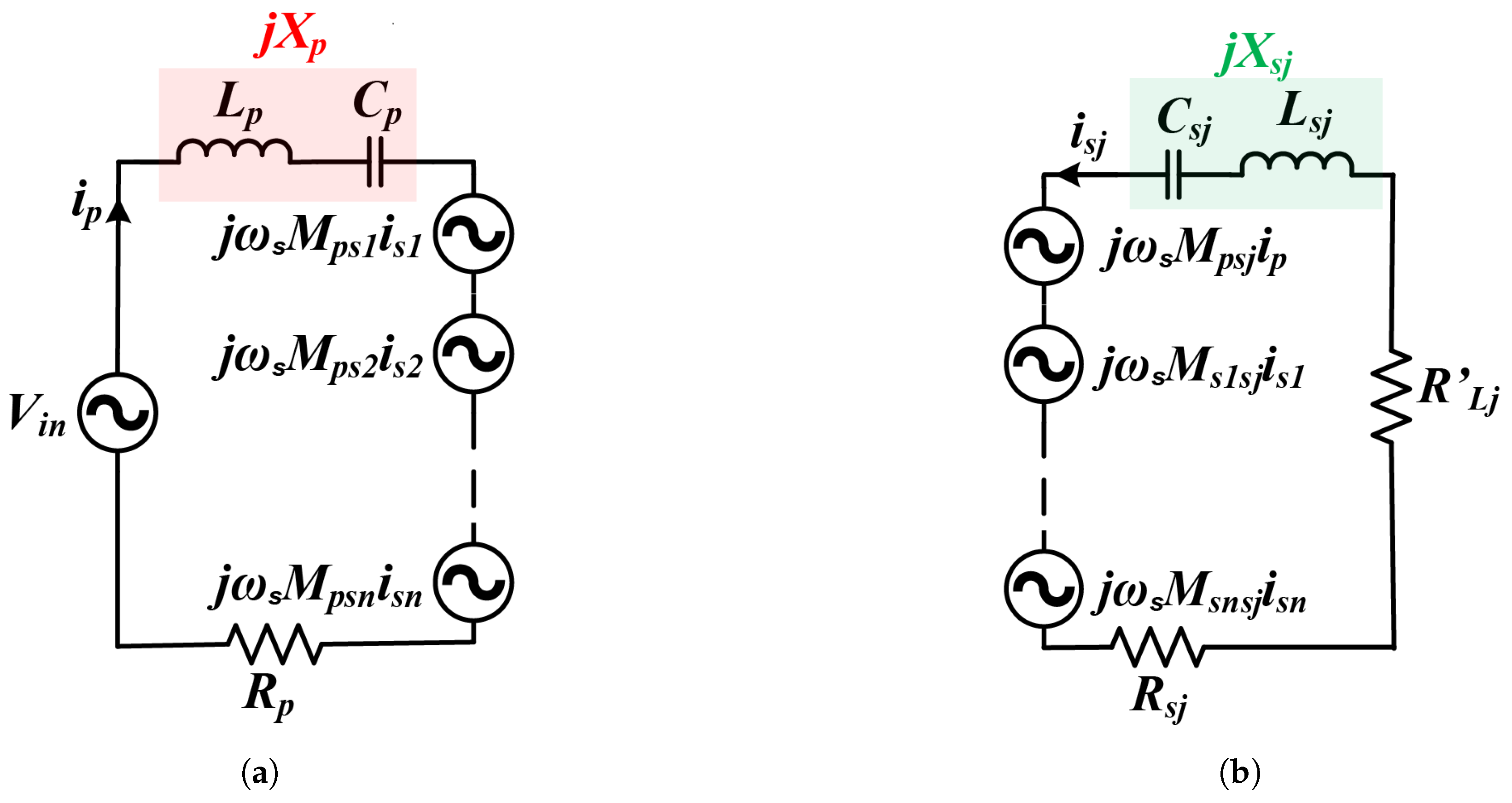
Figure 4.
Variation in efficiency () with , with change in (a) load resistances and with and , respectively, and (b) coupling factors and with and , respectively.
Figure 4.
Variation in efficiency () with , with change in (a) load resistances and with and , respectively, and (b) coupling factors and with and , respectively.
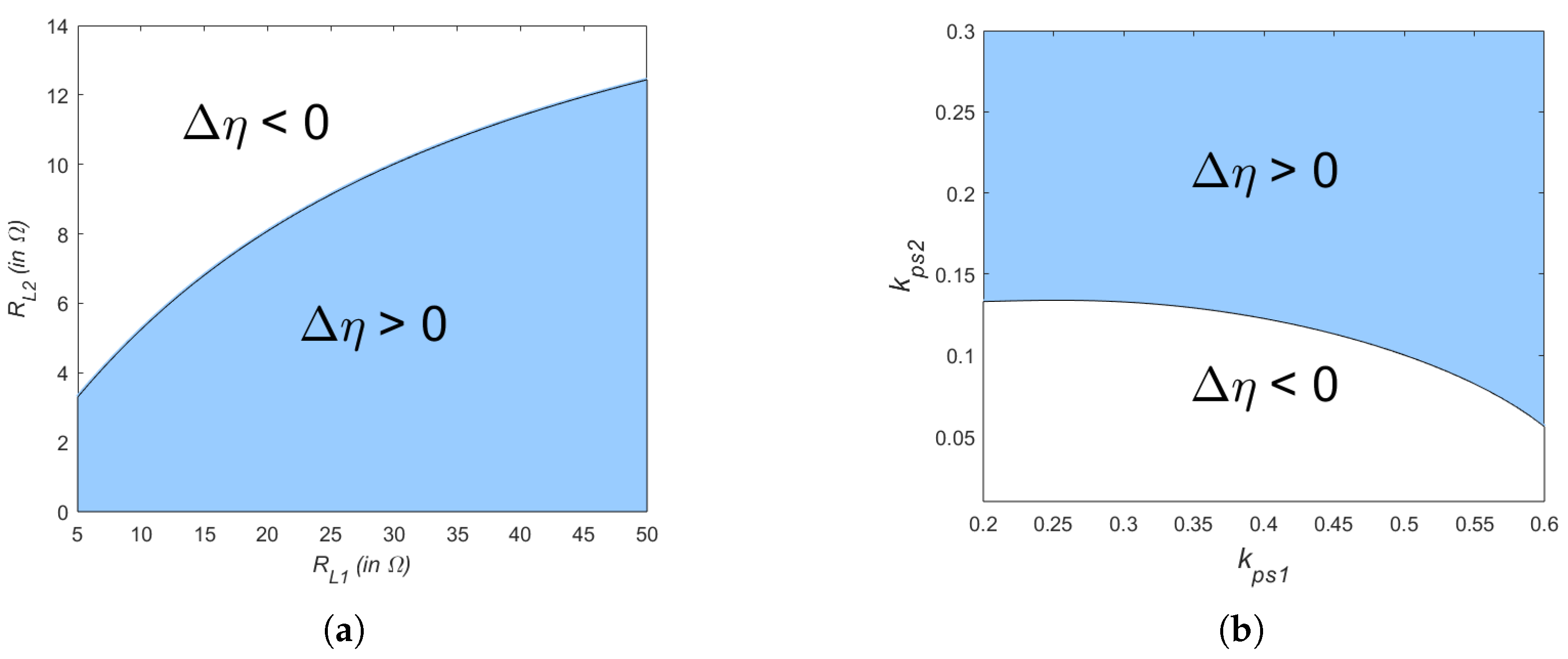
Figure 5.
Variation in efficiency () with , with change in (a) load resistances and with and , respectively, and (b) coupling factors and with and , respectively.
Figure 5.
Variation in efficiency () with , with change in (a) load resistances and with and , respectively, and (b) coupling factors and with and , respectively.
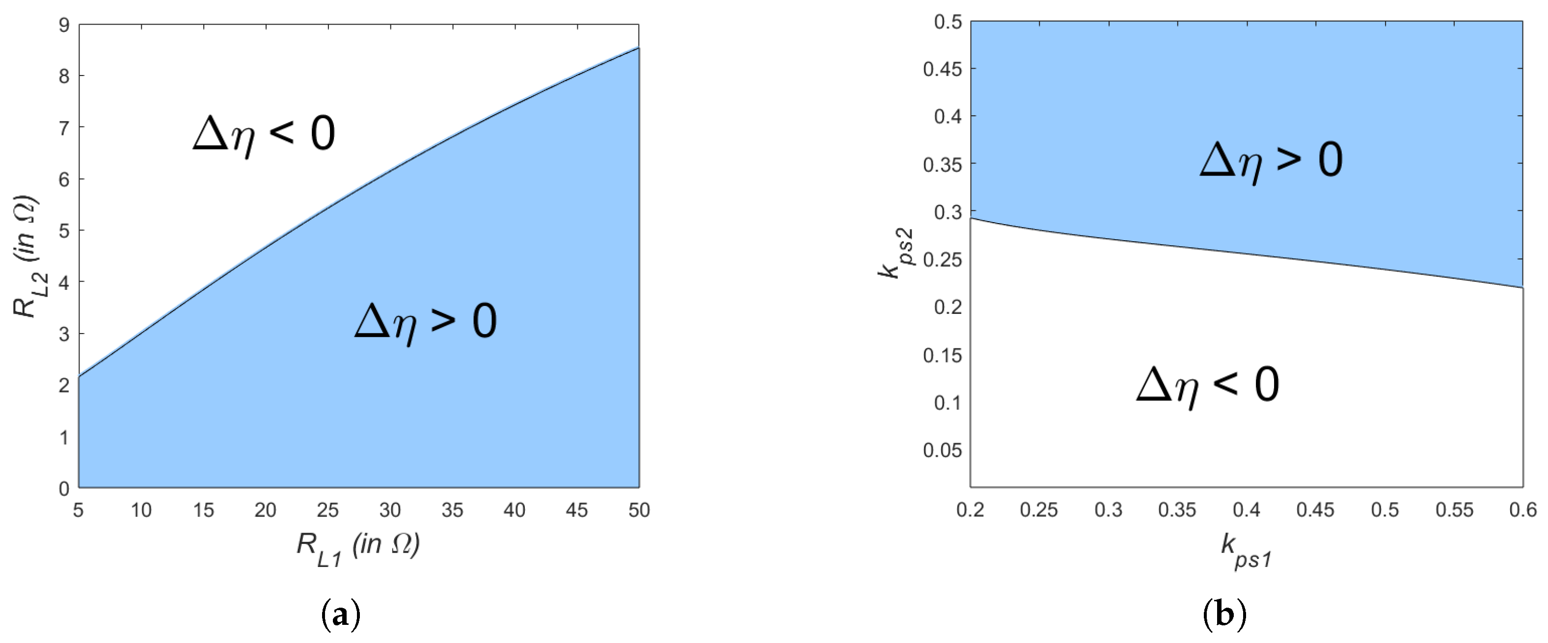
Figure 6.
Switched-capacitor network: (a) circuit and (b) key waveforms.
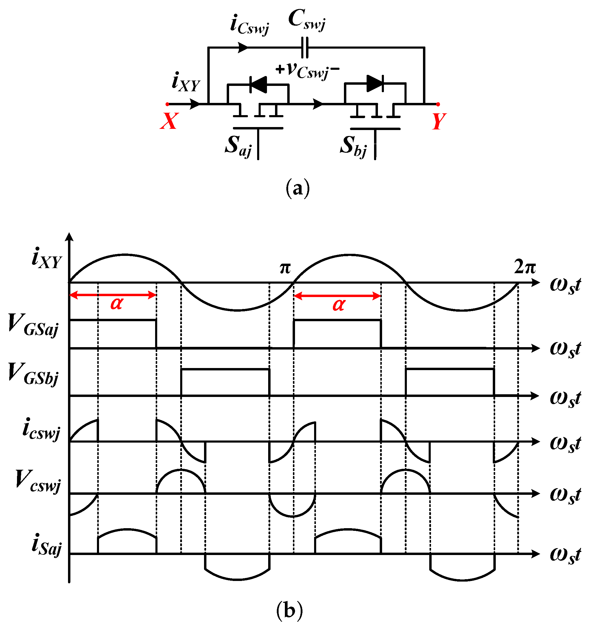
Figure 7.
Variation in as a function of when (1) , (2) and (3) .

Figure 8.
Analytical plots as a function of relative resonant frequencies for (a) link efficiency, (b) RMS current through the transmitter coil, (c) RMS current through receiver 1 coil and (d) RMS current through receiver 2 coil in a two-receiver WPT system with , , , and .
Figure 8.
Analytical plots as a function of relative resonant frequencies for (a) link efficiency, (b) RMS current through the transmitter coil, (c) RMS current through receiver 1 coil and (d) RMS current through receiver 2 coil in a two-receiver WPT system with , , , and .

Figure 9.
Flowchart of the dynamic tracking algorithm for optimizing efficiency for n receivers.
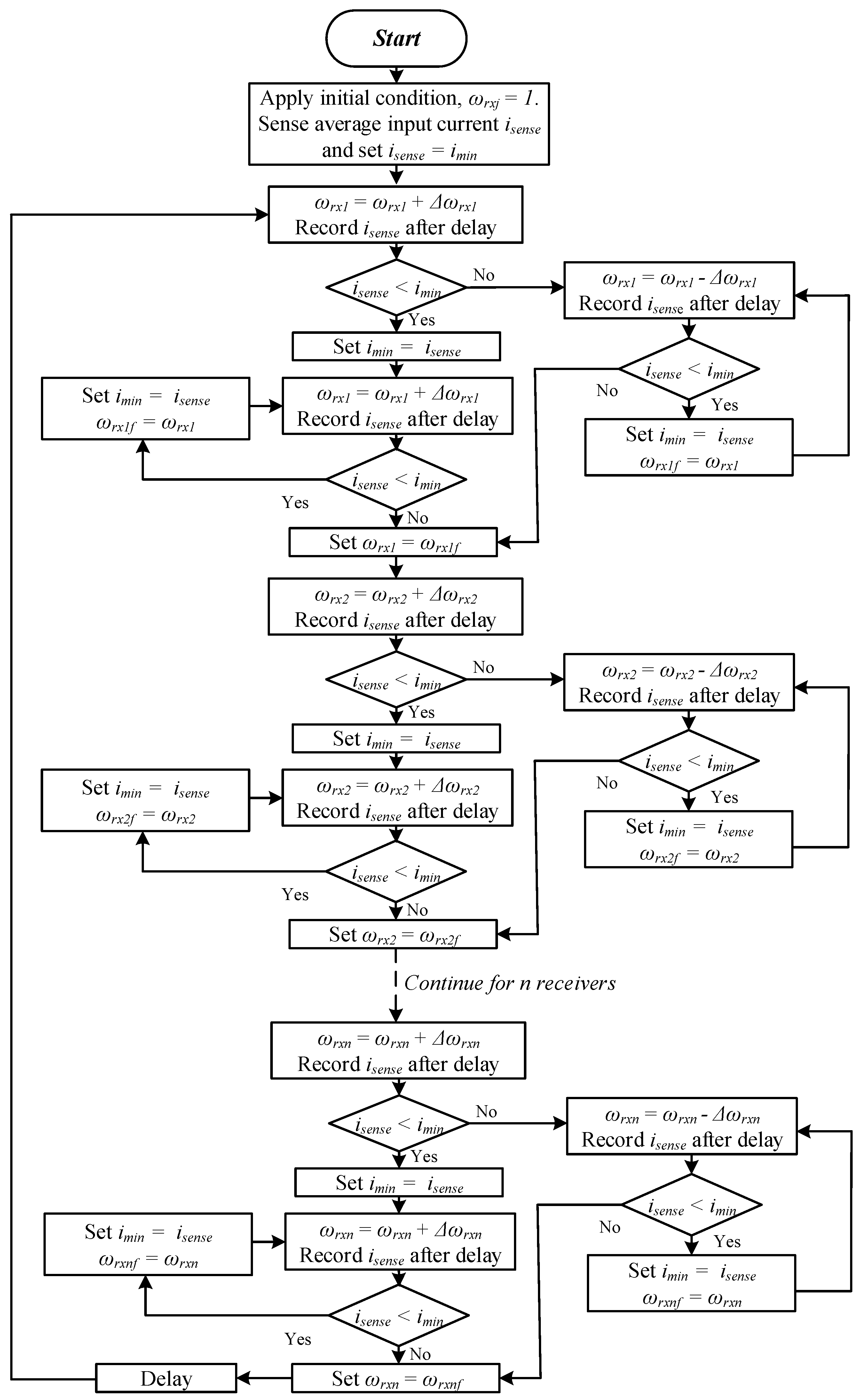
Figure 10.
(a) Circuit diagram and (b) printed circuit board of the proposed WPT receiver system.
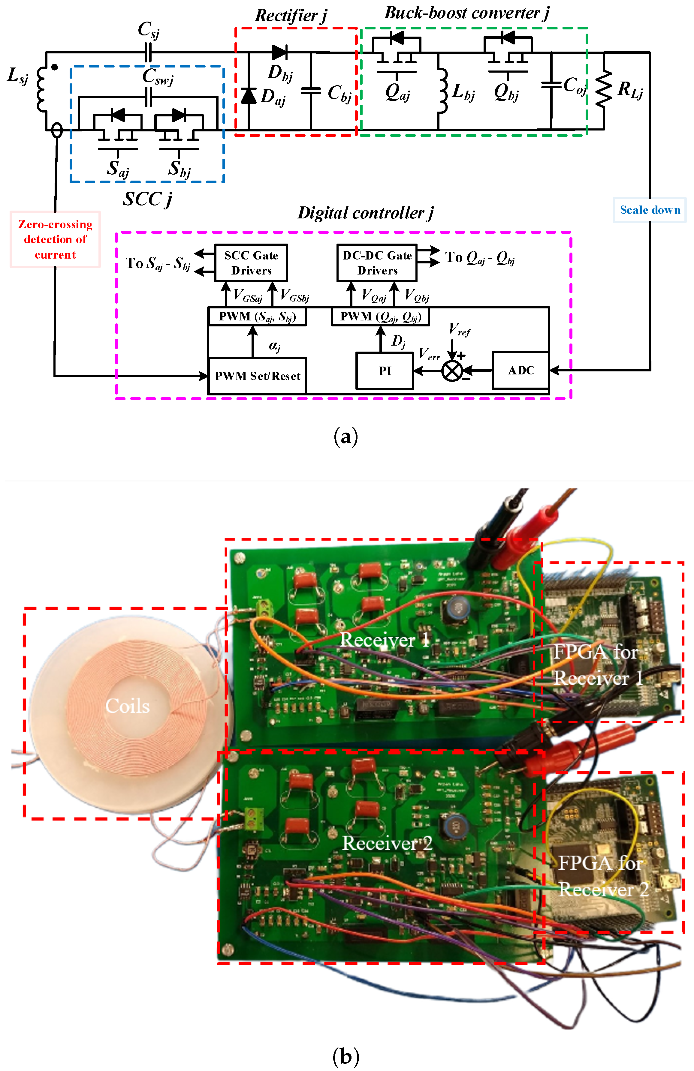
Figure 11.
Experimental waveforms of (a) input voltage and current , (b) currents and and (c) currents and at the beginning of the algorithm when both the receivers were operating at full load (: 10 V/div, : 1 A/div, , : 5 V/div, : 1 A/div, : 1 A/div, , : 5 V/div, : 1 A/div, : 1 A/div).
Figure 11.
Experimental waveforms of (a) input voltage and current , (b) currents and and (c) currents and at the beginning of the algorithm when both the receivers were operating at full load (: 10 V/div, : 1 A/div, , : 5 V/div, : 1 A/div, : 1 A/div, , : 5 V/div, : 1 A/div, : 1 A/div).
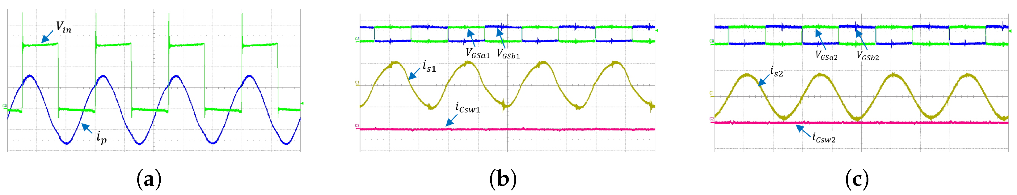
Figure 12.
Experimental waveforms of (a) input voltage and current , (b) currents and and (c) currents and at the end of the algorithm when both the receivers were operating at full load (: 10 V/div, : 1 A/div, , : 5 V/div, : 1 A/div, : 1 A/div, , : 5 V/div, : 1 A/div, : 1 A/div).
Figure 12.
Experimental waveforms of (a) input voltage and current , (b) currents and and (c) currents and at the end of the algorithm when both the receivers were operating at full load (: 10 V/div, : 1 A/div, , : 5 V/div, : 1 A/div, : 1 A/div, , : 5 V/div, : 1 A/div, : 1 A/div).
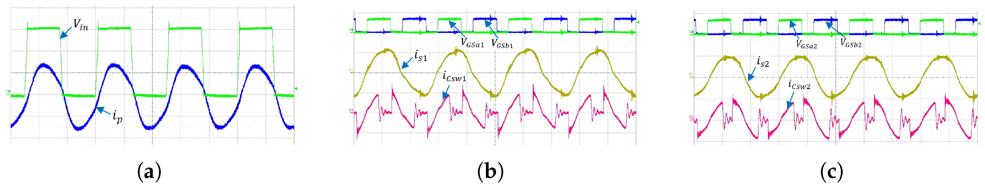
Figure 13.
Experimental waveforms of (a) input voltage and current , (b) currents and and (c) currents and at the beginning of the algorithm when Receiver 1 was operating at full load and Receiver 2 was operating at light load () (: 10 V/div, : 1 A/div, , : 5 V/div, : 1 A/div, : 1 A/div, , : 5 V/div, : 500 mA/div, : 500 mA/div).

Figure 14.
Experimental waveforms of (a) input voltage and current , (b) currents and and (c) currents and at the end of the algorithm when Receiver 1 was operating at full load and Receiver 2 was operating at light load () (: 10 V/div, : 1 A/div, , : 5 V/div, : 1 A/div, : 1 A/div, , : 5 V/div, : 500 mA/div, : 500 mA/div).
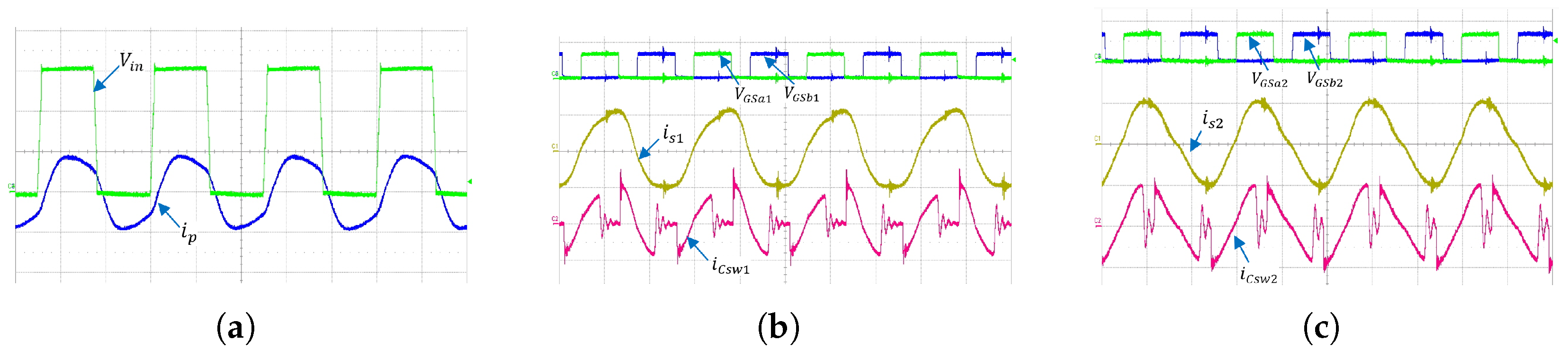
Figure 15.
(a) Variation of the control angles and and (b) variation of system efficiency during the course of the algorithm when both the receivers were operating at full load.
Figure 15.
(a) Variation of the control angles and and (b) variation of system efficiency during the course of the algorithm when both the receivers were operating at full load.
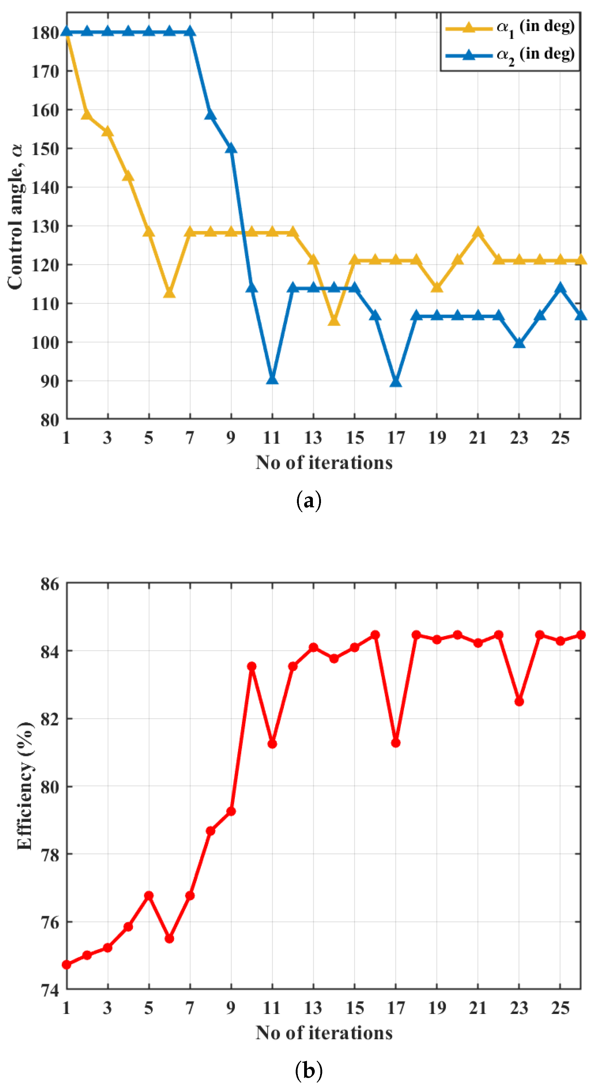
Figure 16.
(a) Variation of the control angles and and (b) variation of system efficiency during the course of the algorithm when one receiver was operating at full load and the other receiver was operating at light load ().
Figure 16.
(a) Variation of the control angles and and (b) variation of system efficiency during the course of the algorithm when one receiver was operating at full load and the other receiver was operating at light load ().


Table 1.
Wireless power transfer system specifications for Analysis.
| Symbol | Parameter | Value |
|---|---|---|
| Input voltage | 30 V | |
| Output voltage | 5 V | |
| Rated output power | 5 W | |
| Switching frequency | 200 kHz | |
| Transmitter and receiver coil inductance | 24 H | |
| Transmitter- and receiver-side resistance | 0.3 | |
| Transmitter- and receiver-side capacitance | 26.38 nF |
Table 2.
WPT system specifications of the experimental prototype.
| Symbol | Parameter | Value |
|---|---|---|
| Input voltage | 30 V | |
| Output voltage | 5 V | |
| Rated output power | 5 W | |
| Switching frequency | 200 kHz | |
| Transmitter coil inductance | 24.2 H | |
| Receiver 1 coil inductance | 23.7 H | |
| Receiver 2 coil inductance | 23.6 H | |
| Transmitter-side resistance | 0.58 | |
| Receiver-side resistance | 0.44 | |
| Receiver-side resistance | 0.45 | |
| Transmitter-side capacitance | 26.38 nF | |
| Receiver 1 capacitance | 26.38 nF | |
| Receiver 2 capacitance | 26.38 nF | |
| Coupling between Transmitter and Receiver 1 | 0.39 | |
| Coupling between Transmitter and Receiver 2 | 0.25 | |
| Coupling between Receiver 1 and Receiver 2 | 0.65 |
Table 3.
A comparative study between the proposed and existing research works on WPT systems with multiple receivers.
Table 3.
A comparative study between the proposed and existing research works on WPT systems with multiple receivers.
| Research Works | Simultaneous Power Transfer to Multiple Receivers | Requirement of Estimation Techniques | Possibility to Add More Receivers After Design | Complexity of Design | Operating Range of Load and Coupling |
|---|---|---|---|---|---|
| Coil decoupling [18,19,20] | Yes | No | No (Coils need to have a specific design for a specific number of receivers.) | Medium (Coil design can be complicated for more than two receivers.) | Narrow |
| Multi-resonant [21,22,23,24] | Yes | No | Yes (However, the number of receivers is limited by the available frequencies.) | Medium (Needs additional circuitry for filtering noise and avoiding interference with other receivers.) | Narrow |
| Time division multiplexing [25,26] | No | No | Yes (However, addition of more receivers further limits duration of power delivery.) | Low (Design is straightforward, as one receiver is powered at a time.) | Wide |
| Passive compensation [27] | Yes | No | No (Coils and compensation networks need to be redesigned for more receivers.) | Low (Design is fairly straightforward once the number and specifications of target receivers are finalized.) | Narrow |
| Active reactance compensation [15,28] | Yes | Yes | Yes (However, more parameters would need estimation to apply the required reactance to the receivers.) | High (Estimation algorithms for system parameters could be computationally intensive.) | Wide |
| Current quadrature phenomena [30,31] | Yes | No | Yes (However, phase information of the transmitter current is required to be communicated to the receivers.) | Medium (Needs automatic tuning assist circuit or switched capacitor circuits for orthogonalization of the transmitter and receiver currents.) | Narrow |
| Proposed technique | Yes | No | Yes (Power can be delivered to more receivers within the rating of the transmitter components.) | Medium (Needs additional switched-capacitor circuit for modulating receiver reactance.) | Wide |
Publisher’s Note: MDPI stays neutral with regard to jurisdictional claims in published maps and institutional affiliations. |
© 2022 by the authors. Licensee MDPI, Basel, Switzerland. This article is an open access article distributed under the terms and conditions of the Creative Commons Attribution (CC BY) license (https://creativecommons.org/licenses/by/4.0/).
Share and Cite
MDPI and ACS Style
Laha, A.; Kalathy, A.; Pahlevani, M.; Jain, P. A Real-Time Maximum Efficiency Tracker for Wireless Power Transfer Systems with Cross-Coupling. Electronics 2022, 11, 3928. https://doi.org/10.3390/electronics11233928
AMA Style
Laha A, Kalathy A, Pahlevani M, Jain P. A Real-Time Maximum Efficiency Tracker for Wireless Power Transfer Systems with Cross-Coupling. Electronics. 2022; 11(23):3928. https://doi.org/10.3390/electronics11233928
Chicago/Turabian StyleLaha, Arpan, Abirami Kalathy, Majid Pahlevani, and Praveen Jain. 2022. "A Real-Time Maximum Efficiency Tracker for Wireless Power Transfer Systems with Cross-Coupling" Electronics 11, no. 23: 3928. https://doi.org/10.3390/electronics11233928
Note that from the first issue of 2016, this journal uses article numbers instead of page numbers. See further details here.