Abstract
Multilevel converters continue their upward trend in renewable generation, electric vehicles, and power quality conditioning applications. Despite having satisfactory voltage capabilities, mainstream multilevel converters suffer from poor current sharing performances, thereby leading to the development of lattice converters, i.e., a strong and versatile type of future multilevel power converters. This article addresses two problems faced by lattice converters. First, we propose and detail how to optimize the efficiency of a given lattice converter by controlling the on/off states of H-bridge submodules. Second, we introduce the method that determines the voltage at each node of the converter in order to satisfy output voltage and current requirements. Design and analysis of lattice converters need a different mathematical toolbox than routinely exercised in power electronics. By use of graph theory, this article provides control methods of 3 × 3 and 4 × 4 lattice converters, satisfying various control objectives such as input/output terminals and output voltages. We further validate the methods with simulation results. The methodologies, algorithms, and special cases described in the article will aid further design and refinement of more efficient and easy-to-control lattice converters.
1. Introduction
Cascaded-bridge converters (CBCs) and modular multilevel converters (MMCs) are being applied in an increasing number of fields due to their advantages such as modularity and scalability [1,2,3]. High voltage power transmission [3,4,5,6], renewable energy generation [7,8,9,10,11], electric vehicles [12,13,14,15,16,17,18], power quality conditioning [19,20,21], transformers [22,23,24], and power supplies [25,26,27] are some of the fields where multilevel converters start to gain growing popularity. Modular multilevel converters and their variations are particularly beneficial because of their high output quality, harmonic spectrum, adequate dynamic response, low in su la tion and bearing stress due to more moderate voltage transients dV/dt, failure tolerance, modularity in man u fac turing and replacement, reach of practically any high voltage and power level with relatively low-voltage com po nents, scalability, and lower switching losses [1,28,29,30,31,32,33].
In spite of the forenamed advantages, classic modular multi level converters are limited in many aspects. They have weak current sharing capabilities [1,34], reduced efficiency at lower voltages, and stricter voltage balancing requirements [34,35]. These shortcomings motivate the introduction of parallel connectivity to MMCs [34,35,36,37,38,39,40]. Such developments give rise to MMCs with serial and parallel connectivity (MMSPCs), which enjoy both expanded current capabilities and the privilege of simple and even sensorless voltage balancing algorithms [34,40,41,42,43].
Although implementing parallel connectivity between neighboring submodules provide a number of benefits, MMSPCs are still limited since they are serial on the macro-level, meaning that the overall modules cannot be paralleled. Therefore, lattice converters are proposed to connect individual converter modules both in series and in parallel to form a lattice grid [36,43]. Lattice converters have large (up to infinite) voltage/current conversion capabilities, multiple input/output terminals that allow free connection to various circuits, as well as simple modular expansion abilities. In summary, compared to traditional MMCs, lattice converters have higher upper limits for volage and current capabilities, improved modularity and scalability, and more versatility.
Figure 1a shows an example of the wiring diagram of a simple 3 × 3 latice converter, with each submodule being an H-bridge converter powered with a DC voltage source. Figure 1b shows the schematics of 3 × 3 and 4 × 4 grid lattice converter examples, where the numbered points are denoted as nodes and the lines connecting nodes are edges, which, in general, can be H-bridges, symmetrical half-bridges, asymmetrical half-bridges, or the other submodules in [1]. In this article, all edges are considered H-bridges to offer the most control freedom, since they can execute one of the four functions: raise the voltage, lower the voltage, keep the voltage unchanged, or bypass the edge. Through the combination of individual H-bridge controls (which will be explained in more detail in Section 2), the lattice converter as a whole can output different voltages.
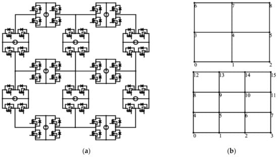
Figure 1.
Schematics of Lattice Converters: (a) Example of 3 × 3 Lattice Converter wiring diagram. Each edge is an H-bridge converter, shown with more details in Section 2.1; (b) Schematic of a 3 × 3 Lattice Converter (Above); Schematic of a 4 × 4 Lattice Converter (Below).
While lattice converters outstrip other modular multilevel converters with increased freedom and broader applications, their advantages come at the cost of added control complexity. As shown in Figure 1a, a simple 3 × 3 lattice converter consists of 12 edges, each representing an H-bridge with four possible states, offering a large number of controllable degrees of freedom. Among the many control options, some are especially desirable because of their high efficiency and viability.
In order to find the preferable control options, this article focuses on two problems: efficiency optimization and node voltage solution. Section 2 explains the modeling process of lattice converters that sets the ground for further analyses. Section 3 introduces the algorithm to solve the two problems and find the optimized control options in details. Section 4 presents the results and analyses regarding 3 × 3 and 4 × 4 lattice converters. Section 5 summarizes the article.
2. Fundamentals and Modeling of Lattice Converters
2.1. Lattice Converters and H-Bridges
As discussed in Section 1, lattice converters are controlled via the manipulation of individual edges, or H-bridges. This section briefly discusses H-bridge control. Figure 2 shows an example of the H-bridge utilized in lattice converters. A particular H-bridge consists of four semiconductor switches and a voltage source, either a battery or a capacitor. Assuming the current flowing in through the left terminal and flowing out from the right terminal, the H-bridge can perform one of the four voltage conversion functions by controlling the on/off states of the switches. In the first state, +1, the H-bridge outputs a positive voltage of Vdc by turning on switches S2, S3. Alternatively, the H-bridge can be in the state of –1, lowering the voltage by Vdc by turning on switches S1, S4. The third state 0 is a short circuit with all upper/lower switches on. Finally, the off state is an open circuit with all switches off. Open circuit H-bridges are fundamentally different from the other three, since it alters the topology of the lattice converter, and thus is named differently from other states. The fact that each edge can have four different states makes lattice converters extremely versatile, enabling them to be controlled and optimized to serve a wide range of purposes.
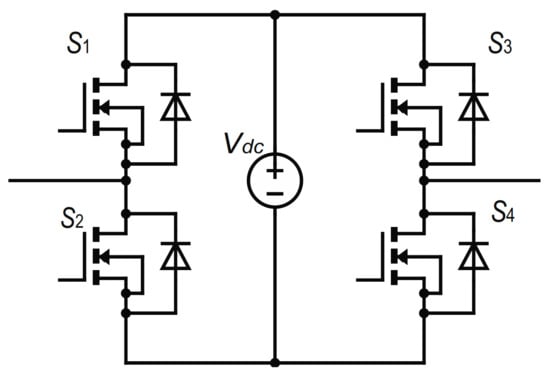
Figure 2.
An H-bridge Used as an Edge in Lattice Converters.
2.2. Modeling of Lattice Converters
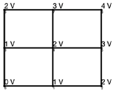
Graph theory serves to solve the two aforementioned problems and describe complicated lattice structures formally. We treat lattice converters as graphs consisting of nodes and edges. Connected edges represent H-bridges in either +1, –1, or 0 states. If two nodes are next to each other in the vertical or horizontal direction but are not connected by an edge, then there is an off H-bridge in-between. Each node is numbered, and the lattice graph is represented as an adjacency matrix. For a grid lattice of size a × a, the adjacency matrix is an a2 × a2 symmetric matrix. If the state of an H-bridge connecting two nodes (x, y) is not off, the matrix elements on the xth row and yth column as well as the yth row and xth column of the adjacency matrix would be 1, while otherwise being 0. Figure 3 shows an example of such an adjacency matrix.
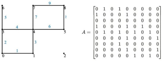
Figure 3.
Adjacency Matrix of the 3 × 3 Lattice Converter Shown.
With the help of the adjacency matrix, it is possible to find paths that electrical currents go through when traveling across the lattice converter. Given a pair of starting and destination nodes, such paths can be extracted and represented as a sequence of nodes through which currents travel. In Figure 3, for example, a path starting from node 0 and ending at node 8 can be [0, 1, 4, 5, 8]. This path is reflected in the adjacency matrix by the elements (1, 2), (2, 5), (5, 6), (6, 9), being one.
A lattice graph can therefore be viewed as a combination of paths, making it simple to optimize efficiencies and solve for node voltages.
3. Efficiency Optimization Calculations and Node Voltage Solutions
3.1. Efficiency Optimization
Lattice converter efficiency optimization is desirable due to the large number of control options even with strict requirements, including lattice size, input/output terminals, as well as desired output voltages and currents. We find that for a lattice converter of given size, the efficiency depends solely on whether each edge is at the open circuit state (the off state) or not. Therefore, a graph indicating where the edges are connected serves as the solution to the efficiency optimization problem. In this way, most efficient solutions can help minimize dissipated energy, converting more input power to useful output power.
The method of enumeration is employed to find the best graph. All possible graphs are exhausted by paralleling different numbers of paths, i.e., from paralleling one path to paralleling all paths. The efficiencies of all possible graphs with a given size are calculated and compared.
To find the efficiency of a given graph, each H-bridge is considered to have a total internal resistance r of the voltage source and non-ideal switches. The voltage at the starting node is treated as 0 V, while the voltage at the destination node is the output voltage, Vout. The load resistance is Rload. Therefore, the efficiency η of the given lattice converter is
where
where can be found by summing the power dissipated on each H-bridge. Suppose the current passing through a particular H-bridge, α, is iα,
Therefore, the problem reduces to finding iα for each edge, for which we can create an unknown vector to be solved for. To achieve this, we write and solve the Kirchhoff current and voltage laws (KCL and KVL). Both laws can be represented using matrices corresponding to the lattice converter graph, making it simple to write down a system of linear equations and solve for the current on each edge. In this article, we use the lattice converter shown in Figure 3 to illustrate the process for writing down KCL and KVL equations.
The KCL is associated with the graph’s incidence matrix. The incidence matrix shows the relationship between nodes and edges. Each column represents an edge while each row represents a node. If the matrix element on the xth row and yth column is 1, then the edge labeled y is pointing towards the node labeled x; if the element is –1, then the edge is leaving the node; and if the element is 0, then the edge is not connected to the node. The incidence matrix of the graph shown in Figure 3 follows.
Translating this matrix into circuit languages, a + 1 represents the current flowing into the node, a − 1 means the current leaving the node, and a 0 means no current. According to each row of the incidence matrix, the KCL can then be written as
where the vector has zero entries except for the ones corresponding to the starting and the destination nodes. Letting be the output current, the vector element representing the starting nodes should be −Iout since current is flowing into the node while vector is on the other side of the equation. On the other hand, the vector element representing the destination node should be + Iout.
While this system of linear equations gives nine equations for the nine unknown edge currents in Figure 3, one of the equations is trivial (node 2 is not connected to any other nodes), necessitating the incorporation of KVL equations. To find KVL equations, we need to identify the basis cycles for a given graph. For the example shown in Figure 3, there are two basis cycles: the first consists of edges [(0, 1), (1, 4), (4, 3), (3, 0)], the second [(4, 5), (5, 8), (8, 7), (7, 4)]. Since all loops in lattice converters consist of an even number of edges, we can always define loops to be clockwise, so that they point to the same direction as the first half of edges and point to the inverse direction as the second half of edges in the loop. In addition, although each H-bridge converter has the ability to raise/lower the voltage by 1 or to keep it the same, it is assumed that each node has a unique voltage (explained more in detail in Section 3.2). This leads to the fact that the total voltage change by the H-bridge converters in each loop equals zero, leaving only the current terms in the KVL equation. We can further eliminate the internal resistance on all terms since it is the same for every edge. The KVL equations for Figure 3 can be written as
Solving systems (6) and (7) yields iα for each edge which is stored in vector . Therefore, the efficiency of the lattice converter is
Computing and comparing the efficiencies of all possible lattice converter graphs, we can find the most efficient graph. The algorithm is summarized below:
- (1)
- Given a lattice size, the adjacency matrix for a graph with all edges connected (none in the off state) is found with function MatrixGen(size) to be A;
- (2)
- All possible paths from the input node to the output node are found with AllPathStore and stored in all_path;
- (3)
- Paralleling n paths, (n running from one to all paths), a function EfficiencyOpt is applied. Inside the EfficiencyOpt function;
- First, select n paths from all_path. Then combine the n selected paths to form the new adjacency matrix, B, for the particular configuration;
- Second, apply the FindEfficiency function (Equation (8)) to find the circuit efficiency of B;
- Store the matrix B and the efficiency , and compare to find the maximum efficiency and the corresponding matrix within the loop;
- (4)
- Find the maximum efficiency and the corresponding matrix for all n’s, and construct the resulting graph from the matrix.
It is worth noting that with this algorithm, it is possible to store all the configurations with high efficiencies in order. In the case of possible damages to H-Bridge modules, preventing the optimized choice, it is easy to select another control option with highest efficiency given the constraint.
3.2. Node Voltage Solutions
Node voltage solutions are a set of voltages assigned to each node of the lattice converter. They are sufficient to fully determine the state of each edge and provide unique control algorithms. There are three conditions that node voltages must follow: (1) the voltage at the starting node is 0 V, (2) the voltage at the destination node is the desired output voltage, and (3) the voltage difference between any two connected neighboring nodes can only be +1, −1, or 0 given the four functions of H-bridges. Satisfying these conditions and with the specific voltage at each node, a lattice converter can be completely defined.
To solve for node voltages, several important assumptions are made: (1), voltage drops on each edge due to internal resistances are ignored, and (2), each node is considered to have a unique voltage.
First, although there is power dissipated when the current flows through an edge, the voltage drop invoked is ignored. Such a simplification is justified by the small internal resistance. Between two given nodes connected by an H-bridge α, let iα be the current flowing through the edge α and r be the internal resistance of the edge. The voltage drop due to power dissipation on a single edge can be represented as
In practical cases, r is rather small and iα typically moderate so that the overall voltage drop is negligible for control.
The second assumption makes sure that each node corresponds to a unique voltage value. Since each connected H-bridge can lower the voltage by Vdc, raise it by Vdc, or keep it the same, situations such as the one described in Figure 4 seem possible, where the displayed converter states lead to a disagreement on node 3. These situations are undesirable and should be avoided. Paralleling different voltage sources would generate a large amount of current, causing potential danger. In addition, a clear output voltage is required at the destination, while uncertainties regarding any nodes in-between the starting and the destination node would disturb this clarity and lead to a twisted output voltage. Given these disadvantages, invalid states such as the one shown in Figure 4 are avoided when designing lattice converters, leading to the second assumption that each node has a unique voltage while H-bridges are controlled to satisfy these node voltages.
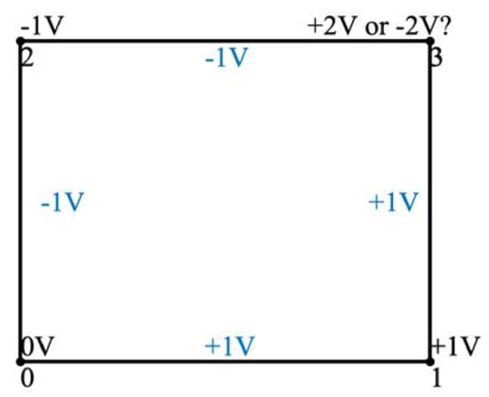
Figure 4.
Example of an invalid converter status.
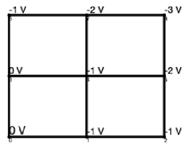
These two assumptions help simplify and clarify the problem. To explicitly solve for node voltages, we first determine the possible voltage assignments on each path. For example, if the output voltage requirement is 3, then the path [0, 1, 4, 5, 8] can have node voltages [0, 0, 1, 2, 3], [0, 1, 1, 2, 3], [0, 1, 2, 2, 3], and [0, 1, 2, 3, 3].
Then, path voltages are combined and the ones compatible (per the second assumption) are kept. Therefore, each node receives a unique voltage assignment that is consistent with the output voltage requirements. The solution would then determine how to control individual H-bridges. The algorithm is summarized below:
- (1)
- Given a lattice configuration A, all possible paths from the starting to the destination nodes are found and stored in all_path with AllPathStore;
- (2)
- Find the range of possible voltages for each node. This step is important to simplify the algorithm and reduce the computation time. For the input node, both the lower and upper limits are 0. For the output node, both are the desired output voltage. For any undefined node in-between, we first start from the input node to find the possible range by looking at a connected node with previously defined voltage ranges. We then perform the same algorithm but starting from the output node. We compare the ranges obtained from both directions and record the greater lower limit and smaller upper limit. For example, with a desired output voltage of 2 V and the circuit configuration shown in Figure 3, we first define the range for node 0 to be [0, 0] and the range for node 8 to be [2, 2]. Then, starting from node 0, for node 1 and 3, the voltage range can be [−1, 1]; for nodes 4 and 6, [−2, 2]; for nodes 5 and 7, [−3, 3]. Starting from node 8, we have for nodes 7 and 5, [1, 3]; for nodes 4 and 6, [0,4]; for nodes 1 and 3, [−1, 5]. Comparing both, we obtain voltage ranges for nodes 1 and 3, [−1, 1]; for node 4, [0, 2]; for node 6, [−2, 2]; and for nodes 5 and 7, [1, 3];
- (3)
- For each path, we find the possible path voltage combinations by combining possible voltages of individual nodes passed by the path. Continuing the previous example, with a path passing through nodes [0, 1, 4, 7, 8], we have the possible voltage ranges for each node: {[0, 0], [−1, 1], [0, 2], [1, 3], [2, 2]}, which means the possible voltage values for each node are {[0], [−1, 0, 1], [0, 1, 2], [1, 2, 3], [2]}. Looping through all combinations and keeping only the ones meeting requirement of voltage differences with connecting nodes, we obtain 10 possible path voltages: [0, −1, 0, 1, 2], [0, 0, 0, 1, 2], [0, 0, 1, 1, 2], [0, 0, 1, 2, 2], [0, 1, 0, 1, 2], [0, 1, 1, 1, 2], [0, 1, 1, 2, 2], [0, 1, 2, 1, 2], [0, 1, 2, 2, 2], [0, 1, 2, 3, 2];
- (4)
- Finally, we combine the path voltages if they are compatible with each other. We first turn the path voltages into node voltages by inserting them into arrays where the index correspond to the node number, i.e., turn [0, −1, 0, 1, 2] into [0, −1, x, x, 0, x, x, 1, 2], where the “x” indicates that this node voltage has not be specified yet. For two node voltages to be compatible, voltage on each node must be either (1) the same for both, (2) unspecified for one, or (3) unspecified for both. If either of the conditions is met, the two path voltages will be combined into one single output. For the example we have been using, we obtain 34 distinct node voltage solutions.
4. Results
4.1. Setup and Finding Paths
The complexity of a lattice converter largely depends on its size. If a lattice is of size a × a, then it has a2 nodes and edges. Figure 5 shows the growth of number of nodes/edges as the lattice expands.
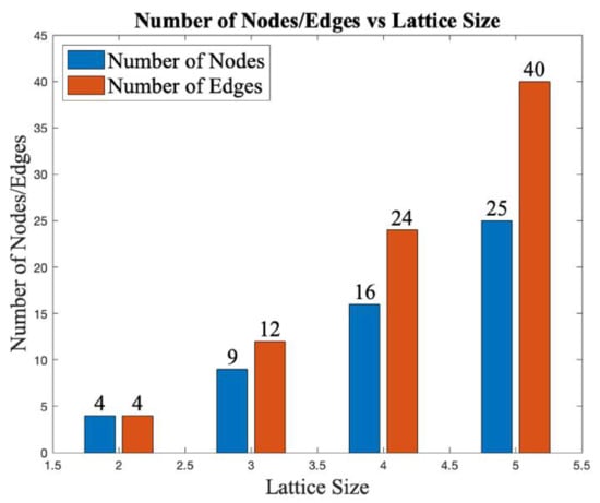
Figure 5.
Number of nodes/edges as a function of lattice sizes.
The increasing complexity of lattice converters is reflected in the total number of paths. The total number of paths depends on the starting node and the destination node, as well as the lattice size. Using the path-finding method described in Section 2.1 and counting the resulting paths between two nodes, the total number of paths can be determined. Given that all starting nodes are in the bottom left corners, and all destination nodes are in the top right corners, the relationship between the number of paths and the lattice size are listed as follows: a size-2 lattice has 2 paths; a size-3 lattice has 12 paths; a size-4 lattice has 184 paths; a size-5 lattice has 8512 paths, etc. We show that expanding the lattice size by one would result in an exponential growth in number of paths. While such expansion adds extra degrees of freedom to lattice converters, it also makes them much more difficult to control.
Therefore, this paper focuses on smaller lattice size such as 3 × 3 and 4 × 4, which are simpler to examine while preserving the versatility and intricacy of lattice converters. For a fully connected 3 × 3 lattice, we find 12 paths from node 0 to node 8. Two examples are shown in Figure 6.
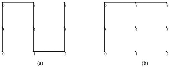
Figure 6.
Example paths between nodes 0 and 8: (a) Path [0,3,6,7,4,1,2,5,8]; (b) Path [0,3,6,7,8].
Table 1 shows the classification of all paths for a 3 × 3 lattice. Path size is described by how many edges the particular current path passes through. Such a categorization is especially useful in the application of efficiency optimization, since longer paths represent larger internal resistance, given similar total voltage and current conditions.

Table 1.
Classification of 3 × 3 lattice paths from node 0 to node 8 according to Path Size.
4.2. Efficiency Optimization
4.2.1. 3 × 3 Lattice Converter
For a lattice converter of size 3 × 3, we find and compare the efficiencies of all possible graphs using the algorithm introduced in Section 3.1. We first choose the input port to be node 0 and the output port to be node 8. We then find all graphs by combining n number of paths, looping n from one to twelve paths for the 3 × 3 lattice. For example, when combining three paths, three out of the twelve paths shown in Table 1 are selected at random and paralleled to form a graph. We find that the most efficient 3 × 3 lattice graph is the one that is fully connected, as shown in Figure 7. In particular, with a load resistance of 10 Ω and internal resistance of 0.01 Ω, the maximum efficiency achieved with Figure 7 is 99.85%.
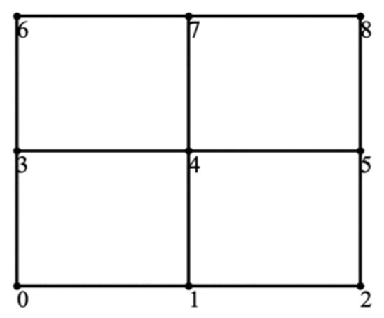
Figure 7.
Most efficient graph for 3 × 3 lattice converter from node 0 to node 8.
This result matches the intuition that paralleling more paths leads to a decreased current on each path, therefore resulting in increased efficiency. In addition, the symmetry allows the output current to be shared evenly among edges, avoiding high dissipated power on particular H-bridge converters.
Figure 8 shows the relationship between maximum/minimum efficiencies and the number of paths paralleled. Although there are fluctuations, adding more paths significantly reduces the difference between maximum and minimum efficiencies. When 8 out of the 12 paths are paralleled, all edges are connected, leading to the coincidence between maximum and minimum efficiencies. The lattice converter has a minimum efficiency of 99.2% when there is one path of size 8, and it has a maximum efficiency of 99.85% when two or more paths are paralleled to form a fully connected lattice, achieving a 0.66% difference between the two extreme cases.
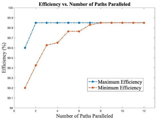
Figure 8.
Maximum and minimum efficiencies for given number of paths paralleled for 3 × 3 lattice converter.
Similar results can be obtained for other starting and destination nodes. We select a different pair of input/output terminals, find all possible graphs, and compute the efficiencies corresponding to each graph. We then compare the results and keep the most efficient graph. Figure 9 shows the most efficient graph for a lattice converter starting from Node 0 and outputting at Node 6. With the same load and internal resistance conditions, the best efficiency is 99.87%.
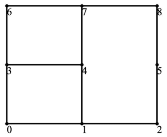
Figure 9.
Most efficient graph for 3 × 3 lattice converter from node 0 to node 6.
4.2.2. 4 × 4 Lattice Converter
For a 4 × 4 lattice from node 0 to Node 15, the most efficient graph is again the fully connected one, shown in Figure 10. A similar conclusion can be drawn that the most efficient graphs are the ones that parallel as many paths as possible. The efficiency of this graph with load resistance of 10 Ω and internal resistance of 0.01 Ω is 99.81%.
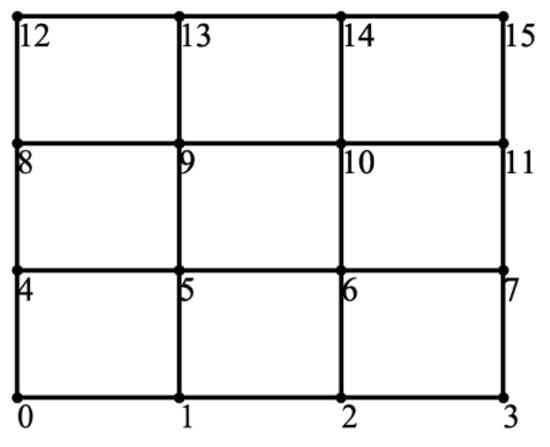
Figure 10.
Most Efficient Graphs for 4 × 4 Lattice Converter from Node 0 to Node 15.
4.2.3. Internal and Load Resistances
While all previous efficiency data are based on output voltage of 3 (3 × 3) or 5 (4 × 4), load resistance of 10 Ω, internal resistance of 0.01 Ω for each edge, and 1 voltage source for each edge, these conditions can vary, and we should examine the effect of such variations to the efficiencies of the lattice graphs. Analyses show that neither output voltage nor converter voltage affects converter efficiency, while both load and internal resistances affect it. The first subplot of Figure 11 shows the efficiency of the lattice converter shown in Figure 7 raising with a slowing rate as the load resistance increases. The second subplot of Figure 11 shows a reverse trend of efficiency decreasing (almost linearly) as internal resistance increases. Both trends are straightforward in showing that a larger difference between load resistance and internal resistance (when the difference remains positive) would result in higher efficiency.
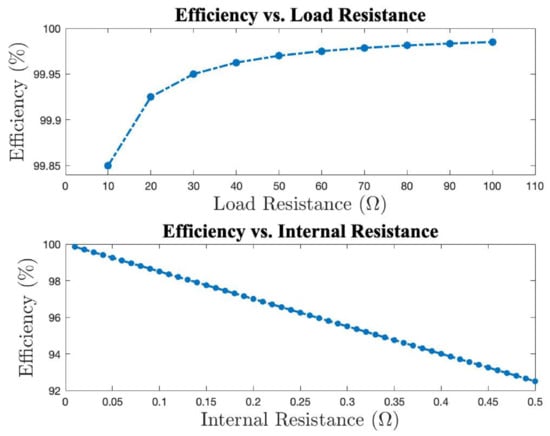
Figure 11.
Efficiency of the lattice converter shown in Figure 8 increasing with a slowing rate as load resistance increases and decreasing linearly as internal resistance increases.
However, t is worth noting that when the discrepancy between the load and internal resistances becomes too small, the lattice converter may not be able to output the desired voltage due to increased power dissipation and voltage drop on individual edges.
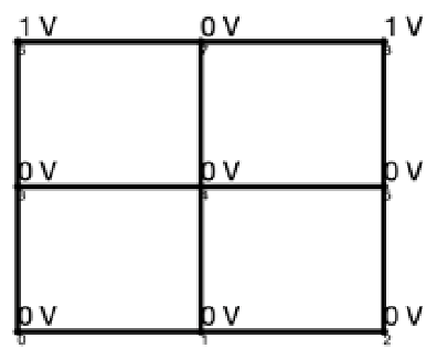
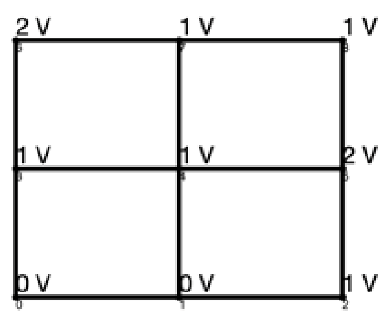
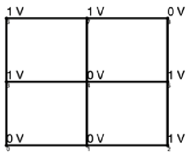
4.3. Node Voltage Solution
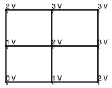
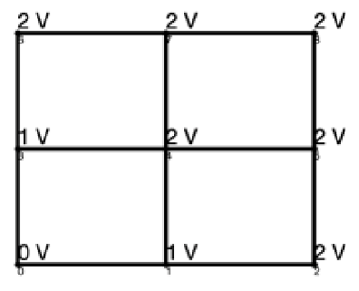
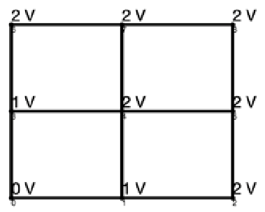
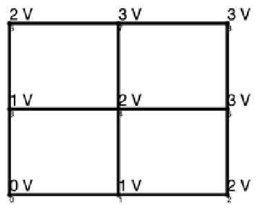
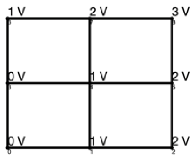
Given the most efficient graphs and a desired output voltage, there are a number of possibilities for node voltage solutions. For example, there are 18 different solutions to the most efficient 3 × 3 lattice graph shown in Figure 7 with output voltage of 3, two of which are shown in Figure 12 with different colors representing different control strategies. Similarly, there are 144 solutions to the most efficient 4 × 4 lattice shown in Figure 10 with output voltage 5, one of which is shown in Figure 13. Each of these graphs finalizes the control actions taken at each edge, providing a complete control strategy for the lattice converter.
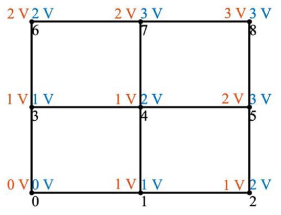
Figure 12.
Node voltage solutions for 3 × 3 lattice converter shown in Figure 7. Orange: first solution; blue: second solution.
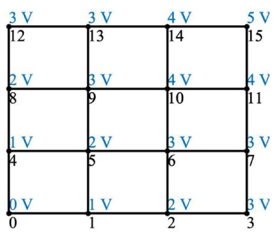
Figure 13.
Node voltage solutions for 4 × 4 lattice converter shown in Figure 10.
The total number of solutions depends on both lattice converter topology and output voltage. For the most efficient topologies shown in Figure 7 and Figure 10, the maximum output voltage can be ±4, ±6, respectively. As the absolute value of the output voltage approaches the maximum, the number of possible node voltage solutions drops rapidly. Figure 14 shows such a trend for the example of a 3 × 3 lattice converter.
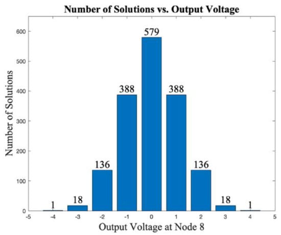
Figure 14.
Number of solutions in relation to output voltage for 3 × 3 lattice converter shown in Figure 7.
4.4. Simulation Results
We built a model in MATLAB/Simulink and simulated both 3 × 3 and 4 × 4 lattice converters with varying control strategies and measured (1) currents on each H-bridge to validate the efficiency calculations, and (2) the output voltage to validate the node voltage solutions.
In practical power converters, the DC voltage source output will typically be 200 V, with the internal resistance typically being 0.9 Ω. In our simulation, we keep all DC voltages sources at 1 V for simplicity. To match the scale, we take all internal resistances to be 0.01 Ω.
For the control strategy represented by blue shown in Figure 12, the predicted current on each edge versus the simulated current on each edge are shown in Table 2. The average relative difference between the theoretical and simulated current on each corresponding edge is only 0.14%, indicating that there is no statistical difference between the predicted and simulated data. The output voltage across the load resistance is 2.996 V, within 0.13% difference of the required output. The simulated output voltage and current do not change with time since the circuit is at its DC steady state.
Table 2.
Theoretical and simulated currents on each edge for the control strategy represented by blue shown in Figure 12.
A similar simulation is performed for the control strategy shown in Figure 13. The average difference between the calculated and simulated currents on each edge is 0.21%. The output voltage is 4.991 V, within the 0.18% difference of the required output.
Figure 15 shows the efficiency comparison between an array of different lattice converter graphs. Since it is neither possible nor necessary to show the efficiencies of all possible graphs, we only present 10 control strategies under the same output voltage and input/output terminal conditions. While these 10 graphs do not exhaust all possible graphs, they represent a good number of typical and common graphs along with their symmetric pairs. In addition, the efficiencies computed using the method described in Section 3.1 and the simulated efficiencies do not differ by more than 1%. We show that the graph shown in Figure 7 is indeed the optimized 3 × 3 lattice converter graph.
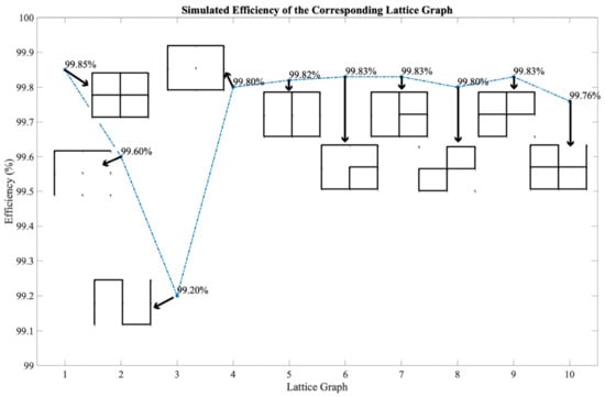
Figure 15.
Simulated efficiencies of corresponding lattice graphs.
Table 3 shows 12 control strategies for the 3 × 3 fully connected lattice converter with different required outputs and starting/destination terminals. It compares the desired output voltages/currents to the simulated outputs, showing their percent difference. The percent difference between the desired and simulated voltages fluctuates around 0.13%. These results indicate that lattice converters are capable of producing the desired outputs, whether positive or negative. Further, they are able to do so with varying input/output ports.
Table 3.
Comparison between desired and simulated output voltages and currents. Load resistance is 10 Ω, internal resistances are 0.01 Ω for all edges.
5. Conclusions
This article proposes a general methodology for control and optimization of lattice converters. While enjoying scalability and versatility, lattice converters suffer from control complexity, thus necessitating algorithms for guiding control and optimization. We begin by introducing two objectives: efficiency optimization and node voltage solution. We then simplify the problems by employing graph theory and representing lattice structures as adjacency matrices. With this tool, we calculate the efficiencies of given lattices and optimize such efficiencies. We further provide the algorithm for finding the voltage at each node, which guides the control of individual edges, or H-bridges. Then, we present examples regarding 3 × 3 and 4 × 4 lattices, showing that with load resistance of 10 Ω and internal resistance of 0.01 Ω, 3 × 3 lattices can achieve a 99.85% efficiency and 4 × 4 lattices can have a 99.81% efficiency. Moreover, we present node voltage solutions to the most efficient 3 × 3 and 4 × 4 lattices and explain the multitude of such solutions. Finally, we simulate the proposed control strategies and verify both efficiency calculations and node voltage solutions. Future works can focus on simplifying lattice efficiency calculations, further classifying node voltage solutions, incorporating different internal resistances for each H-Bridge, considering cases for switch failure, expanding the lattice size, and improving the robustness of the control algorithm. This work sets the ground for efficient and coherent lattice converter designs.
Author Contributions
Conceptualization, J.F., S.G. and Z.M.; methodology, J.F. and Z.M.; software, Z.M. and J.F.; validation, Z.M. and J.F.; formal analysis, Z.M. and J.F.; investigation, Z.M. and J.F.; resources, J.F.; data curation, Z.M. and J.F.; writing—original draft preparation, Z.M.; writing—review and editing, J.F. and S.G.; visualization, Z.M.; supervision, J.F.; project administration, J.F.; funding acquisition, J.F. All authors have read and agreed to the published version of the manuscript.
Funding
This research received no external funding.
Institutional Review Board Statement
Not applicable.
Informed Consent Statement
Not Applicable.
Data Availability Statement
Study did not report any data.
Conflicts of Interest
The authors declare no conflict of interest.
References
- Fang, J.; Blaabjerg, F.; Liu, S.; Goetz, S. A review of multilevel converters with parallel connectivity. IEEE Trans. Power Electron. 2021, 36, 12468–12489. [Google Scholar] [CrossRef]
- Fang, J.; Li, H.; Tang, Y.; Blaabjerg, F. On the inertia of future more-electronics power systems. IEEE J. Emerg. Sel. Top. Power Electron. 2019, 7, 2130–2146. [Google Scholar] [CrossRef]
- Flourentzou, N.; Agelidis, V.G.; Demetriades, G.D. VSC-based HVDC power transmission systems: An overview. IEEE Trans. Power Electron. 2009, 24, 592–602. [Google Scholar] [CrossRef]
- Allebrod, S.; Hamerski, R.; Marquardt, R. New transformerless, scalable modular multilevel converters for HVDC-transmission. In Proceedings of the 2008 IEEE Power Electronics Specialists Conference, Rhodes, Greece, 15–19 June 2008; pp. 174–179. [Google Scholar]
- Lesnicar, A.; Marquardt, R. An innovative modular multilevel converter topology suitable for a wide power range. In Proceedings of the IEEE Bologna Power Tech Conference Proceedings, Bologna, Italy, 23–26 June 2003; p. 3. [Google Scholar]
- Jacobson, B.; Karlsson, P.; Asplund, G.; Harnefors, L.; Jonsson, T. VSC-HVDC transmission with cascaded two-level converters. In Cigré Session; Cigre: Paris, France, 2010; pp. B4–B110. [Google Scholar]
- Villanueva, E.; Correa, P.; Rodriguez, J.; Pacas, M. Control of a single-phase cascaded h-bridge multilevel inverter for grid-connected photovoltaic systems. IEEE Trans. Ind. Electron. 2009, 56, 4399–4406. [Google Scholar] [CrossRef]
- Daher, S.; Schmid, J.; Antunes, F. Multilevel inverter topologies for stand-alone PV systems. IEEE Trans. Ind. Electron. 2008, 55, 2703–2712. [Google Scholar] [CrossRef]
- Ertl, H.; Kolar, J.; Zach, F. A novel multicell DC–AC converter for applications in renewable energy systems. IEEE Trans. Ind. Electron. 2002, 49, 1048–1057. [Google Scholar] [CrossRef]
- Reddi, N.K.; Ramteke, M.R.; Suryawanshi, H.M.; Kothapalli, K.; Gawande, S.P. An isolated multi-input ZCS DC–DC front-end-converter based multilevel inverter for the integration of renewable energy sources. IEEE Trans. Ind. Appl. 2018, 54, 494–504. [Google Scholar] [CrossRef]
- Pouresmaeil, E.; Gomis-Bellmunt, O.; Montesinos-Miracle, D.; Bergas-Jané, J. Multilevel converters control for renewable energy integration to the power grid. Energy 2011, 36, 950–963. [Google Scholar] [CrossRef]
- Choudhury, A.; Pillay, P.; Williamson, S.S. Modified DC-bus voltage-balancing algorithm based three-level neutral-point-clamped IPMSM drive for electric vehicle applications. IEEE Trans. Ind. Electron 2016, 63, 761–772. [Google Scholar] [CrossRef]
- Gan, C.; Sun, Q.; Wu, J.; Kong, W.; Shi, C.; Hu, Y. MMC-based SRM drives with decentralized battery energy storage system for hybrid electric vehicles. IEEE Trans. Power Electron. 2019, 34, 2608–2621. [Google Scholar] [CrossRef]
- Ronanki, D.; Williamson, S.S. Modular multilevel converters for transportation electrification: Challenges and opportunities. IEEE Trans. Transp.Electrif. 2018, 4, 399–407. [Google Scholar] [CrossRef]
- Quraan, M.; Yeo, T.; Tricoli, P. Design and control of modular multilevel converters for battery electric vehicles. IEEE Trans. Power Electron. 2016, 31, 507–517. [Google Scholar] [CrossRef]
- Quraan, M.; Tricoli, P.; Arco, S.D.; Piegari, L. Efficiency assessment of modular multilevel converters for battery electric vehicles. IEEE Trans. Power Electron. 2017, 32, 2041–2051. [Google Scholar] [CrossRef]
- Badawy, M.; Sharma, M.; Hernandez, C.; Elrayyah, A.; Coe, J. Model predictive control for multi-port modular multilevel converters in electric vehicles enabling HESDs. IEEE Trans. Energy Convers. 2021, 1. [Google Scholar] [CrossRef]
- Zheng, Z.; Wang, K.; Xu, L.; Li, Y. A hybrid cascaded multilevel converter for battery energy management applied in electric vehicles. IEEE Trans. Power Electron. 2014, 29, 3537–3546. [Google Scholar] [CrossRef]
- Peng, F.Z.; Lai, J. Dynamic performance and control of a static var generator using cascade multilevel inverters. IEEE Trans. Ind. Appl. 1997, 33, 748–755. [Google Scholar] [CrossRef]
- Peng, F.Z.; Lai, J.; McKeever, J.W.; VanCoevering, J. A multilevel voltage-source inverter with separate dc sources for static var generation. IEEE Trans. Ind. Appl. 1996, 32, 1130–1138. [Google Scholar] [CrossRef] [Green Version]
- Peng, F.Z.; Liu, Y.; Yang, S.; Zhang, S.; Gunasekaran, D.; Karki, U. Transformer-less unified power-flow controller using the cascade multi- level inverter. IEEE Trans. Power Electron. 2016, 31, 5461–5472. [Google Scholar] [CrossRef]
- Shi, J.; Gou, W.; Yuan, H.; Zhao, T.; Huang, A. Research on voltage and power balance control for cascaded modular solid-state transformer. IEEE Trans. Power Electron. 2011, 26, 1154–1166. [Google Scholar] [CrossRef]
- Falcones, S.; Mao, X.; Ayyanar, R. Topology comparison for solid state transformer implementation. In Proceedings of the IEEE PES general meeting, Providence, RI, USA, 25–29 July 2010. [Google Scholar]
- Awal, M.A.; Husain, I.; Bipu, M.R.H.; Montes, O.A.; Teng, F.; Feng, H.; Khan, M.; Lukic, S. Modular Medium Voltage AC to Low Voltage DC Converter for Extreme Fast Charging Applications. Available online: https://arxiv.org/abs/2007.04369 (accessed on 9 January 2022).
- Zhang, L.; Tang, Y.; Yang, S.; Gao, F. Decoupled power control for a modular-multilevel-converter-based hybrid AC-DC grid integrated with hybrid energy storage. IEEE Trans. Ind. Electron. 2019, 66, 2926–2934. [Google Scholar] [CrossRef]
- Maharjan, L.; Inoue, S.; Akagi, H.; Asakura, J. State-of-charge (SOC) balancing control of a battery energy storage system based on a cascade PWM converter. IEEE Trans. Power Electron. 2009, 24, 1628–1636. [Google Scholar] [CrossRef]
- Maharjan, L.; Yamagishi, T.; Akagi, H. Active-power control of individual converter cells for a battery energy storage system based on a multilevel cascade PWM converter. IEEE Trans. Power Electron. 2012, 27, 1099–1107. [Google Scholar] [CrossRef]
- Debnath, S.; Qin, J.; Bahrani, B.; Saeedifard, M.; Barbosa, P. Operation, control, and applications of the modular multilevel converter: A review. IEEE Trans. Power Electron. 2015, 30, 37–53. [Google Scholar] [CrossRef]
- Wang, C.; Peterchev, A.V.; Goetz, S.M. Online switch open-circuit fault diagnosis using reconfigurable scheduler for modular multilevel converter with parallel connectivity. In Proceedings of the 21st European Conference on Power Electronics and Applications (EPE ‘19 ECCE Europe), Genova, Italy, 3–5 September 2019. [Google Scholar]
- Wang, C.; Lizana, F.R.; Li, Z.; Peterchev, A.V.; Goetz, S.M. Submodule short-circuit fault diagnosis based on wavelet transform and support vector machines for modular multilevel converter with series and parallel connectivity. In Proceedings of the IECON 2017—43rd Annual Conference of the IEEE Industrial Electronics Society, Beijing, China, 29 October–1 November 2017. [Google Scholar]
- Li, Z.; Lizana, R.; Yu, Z.; Sha, S.; Peterchev, A.V.; Goetz, S. A modular multilevel series/parallel converter for wide frequency range operation. IEEE Trans. Power Electron. 2019, 34, 9854–9865. [Google Scholar] [CrossRef]
- Li, Z.; Lizana, R.; Peterchev, A.V.; Goetz, S.M. Predictive control of modular multilevel series/parallel converter for battery systems. In Proceedings of the 2017 IEEE Energy Conversion Congress and Exposition (ECCE), Cincinnati, OH, USA, 1–5 October 2017; pp. 5685–5691. [Google Scholar]
- Damian, I.C.; Eremia, M. Performance analysis of a full bridge modular multilevel converter for high voltage DC transmission using various pulse width modulation techniques. In Proceedings of the 9th International Conference on Modern Power Systems (MPS), Cluj-Napoca, Romania, 16–17 June 2021; pp. 1–5. [Google Scholar]
- Goetz, S.M.; Peterchev, A.V.; Weyh, T. Modular multilevel converter with series and parallel module connectivity: Topology and control. IEEE Trans. Power Electron. 2015, 30, 203–215. [Google Scholar] [CrossRef]
- Goetz, S.M.; Li, Z.; Liang, X.; Zhang, C.; Lukic, S.M.; Peterchev, A.V. Control of modular multilevel converter with parallel connectivity—application to battery systems. IEEE Trans. Power Electron. 2017, 32, 8381–8392. [Google Scholar] [CrossRef]
- Fang, J.; Goetz, S.M. Symmetries in power electronics. In Proceedings of the IEEE ECCE, Vancouver, BC, Canada, 10–14 October 2021. [Google Scholar]
- Lizana, R.; Rivera, S.; Li, Z.; Dekka, A.; Rosenthal, L.; Bahamonde, H.; Peterchev, A.V.; Goetz, S.M. Modular multilevel series/parallel converter for bipolar DC distribution and transmission. IEEE J. Emerg. Sel. Top. Power Electron. 2021, 9, 1765–1779. [Google Scholar] [CrossRef]
- Fang, J.; Yang, S.; Wang, H.; Tashakor, N.; Goetz, S.M. Reduction of MMC capacitances through parallelization of symmetrical half-bridge submodules. IEEE Trans. Power Electron. 2021, 36, 8907–8918. [Google Scholar] [CrossRef]
- Ilves, K.; Bessegato, L.; Harnefors, L.; Norrga, S.; Nee, H.-P. Semi-full-bridge submodule for modular multilevel converters. In Proceedings of the 9th International Conference on Power Electronics and ECCE Asia (ICPE-ECCE Asia), Seoul, South Korea, 1–5 June 2015. [Google Scholar]
- Gunasekaran, D.; Yang, S.; Peng, F.Z. A cascaded two-port bridge multilevel converter with automatic voltage balancing capability. In Proceedings of the 2015 IEEE Energy Conversion Congress and Exposition (ECCE), Montreal, QC, Canada, 20–24 September 2015. [Google Scholar]
- Fang, J.; Li, Z.; Goetz, S.M. Multilevel converters with symmetrical half-bridge submodules and sensorless voltage balance. IEEE Trans. Power Electron. 2021, 36, 447–458. [Google Scholar] [CrossRef]
- Xu, J.; Li, J.; Zhang, J.; Shi, L.; Jia, X.; Zhao, C. Open-loop voltage balancing algorithm for two-port full-bridge MMC-HVDC sytem. Int. J. Electr. Power Energy Syst. 2019, 109, 259–268. [Google Scholar] [CrossRef]
- Fang, J. Unfied graph theory-based modeling and control methodology of lattice converters. Electronics 2021, 10, 2146. [Google Scholar] [CrossRef]
Publisher’s Note: MDPI stays neutral with regard to jurisdictional claims in published maps and institutional affiliations. |
© 2022 by the authors. Licensee MDPI, Basel, Switzerland. This article is an open access article distributed under the terms and conditions of the Creative Commons Attribution (CC BY) license (https://creativecommons.org/licenses/by/4.0/).