
Hybrid Converter with Multiple Sources for Lithium Battery Charger Applications


Department of Electrical Engineering, Chang Gung University, Taoyuan 33302, Taiwan
*
Author to whom correspondence should be addressed.
Electronics 2022, 11(4), 616; https://doi.org/10.3390/electronics11040616
Submission received: 30 December 2021
/
Revised: 6 February 2022
/
Accepted: 14 February 2022
/
Published: 16 February 2022
(This article belongs to the Special Issue Electronic Devices on Intelligent IoT Applications)
Abstract
:This paper proposes a hybrid converter with multiple sources for lithium battery charger applications. Since the output voltage of a lithium battery charger is very low, its charger needs a higher step-down voltage for a utility line source or a step-down voltage for PV arrays. In order to implement the battery charger with utility line and PV arrays sources to simultaneously supply power to battery, a flyback converter is selected for utility line sources, and a buck converter is adopted for PV arrays source. Due to leakage inductor of transformer in flyback converter, an active clamp circuit is introduced into flyback converter to recover the energy stored in leakage inductor. In addition, flyback and buck converters can adopt switch integration techniques to simplify circuit structure. With this approach, the proposed hybrid converter has less components, is lighter weight and has smaller size and higher conversion efficiency. Finally, a prototype of the proposed hybrid converter with output voltage of 5 V~8.4 V and output maximum current of 12 A has been implement to verify its feasibility. It is suitable for the lithium battery charger applications.
1. Introduction
Currently, advances in switching power supply technology have created high energy density with lower volume, size and cost. It is widely applied to power systems to generate electric power to load, such as ac/dc converter, dc/dc converter, uninterrupted power supply (UPS), induction heating, electronic ballast, telecom power supplies, light emitting diode drivers and battery charger and dischargers [1,2,3,4,5]. In particular, battery power is rapidly replacing fossil fuel as an energy storage system in a variety of power system application, such as energy storage cabinet system, UPS, electric vehicle, small bikes, garden tools, vacuum cleaners and 3C products [6,7,8,9,10].
In general, battery power is combined with renewable energy sources to generate electric power to load due to zero pollution. In particular, when solar power is regarded as an input power source of power processor, different types of power sources should be merged to transfer less fluctuated and more reliable energy to load due to its intermittent feature. In order to supply power to the battery, a utility line source is selected to help solar power to sustain continuous energy to battery when solar power is functioning with less intense solar radiation. Therefore, solar power sources and utility line sources are simultaneously selected in the proposed power system to increase power reliability for battery charging applications.
When charger is widely used in power systems, various battery types are chosen to achieve storage energy. Since lithium battery possesses high energy density, small size and low self-discharge [11,12,13], it is extensively adopted in portable products. However, the lifetime of lithium battery is easily affected by the charging method. In order to increase life time of lithium battery, many battery charging methods have been proposed [14,15,16]. They include constant trickle current (CTC), constant current (CC) and constant current/constant voltage (CC-CV) charging methods. In these methods, since CTC charging method requires a longer charging time, its applications are limited. Since the CC-CV charging method can reduce charging time, it is suitable for the utility line source system. In addition, battery charger adopts solar power as it input source. To implement maximum power point tracking (MPPT) of solar power, the CC charging method can be used to extract its maximum power. Therefore, CC-CV and CC charging methods are, respectively, adopted in the proposed power system operated in the utility line and solar power source conditions.
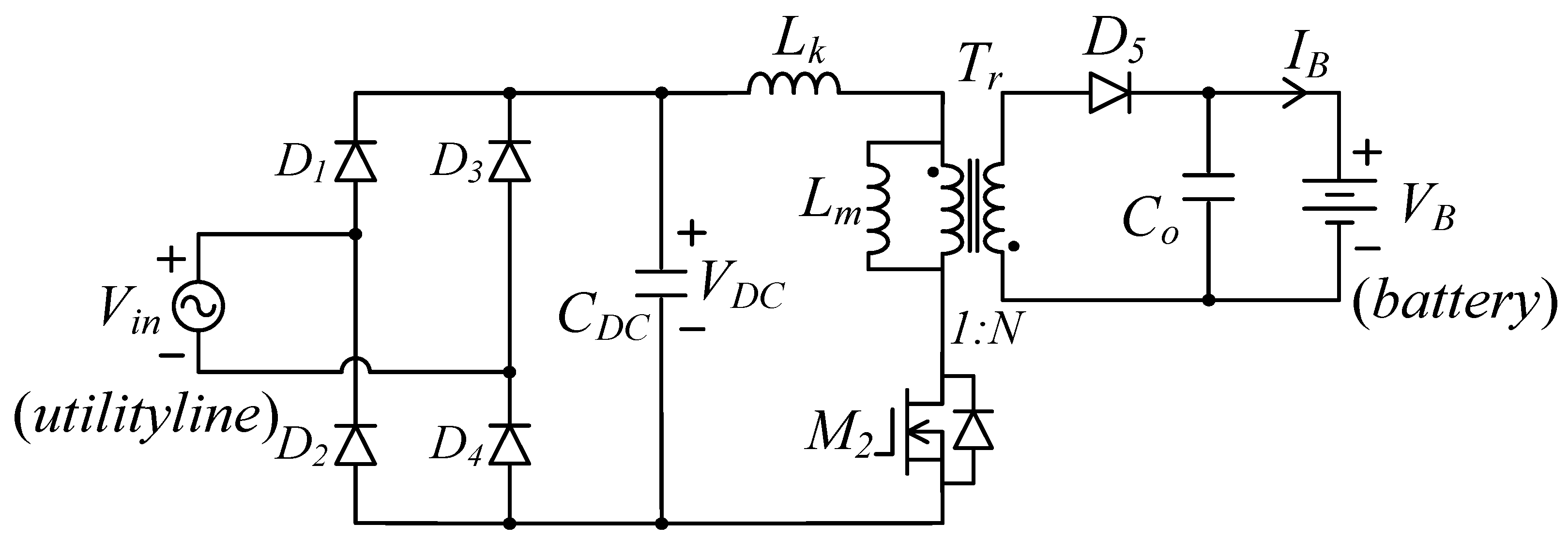
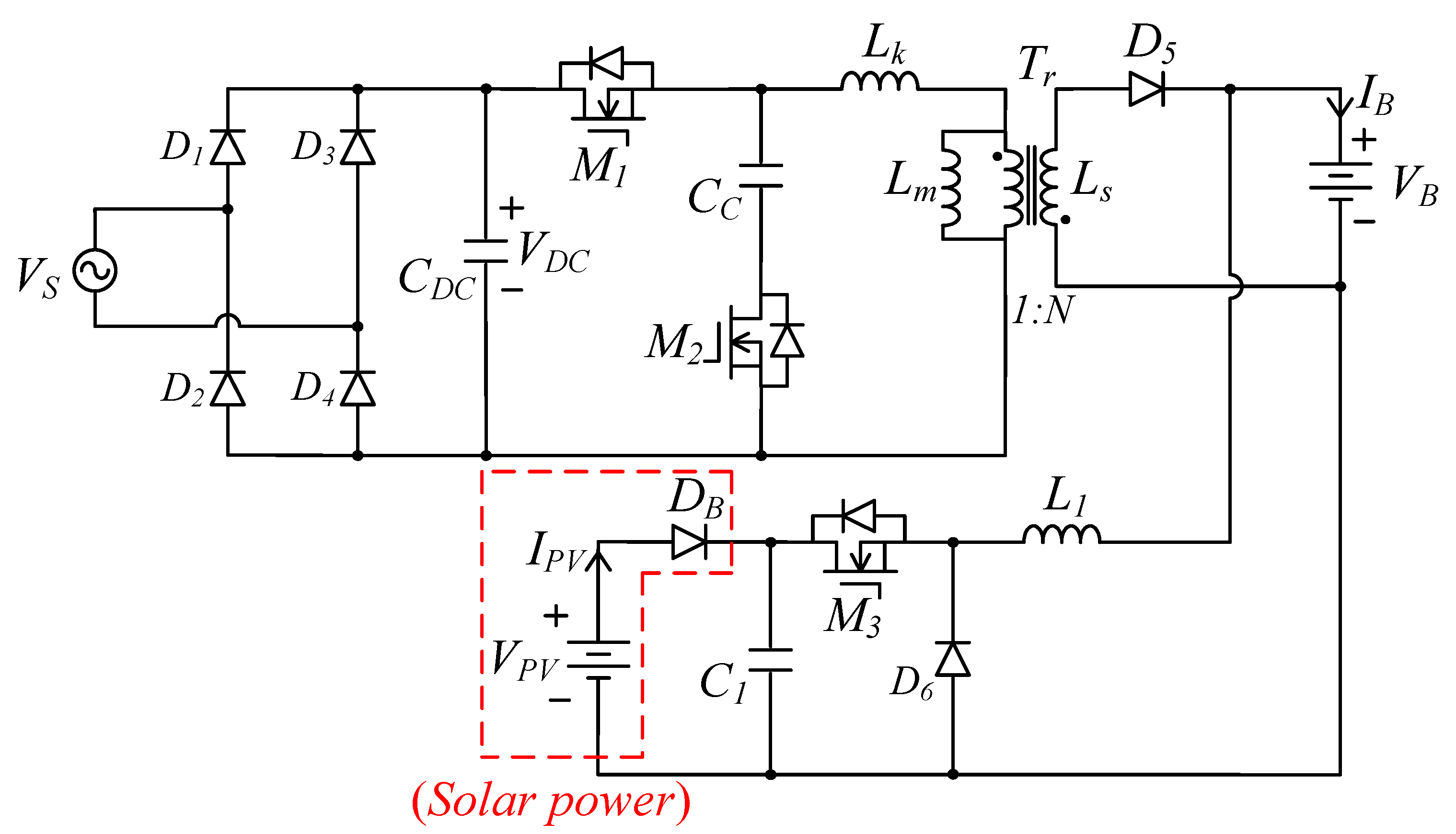
In general, a battery cell is connected in series or parallel to form a battery pack for power system applications. Since a battery pack uses a lot of battery cells connected in series, it will result in voltage difference between each battery cell. Therefore, the lifetime and maximum storage capacity of battery pack can be reduced. In order to obtain better lifetime and maximum storage capacity of the battery, a battery pack with two or three battery cells connected in series is usually adopted without a battery equalizer. Its output voltage is less than 13 V. When a battery charger uses the utility line source as its input source, it needs a high step-down converter. Due to the low-level power application of the proposed charger, a flyback or forward converter can be selected as the charging converter. Moreover, a flyback converter has a better circuit and costs less. It is regarded as the charger when the proposed power system is operated in the utility line source condition, as shown in Figure 1. If the proposed one adopts solar power as its input source, a buck converter can be chosen as the charger because of low voltage differences between the output voltage of solar power and the battery, as shown in Figure 2. Therefore, the proposed power system operated in the utility line source condition adopts a flyback converter as its charger, while the proposed one operated in the solar power source condition uses a buck converter as its charger.
The proposed power system can select flyback and buck converters to achieve multiple sources for lithium battery charger applications, as shown in Figure 3. Since transformer Tr in flyback converter exists with leakage inductance LK, it will induce a spike voltage across switch M1 when switch M1 is switched off. In order to recover the energy trapped in leakage inductance LK, an active clamp circuit is introduced into the flyback converter to increase conversion efficiency [17,18,19,20]. Moreover, a buck converter can adopt a bidirectional circuit to implement the battery charger. For further simplifying circuit topology of the proposed power system, switches of active clamp flyback and bidirectional buck converters can be merged to form a hybrid converter, as shown in Figure 4. In Figure 4, since the utility line source and solar power source conditions are separately operated and their exchange time is very long, switch S1 with a low speed and low cost is adopted to control operational conditions. In addition, the proposed hybrid converter can use less components and is of lighter volume, smaller size, lower cost and higher conversion efficiency. It is suitable for battery charger systems with multiple sources, such as Ni-Cd, Ni-MH, lead-acid, lithium batteries, etc.
The multiport converter has been widely applied to generate electric power [21,22,23,24,25,26]. In [21], a multi-port converter was used in smart grid for the integration of storage and distributed generator. The authors of [22] proposed a multi-input dc-dc converter to transfer power from different power sources to the load. In order to implement input source of converter with multiple power sources, their component counts were added, and their driving circuits are complex. In [23,24,25,26], they are adopted in PV and battery system for supplying power to load. They possess dual input and single output ports. The proposed hybrid converter is shown in Figure 4. It is similar to three-port converter: dual inputs and single output. Comparison of component counts with the proposed hybrid converter and its counterparts is illustrated in Table 1. From Table 1, it can be observed that the proposed one can implement dual inputs and single output. It only uses one transformer, three switches, one capacitor and one extra switch. Compared with its counterparts, the proposed hybrid converter can reduce component counts to achieve approximately functions.
2. Derivation of the Proposed Hybrid Converter
Since the proposed hybrid converter includes an active clamp flyback and buck converter for battery charging applications, illustrated in Figure 3, it will become a complex circuit structure. In Figure 3, the active clamp flyback and buck converters are operated at different times, and the operational time of each converter is very long. Therefore, two sets of converters can be integrated as a hybrid converter. In the following, a circuit structure derivation is briefly described.
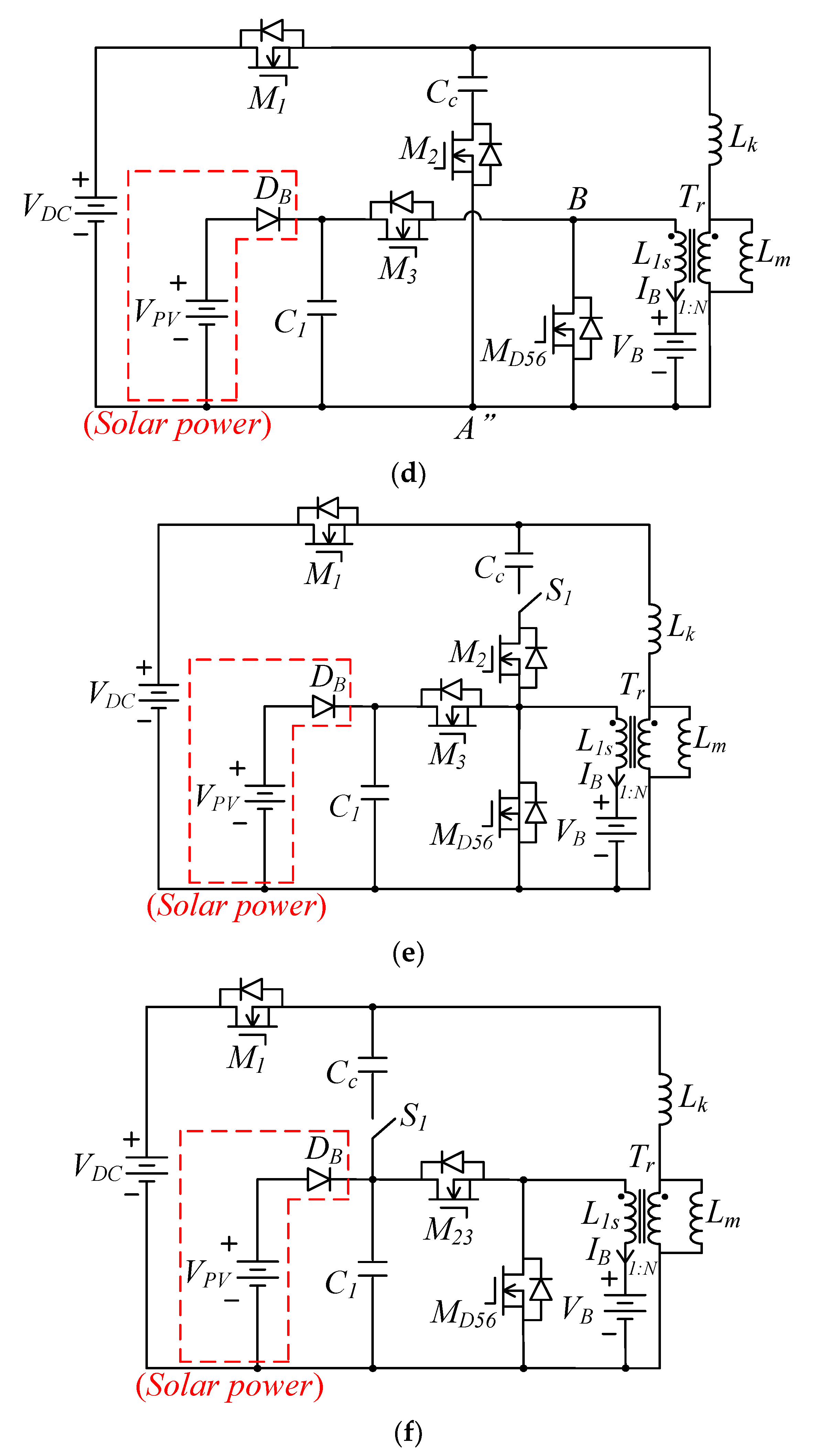
In order to simplify circuit structure of the proposed hybrid converter, diodes D5 and D6 shown in Figure 3 are, respectively, changed by switches MD5 and MD6 illustrated in Figure 5a. In Figure 5a, when switch MD5 is moved from the upper regions to the lower loop, which consists of switch MD5, voltage VB and inductor LS, the operation of the proposed power system is not affected, as shown in Figure 5b. If switches MD5 and MD6 are operated synchronously, two switches can be merged by switch MD56. Moreover, inductors L1 and LS can be integrated to form inductors L1S, as shown in Figure 5c.
In order to further simplify the proposed power system, nodes A and A’ are regarded as the same node AA’. Its circuit structure is illustrated in Figure 5d. When the operational condition of the proposed one is operated in the flyback converter condition, switches M2 and MD56 are switched on or switched off at the same time. Therefore, the S terminal of switch M2 connected in node AA’ can be moved to node B. The operation of the proposed one is not affected, as shown in Figure 5e. Since flyback and buck converters are operated at different times and their exchange time is very long, switch S1 with low speed and low cost can be used to control the operational condition of the proposed power system. Therefore, switches M2 and M3 are integrated to form switch M23, as shown in Figure 5f. To simplify component symbol, the component devices of the proposed hybrid converter are renamed, as shown in Figure 4. From Figure 4, it can be observed that proposed hybrid converter can use less component counts to implement battery charger under utility line and solar power sources.
3. Operational Principle of the Proposed Hybrid Converter
The proposed hybrid converter can be operated in the utility line source and solar power source conditions for lithium battery charging applications. When the proposed one is operated in the solar power source condition, its equivalent circuit is illustrated in Figure 6a by the blue line. Figure 6b shows equivalent circuit of the proposed one operated in the utility line source condition by the blue line. In order to explain the operational principle of the proposed one, each converter is briefly described in the following.
- A.
- The solar power source condition: buck converter
When the proposed hybrid converter is operated in the solar power source condition, its equivalent circuit is shown in Figure 6a. Its equivalent circuit is a buck converter. Since the operational state of the proposed converter is always in continuous conduction mode (CCM) from light load to heavy load, its operational principle with CCM is briefly described. According to the operational principle of the proposed converter operated in the solar power source condition, its operational principle can be divided into five modes. Figure 7 illustrates an equivalent circuit of each operational mode by the blue line. While Figure 8 shows conceptual waveforms of each operational mode over a complete switching cycle. In the following, each operational mode is briefly explained.
Mode 1 (Figure 7a: t0 ≤ t < t1): Before t0, switches M2 and M3 are in the off state. Diode DM3 is in the forward bias state. When t = t0, switch M2 is switched on. Since switch current IDS3 is equal to (–IB), switch current IDS2 abruptly increases from 0 A to IB. Therefore, diode is DM3 reversely biased. During this time interval, current IB linearly increases and inductor Ls is in the storage energy state.
Mode 2 (Figure 7b: t1 ≤ t < t2): At t1, switch M2 is switched off and switch M3 is kept in the off state. Within this time interval, since inductor current IB has to be sustained at continuous state, capacitor CM2 is operated in the charging state, while CM3 is sustained in the discharging state. Therefore, voltage VDS2 varies from 0 V to VPV and voltage VDS3 changes from VPV to 0 V.
Mode 3 (Figure 7c: t2 ≤ t < t3): When t = t2, switches M2 and M3 are kept in the off state. At the moment, voltage VDS3 is equal to 0 V. Diode DM3 is forwardly biased. During this time period, inductor Ls is in the released energy state. Its current, IB, linearly decreases.
Mode 4 (Figure 7d: t3 ≤ t < t4): At t = t3, switch M2 is in the off state and M3 is switched on. Since diode DM3 is forwardly biased before t = t3, switch M2 is operated with zero-voltage switching (ZVS) at the turn-on transition. During this time interval, inductor LS releases energy to the battery. Its current, IB, linearly decreases.
Mode 5 (Figure 7e: t4 ≤ t < t5): When t = t4, switch M2 is in the off state and M3 is switched off. Within this mode, switch current IDS3 is a negative value. Diode DM3 is forwardly biased to release energy stored in inductor Ls to the battery. Inductor current IB linearly decreases. When the operational mode is at the end of mode 5, one new switching cycle will start.
- B.
- The utility line source condition: active clamp flyback converter
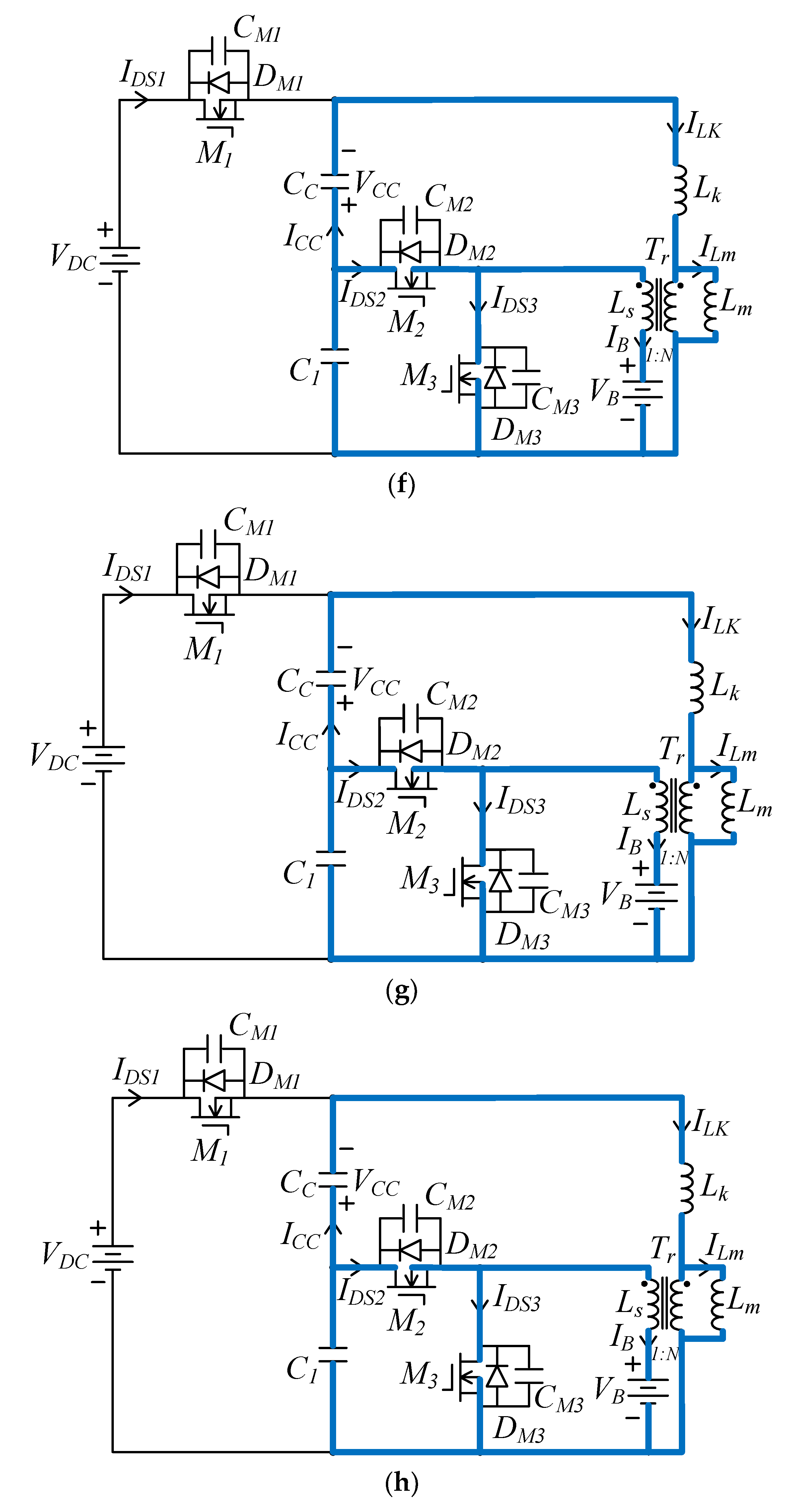
When the proposed hybrid converter is operated in the utility line source condition, an active clamp flyback converter is used to charge battery. Since the operational state of active clamp flyback converter is always kept in CCM from light load to heavy load, the operational principle of the one is briefly described for CCM operation. According to the operational principle of active clamp flyback converter, its operational mode can be divided into 10 modes. The equivalent circuit of each operational mode is shown in Figure 9 by the blue line, while the conceptual waveforms of each operational mode is illustrated in Figure 10. In the following, each operational mode is briefly explained.
Mode 1 (Figure 9a: t0 ≤ t < t1): Before t0, switches M1~M3 are in the off state, and diodes DM1 and DM1 are in the forwardly bias state. When t = t0, switch M1 is switched on, and switches M2 and M3 are kept in the off state. At the moment, since diode DM1 is forwardly biased before t0, switch M1 is operated with ZVS at turn-on transition. During this time interval, current ILK varies from a negative value to 0 A. Since current IDS3 is a negative value, diode DM3 is in the forwardly bias state. Current IB linearly decreases and inductor Lm releases energy through transformer Tr and diode DM3 to the battery.
Mode 2 (Figure 9b: t1 ≤ t < t2): At t1, switch M1 is kept in the on state, and switches M2 and M3 are sustained in the off state. Within this mode, inductor current ILK varies from 0 A to the initial value, which is the maximum inductor current of inductor Lm operated in CCM. Moreover, since current IDS3 is kept at the negative value, diode DM3 is sustained in the forwardly bias state. The magnetizing inductor Lm releases energy to battery.
Mode 3 (Figure 9c: t2 ≤ t < t3): When t = t2, switch M1 is sustained in the on state, and switches M2 and M3 are in the off state. At the moment, inductor current ILK is equal to current ILm. Diode DM3 is reversely biased. During this time interval, inductor Lm is in the storage energy state. Inductor current ILm linearly increases.
Mode 4 (Figure 9d: t3 ≤ t < t4): When t = t3, switch M1 is switched off, and switches M2 and M3 are kept in the off state. During this time interval, since inductor current ILK has to be kept in the continuous state, capacitor CM1 is charged, and capacitors CM2 and CM3 are simultaneously discharged. Therefore, voltage VDS1 varies from 0 V to [VDC + NVB]. Voltage VDS3 changes from [(VDC/N) + VB] to 0 V, while voltage VDS2 varies from [(N-1)VB +(N-1)VDC/N] to 0 V.
Mode 5 (Figure 9e: t4 ≤ t < t5): At t4, switch M1~M3 are kept in the off state. In this moment, voltages VDS2 and VDS3 are equal to 0 V. Diode DM2 and DM3 are forwardly biased, simultaneously. During this time interval, inductor LK and capacitor CC form a resonant network, and they start to generate resonance. Inductor current ILm releases energy through transformer Tr and diode DM3 to battery. ILm linearly increases.
Mode 6 (Figure 9f: t5 ≤ t < t6): When t = t5, switch M1 is sustained in the off state, while switches M2 and M3 are simultaneously switched on. At the moment, switches M2 and M3 are simultaneously operated with ZVS at the turn-on transition. Within this mode, inductor LK and capacitor CC are sustained in the resonant state. Current ILK with the resonant manner varies from a maximum negative value to 0 A. Inductor Lm is kept in the released energy state. Therefore, inductor current ILm linearly increases.
Mode 7 (Figure 9g: t6 ≤ t < t7): When t = t6, switch M1 is in the off state and switches M2 and M3 are kept in the on state. In this moment, current ILK is equal to 0 A. During this time interval, inductor LK and capacitor CC are sustained in the resonant state. Inductor Lm releases energy through transformer Tr and switch M3 to the battery. Therefore, inductor current ILm linearly increases. Since switch current IDS3 is equal to (IB–IDS2), it varies from a negative value to 0 A.
Mode 8 (Figure 9h: t7 ≤ t < t8): At t7, switch M1 is kept in the off state, while switches M2 and M3 are simultaneously sustained in the on state. Within this mode, Inductor LK and capacitor CC are kept in the resonant state. Inductor current ILK with the resonant manner varies from 0 A to the maximum value. Inductor Lm is in the released energy state. Its value linearly increases.
Mode 9 (Figure 9i: t8 ≤ t < t9): When t = t8, switch M1 is in the off state, while switches M2 and M3 are simultaneously switched on. In this mode, current IDS3 is equal to (−IB). Diode DM3 is forwardly biased. Since inductor current ILK must be kept in the continuous state, capacitor CM1 is discharged, and capacitor CM2 is charged. Voltage VDS1 varies from [VDC + NVB] to 0 V, while voltage VDS2 changes from 0 V to [(N − 1)VB +(N − 1)VDC/N]. Inductor Lm is kept in the released energy state.
Mode 10 (Figure 9j: t9 ≤ t < t10): At t = t9, switch M1 ~ M3 are in the off state. At the moment, voltage VDS1 is equal to 0 V. Thus, diode DM1 is forwardly biased. During this time interval, inductor current ILK varies from the maximum negative value to 0 A. Inductor current Lm is still in the released energy state. When operational mode is at the end of mode 10, one new switching cycle will start.
4. Design of the Proposed Hybrid Converter
Design of the proposed hybrid converter can be divided into two conditions. One is the utility line source condition, and the other is the solar power source condition. In the following, the design of each operational condition is briefly derived.
4.1. The Utility Line Source Condition: Active Clamp Flyback Converter
When the proposed hybrid converter is operated in the utility line source condition, the active clamp flyback converter is adopted to charge lithium battery. Its key parameter design is analyzed in the following.
4.1.1. Duty Ratio D11
Since the active clamp flyback converter does not affect design of duty ratio D11 and transformer Tr, the designs of D11 and transformer Tr are the same as the conventional flyback converter. According to volt-second balance of magnetizing inductance Lm, the relationship between voltage VDC and output voltage VB can be expressed as follows:
where N is turns ratio of transformer Tr, VDC represents the equivalent dc voltage of utility line and Ts expresses the period of switching cycle. From (1), the conversion ratio M11 of the active clamp flyback converter can be indicated by the following.
When input voltage VDC and battery voltage VB are specified, duty ratio D11 can be rewritten as follows.
In (3), when N is kept at a constant value, the maximum duty ratio D11(max) is determined under the maximum battery voltage VB(max) and minimum input voltage VDC(min). That is, the maximum duty ratio D11(max) is determined by the following.
In general, if the maximum duty ratio of a pulse-width modulation integrated circuit (PWM IC) is limited within 0.5, the maximum duty ratio D11(max) has better selection ranges from 0.35 to 0.4.
4.1.2. Transformer Tr
For the design of transformer Tr, turn ratio N and magnetizing inductance Lm are two key parameters. In (4), when the maximum duty ratio D11(max), battery voltage VB(max) and input voltage VDC(min) are determined, turns ratio N can be rewritten by the following.
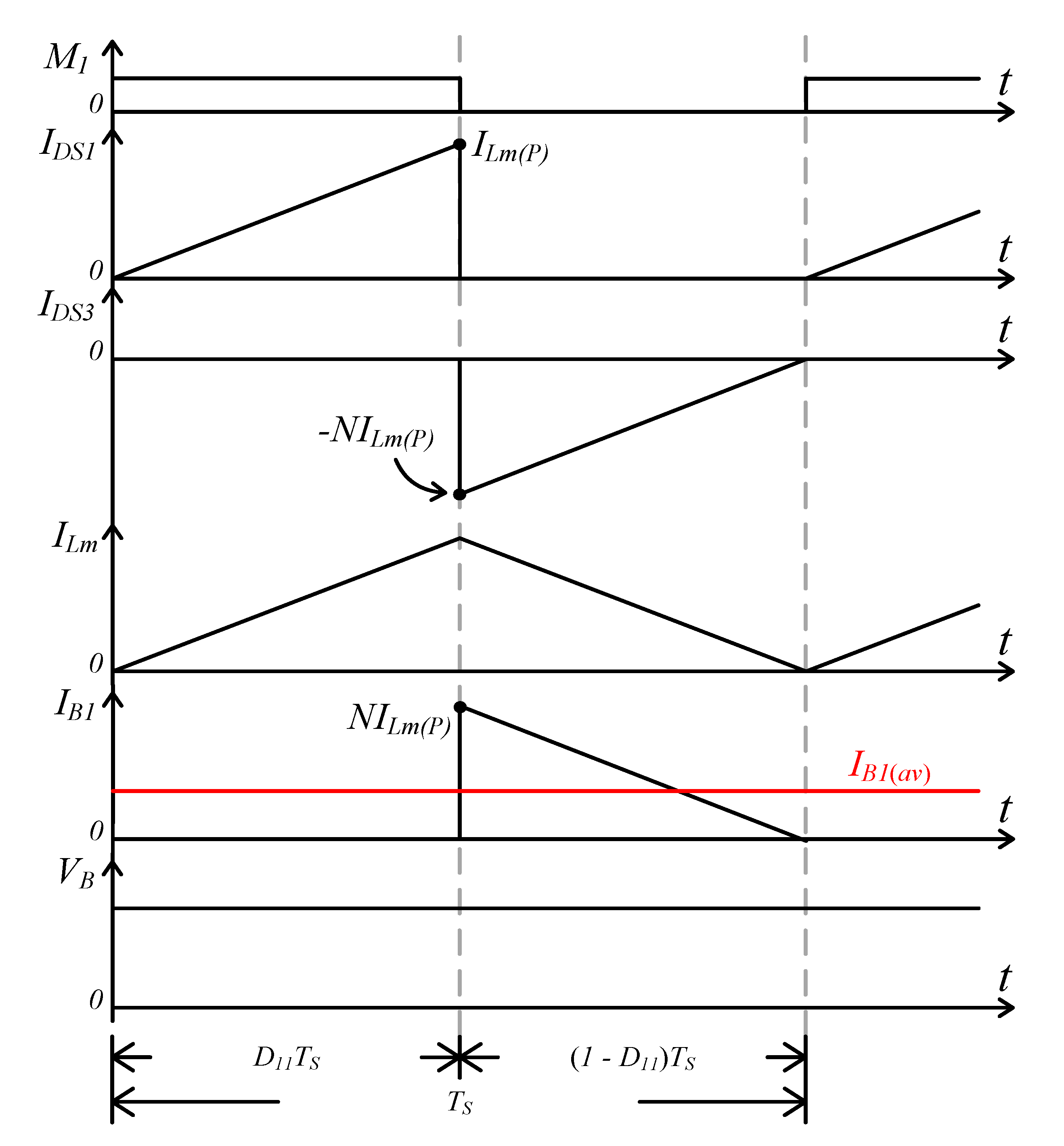
In order to design magnetizing inductance Lm, magnetizing inductor current variation ΔILm1 must be determined. In general, when the proposed flyback converter is operated in the boundaries of CCM and discontinuous conduction mode (DCM), average current IB1(av) can be obtained as the desired reference value. Ratio K1 of the average current IB1(av) to the maximum charging current IB(max) is set. That is, when the proposed converter begins to enter CCM operation, the average current IB1(av) is equal to K1IB(max), where K1 varies from 0 to 1. Figure 11 plots ideal waveforms of inductor current ILm and charging current IB1 of the proposed one operated at the boundary condition. In Figure 11, the average current IB1(av) is expressed by the following.
In Figure 11, current variation ΔILm1 is equal to ILm(P). According to operational principle of the proposed flyback converter, current variation ΔILm1 can be derived as follows:
where LmB1 is the boundary value of magnetizing inductance Lm1 when the proposed flyback converter is operated in the boundary of CCM and DCM. Since the proposed one adopts the active clamp circuit to achieve ZVS operational features under CCM condition, it magnetizing inductance Lm1 is always operated in CCM to increase soft-switching operational ranges. In order to achieve a variety of soft-switching operational ranges, the proposed one begins to enter CCM under light load conditions. From (6) and (7), the magnetizing inductance Lm1 can be expressed as follows.
4.1.3. Capacitor Cc
In the active clamp flyback converter, capacitor Cc is adopted to recover energy stored in leakage inductance LK and achieve ZVS features of switches. Since inductor LK and capacitor Cc are connected in series to form a resonant network, half of the resonant period is equal to or greater than the turn-off time of switch M1 to produce a wider range of soft-switching features. Thus, capacitor Cc has to satisfy the following inequality.
In (9), capacitor Cc can be rewritten as follows.
From (5) and (8), magnetizing inductor Lm1 and turn ratio N of transformer Tr can be obtained, and then the turns of primary and secondary windings of transformer Tr can be determined. According to the turns of primary and secondary windings relative to wind transformer Tr, leakage inductance LK can be measured by the practical wound transformer Tr. When leakage inductance LK is obtained, capacitor Cc can be also determined by (10).
4.2. The Solar Power Source Condition: Buck Converter
When a battery uses solar power as its input source, the buck converter is regarded as the battery charger, as shown in Figure 6a. To design the proposed buck converter, the key parameters are derived in the following.
4.2.1. Duty Ratio D12
In Figure 6a, switch M2 is regarded as the main switch of the proposed buck converter, while switch M3 is used as the auxiliary switch. According to volt-second balance of inductor Ls, its relationship is expressed by the following:
where VPV is output voltage of solar power, VB represents battery voltage and Ts expresses the period of switching cycle. Conversion ratio M12 of the proposed buck converter can be analyzed as follows.
From (12), the maximum duty ratio D12(max) happens at the maximum battery voltage VB(max) and minimum voltage VPV(min). Therefore, the maximum duty ratio D12(max) can be determined by the following.
When the proposed hybrid converter is operated in the solar power condition, the proposed one can regulate output current with CC method to charge lithium battery and extract maximum output power of solar power. Its duty ratio D12 is limited within D12(max), as illustrated in (13).
4.2.2. Inductor Ls
Inductor Ls is the inductance of secondary winding of transformer Tr. Its value is equal to (Lm1/N2). Figure 12 shows ideal waveforms of current IDS2, IDS3 and IB2 of the proposed buck converter operated in the boundaries of CCM and DCM. From Figure 12, the average charging current IB2(av) can be derived by the following:
where ΔILS is the current variation of inductor Ls, and ILS(P) expresses the peak current of inductor Ls. Since voltage VLS across inductor Ls is equal to (VPV – VB) during switch M2 in the on state, current ILS(P) can be the inductor as follows:
where LSB is the boundary inductance of LS when the proposed converter is operated in the boundary of CCM and DCM. In (13), when the maximum voltage VB(max) and minimum voltage VPV(min) are specified, the maximum duty ratio D12(max) can be obtained. Therefore, inductor current ILS(P) can be rewritten as follows.
From (14) and (15), the average current IB2(av) is as follows.
When the proposed buck converter is operated in the boundary, average current IB2(av) is set at K2IB(max), where K2 varies from 0 to 1, and IB(max) expresses the maximum charging current. In general, K2 has a better selection range under 0.2~0.3. Therefore, inductor Ls can be expressed by the following.
Since inductor Ls is equal to (Lm2/N2), inductor Lm2 can be indicated by the following.
In order to design the proposed hybrid converter, inductor Lm of transformer Tr can be determined by inductors Lm1 and Lm2. It can be selected with the larger value between Lm1 and Lm2.
5. Control Circuit of the Proposed Hybrid Converter
The proposed hybrid converter adopts the utility line and solar power as its input source, respectively. In order to achieve a power supply system with multiple sources, the proposed one needs a controller to implement battery charging control and MPPT functions. Figure 13 illustrates the block diagram of the controller for the proposed hybrid converter. In Figure 13, the proposed one is divided into two parts: power circuit and controller. The controller is used to control power circuit for supplying power to battery. Therefore, the controller includes MPPT, power source selection, CC command selection, CC/CV command, PWM generator and battery protection units. Table 2 lists definitions of key parameters in Figure 13, while Table 3 illustrates the operational condition of the proposed hybrid converter. In the following, each control unit is briefly described.
5.1. MPPT Unit
The proposed hybrid converter possesses two operational conditions: the utility line source and solar power source conditions. When the proposed one uses solar power as its input source, it regulates charging current IB with the CC method to charge the battery and implement MPPT. For implementing MPPT of solar power, the perturb and observe algorithm (P&O) was used for tracking the maximum power point (MPP) of solar power [27]. Since its algorithm is described in [27], it will not be described in this paper. As mentioned above, the MPPT unit in the controller adopts voltage VPV and current IPV to obtain the maximum power PPV (max) of solar power.
5.2. CC Command Selection Unit
When the proposed hybrid converter is operated for a battery charger, charging current IB uses the CC-CV method to supply power to the battery. In order to implement the battery charging function with the CC method, the controller must generate CC command value IBCOM to regulate charging current IB. The CC command selection unit is used to generate CC command value IBCOM. When the maximum power PPV(max) of solar power is obtained, the solar power command can produce a command value IBCOM1, which can be expressed by (PPV(max)/VB). Since the charging current IB is limited within IB(max), charging the current selector can generate control signal SCC, which is obtained by the relationship between IBCOM1 and IB(max). When IBCOM1 ≥ IB(max), signal SCC varies from low levels to high levels. It is used to control the CC command selector, and signal IBCOM is equal to IB(max). If IBCOM1 < IB(max), signal SCC is kept at low levels. It can control CC command selector to obtain IBCOM = IBCOM1.
Since the battery charging method adopts the CC–CV hybrid method to obtain better charging efficiency, the CC/CV command unit can produce a selecting signal SCm to control the battery charger operated in the CC charging mode or the CV charging mode. When voltage VB is equal to or greater than voltage VB(max), signal SCm varies from low levels to high levels. The proposed battery charger is operated in the CV charging mode. The command value Vref is equal to VB(max). Moreover, the feedback selector can induce feedback signal Vf, which is equal to VB. The error value can be obtained by difference between the command value Vref and feedback value Vf when signals Vref and Vf are sent to PWM generator for generating error value. The error value compared with a triangle wave in the PWM generator can produce signal SPWM to drive switches in the proposed hybrid converter for battery charging. In addition, when VB < VB(max), the proposed one is operated in the CC charging mode. Signal Vref = IBCOM and Vf = IB. PWM generator can receive signals Vref and Vf to generate SPWM for battery charging.
5.3. PWM Generator Unit
The PWM generator unit includes a feedback selector, PWM generator, gate driver under utility line source, gate driver under solar power source and PWM signal selector. The feedback selector and PWM generator receives command value Vref and feedback value Vf to generate PWM signal SPWM for implementing CC or CV charge. The PWM signal SPWM can be sent to gate driver under utility line source and gate driver under solar power source for generating different PWM signals under different power source to implement battery charger.
In the gate driver under utility line source, the PWM signal SPWM is sent to this control circuit to generate three PWM signals. The PWM signal M11 is used to drive switch M1, which is regarded as the main switch. PWM signals M11 and M12 are operated in complementary, while PWM signals M12 and M13 are operated synchronously. Switches M2 and M3 are regarded as auxiliary switches and are driven by PWM signals M12 and M13, respectively. In addition, the gate driver under the solar power source can produce three PWM signals, M21, M22 and M23, by PWM signal SPWM. PWM signal M22 is the main PWM signal for driving switch M2. The PWM signals M22 and M23 are operated complementarily. Therefore, PWM signal M23 is used to drive auxiliary switch M3. In this operational condition, signal M21 is switched off. Two pairs of PWM signals (M11, M12, M13) and (M21, M22, M23) are sent to a PWM signal selector to produce PWM signals selector to produce PWM signals M1, M2 and M3. When operational signal PSP is in the high level, PWM signals, M1 = M11, M2 = M12, M3 = M13, are adopted to drive switches M1, M2 and M3, respectively. During this operational condition, the proposed hybrid converter is operated in the solar power source condition. Switch S1 is switched off. If operational signal PUL is in the high level, PWM signals M1 = M21, M2 = M22 and M3 = M23 are used to drive switches M1, M2 and M3 separately. Within this operational condition, utility line source is regarded as the input source of the proposed hybrid converter. Switch S1 is switched on. Moreover, signal SD is the shutdown signal of the proposed hybrid converter. When signal SD is in the high level, the proposed one enters the shutdown condition. During this time interval, battery operational condition is under IB ≥ IBP or VB ≥ VBP.
5.4. Power Source Selection Unit
A power source selection unit is used to select power source as input source of the proposed hybrid converter. When solar power can supply enough power to battery, the proposed one can use solar power to supply power for the battery. During this operational condition, the solar power detector is in the VPV ≥ VPV(min) condition. Signal SPV is in the high level. Therefore, signal PSP is under the high level, and signal PUL is in the low level. If VPV ≥ VPV(min) and VDC ≥ VDC (min), signals SPV and SDC are simultaneously in the high level. When VPV ≥ VPV(min) and VDC ≥ VDC (min), signals SPV and SDC are simultaneously in the high level. Within this operational condition, the powers of solar power and utility line are large enough to supply power to battery. Since the power source in the proposed hybrid converter is a priority selection to solar power, the proposed one is operated in the solar power condition. Signal PSP is in the high level state. In addition, when VPV < VPV(min) and VDC ≥ VDC (min), solar power is not enough to supply power to the battery, and the utility line is large enough to supply power to battery. Therefore, a utility line can supply power to the battery. Signal PUL is in the high level state. When VPV < VPV(min) and VDC < VDC (min), solar power and utility lines are not enough to supply power to battery, simultaneously. Signals PSP and PUL are under the low level state. The proposed hybrid converter is operated in the shutdown condition. The operational condition of the proposed one is listed in Table 3.
5.5. Battery Protection Unit
The battery does not operate in overcurrent and overvoltage conditions. When IB ≥ IBP, the charging current IB is greater than the maximum charging current IB(max). Signal SDI is in the high level state, and the proposed hybrid converter must be shut down. If VB ≥ VBP, battery voltage VB is greater than maximum charging voltage VB(max). Signal SDV is in the high level state, and the proposed one can be shut down. Therefore, shutdown signal SD is equal to SDI + SDV. When signal SD is in the high level state, the proposed hybrid converter is operated in the shutdown condition.
6. Experimental Results
The proposed hybrid converter can be operated in the utility line source and solar power source conditions. In order to verify battery charging features, a prototype was implemented with the following specifications:
A. The utility line source condition: active clamp flyback converter
- Input voltage VDC: DC127~183 V (AC90 V~130 V);
- Switching frequency fs1: 50 kHz;
- Output voltage VB: DC5 V~8.4 V (battery pack: 2 series*8 parallel);
- Maximum charging current IB(max): 12 A.
B. The solar power source condition: buck converter
- Input voltage VPV: DC30~45 V (solar panel: PPV(max) = 100 W);
- Switching frequency fs2: 50 kHz;
- Output voltage VB: DC5 V~8.4 V (battery pack: 2 series*8 parallel);
- Maximum charging current IB(max): 12 A.
According to the previous specifications of the proposed hybrid converter operated in different power source conditions, the specifications of solar power is illustrated in Table 4, from which it can be observed that maximum output power PPV(max) = 100 W, maximum power voltage VPV = 36 V and maximum power current IPV = 2.78 A. In addition, the battery pack includes 16 sets of battery cells. Specifications of each battery cell are illustrated in Table 5. Two battery cells connected in series are regarded as a string. Eight sets of strings compose battery pack. In Table 5, the voltage of the battery pack varies from 5 V to 8.4 V, and the maximum charging current IB(max) is equal to 12 A. Therefore, the battery pack is expressed by two series*8 parallel.
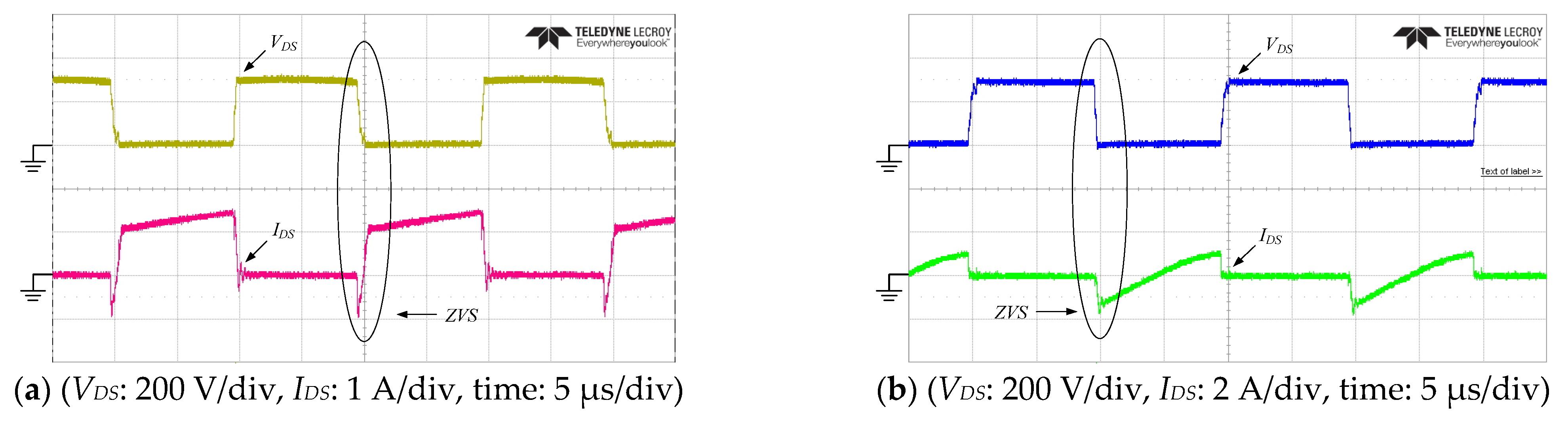
According to the design of the proposed hybrid converter, the key components are listed in Table 6. In order to verify the performances of the proposed hybrid converter, the experimental results are separately measured under solar power and utility line conditions. When solar voltage PPV = 36 V, the measured switch voltage VDS and current IDS waveforms of switches M2 and M3 are shown in Figure 14 and Figure 15. Figure 14 shows those waveforms under 25% of the full-load condition, while Figure 15 depicts those waveforms under 100% of the full-load condition. From Figure 14 and Figure 15, it can be observed that the proposed hybrid converter can adopt solar power to charge battery from light load to heavy load. Figure 16 illustrates measured battery voltage VB and current IB waveforms under different charging currents. When charging current IB = 3 A, those waveforms are shown in Figure 16a. In addition, when IB = 6 A, those waveforms are expressed in Figure 16b. From measured voltage VB and current IB waveforms, the proposed hybrid converter operated in the solar power condition can achieve different charging currents under a constant value.
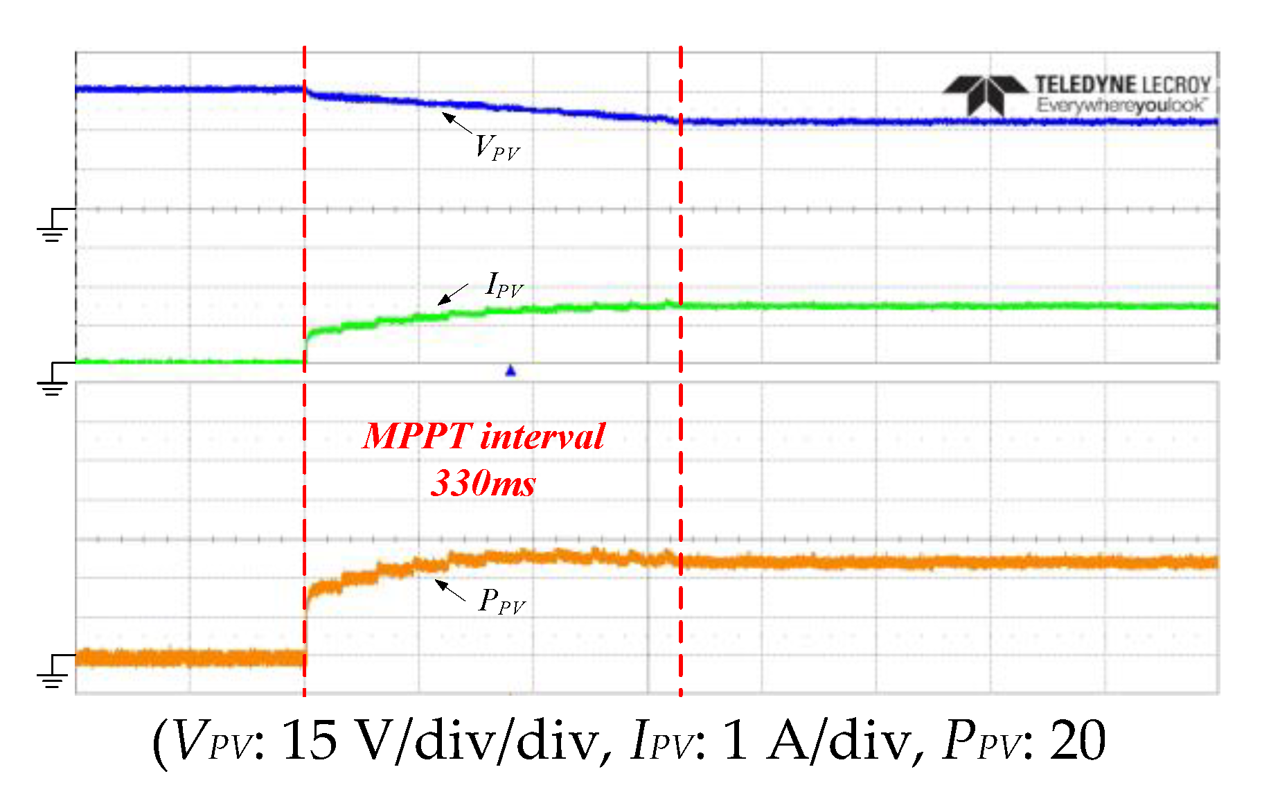
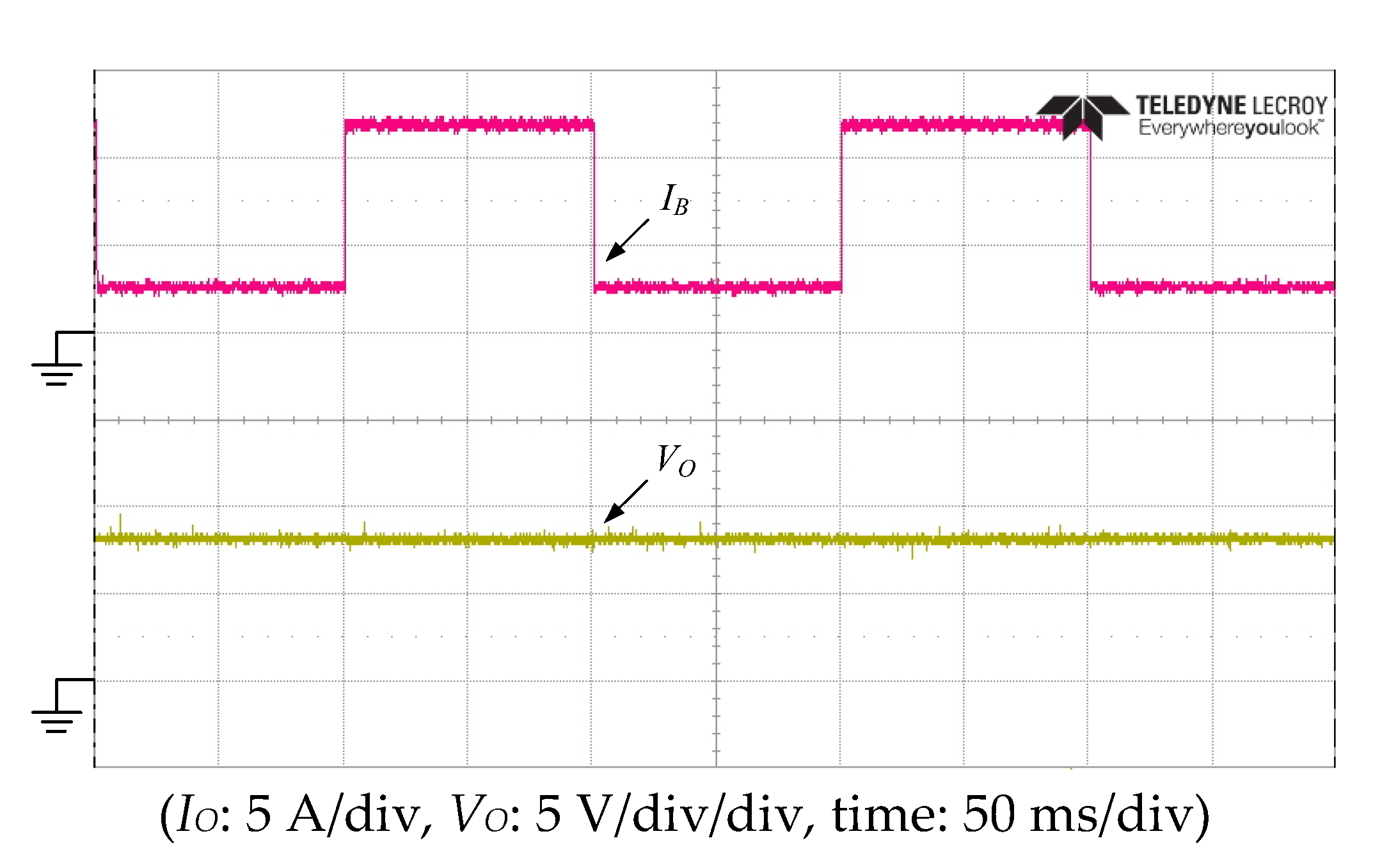
When the proposed hybrid converter uses solar power as its input source, it has to possess a good dynamic response. In order to verify the dynamic response of the proposed hybrid converter, Figure 17 illustrates measured battery voltage VB and current IB waveforms under step-load changes between IB = 0 A and IB(max) = 12 A. In Figure 17, battery voltage VB varies within ±1%, from which it can be observed that the proposed hybrid converter operated in the solar power condition has a good dynamic response. Figure 18 shows measured solar power voltage VPV, current IPV and power PPV waveforms under the maximum solar power PPV(max) = 50 W. In Figure 18, when solar power PPV varies from 0 W to 50 W, the MPPT time interval is about 330 ms. That is, the proposed hybrid converter can achieve MPPT features. Figure 19 expresses the conversion efficiency curve of the proposed hybrid converter operated in the solar power condition from light load to heavy load. In Figure 19, the maximum conversion efficiency is 95% under 80% of the full-load condition. When the proposed hybrid converter is operated under 100% of full-load condition, its conversion efficiency is about 91%. According to power loss analysis, driving circuit and stray losses are about 21.7% of total power loss. Losses of switches are approximated to 42.7%, while losses of transformer Tr are approximately 35.6%. As mentioned above, the proposed hybrid converter can be operated in the solar power condition to achieve battery charging.
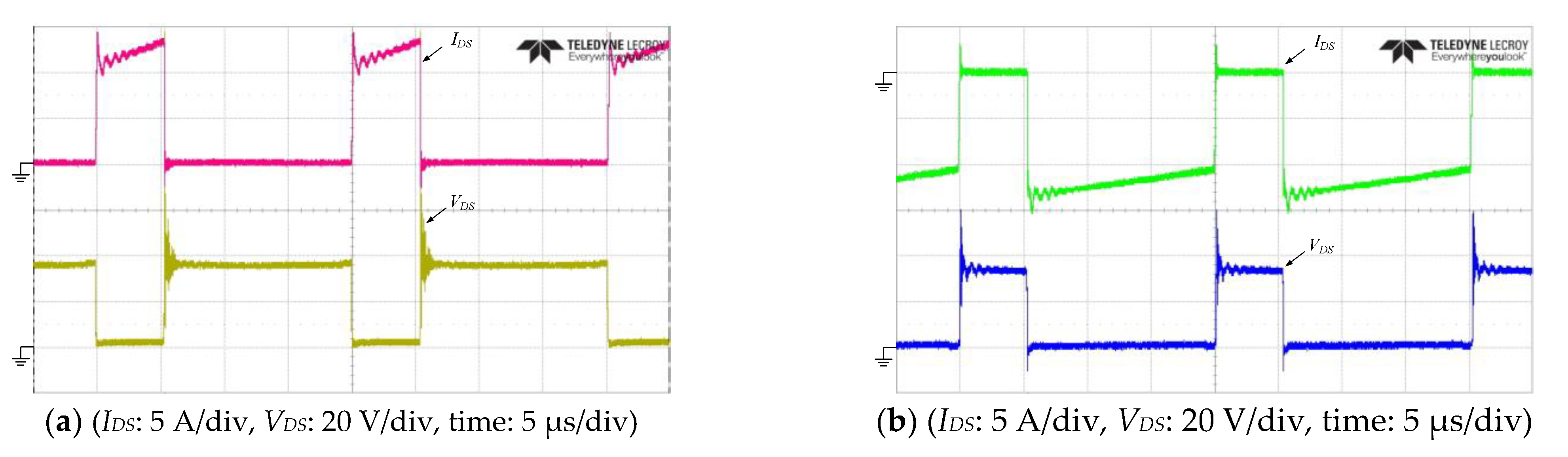
When the proposed hybrid converter adopts the utility line as its input source, some experimental results are measured to verify its feasibility. Figure 20 and Figure 21 illustrate measured switch voltage VDS and current IDS of the proposed hybrid converter operated in the utility line condition. Figure 20 shows those waveforms under 45% of the full-load condition, while Figure 21 expresses those waveforms under 100% of the full-load condition. From Figure 20 and Figure 21, it can be observed that switches M1 and M2 are operated with ZVS at the turn-on transition. Figure 22 depicts measured battery voltage VB and current IB waveforms of the proposed one operated in the utility line condition under different charging currents. Figure 22a shows those waveforms under IB = 3 A, while Figure 22b illustrates those waveforms under IB = 6 A. In Figure 22, the charging current IB can be successfully changed. Measured battery voltage VB and current IB waveforms of the proposed one operated in the utility line condition under step-load changes from IB = 2.4 A to IB(max) = 12 A are illustrated in Figure 23. Its battery voltage, VB, can be kept within ±1% to verify a good dynamic response. Figure 24 draws the conversion efficiency curve of the proposed one operated in the utility line condition from light loads to heavy loads. The maximum conversion efficiency is about 93% under 70% of the full-load condition. When the proposed hybrid converter is operated under 100% of the full-load condition, its conversion efficiency is about 89%. According to power loss analysis, driving circuit and stray losses is about 4.3% of total power loss. Losses of switches are approximated to 88.1%, while losses of transformer Tr are approximately 7.6%. As previously experiment results, the proposed hybrid converter can be operated in the utility line condition to achieve battery charging.
7. Conclusions
This paper proposes a hybrid converter using multiple sources to charge lithium battery. The proposed hybrid converter consists of a buck converter and flyback converter to achieve battery charging under different input sources. Compared with its counterparts, the proposed hybrid converter can reduce component counts when the proposed one adds an extra switch with low speed and low cost. In this paper, circuit simplification of the proposed one is described for reducing component counts. In addition, operational principles, steady-state analysis and design of the proposed converter have been described in detail. From experiment results, it can be observed that the proposed hybrid converter can be operated in different input sources, such as the utility line and solar power sources. When the proposed hybrid converter is operated in the solar power condition, it can implement different charging currents and achieve MPPT operations. Moreover, its maximum conversion efficiency is about 95% under 80% of the full-load condition and its conversion efficiency of the full-load condition is about 91%. When the proposed one is operated in the utility line condition, switches M1 and M2 can be operated with ZVS at the turn-on transition. Its maximum conversion efficiency is about 93% under 70% of the full-load condition, and its conversion efficiency of the full-load condition is about 89%. An experimental prototype has been implemented for lithium battery charger of 8.4 V/12 A. It can verify the feasibility of the proposed hybrid converter for lithium battery charging under different input sources.
Author Contributions
Conceptualization, S.-Y.T.; Formal analysis, J.-H.F.; Validation, H.-K.H. All authors have read and agreed to the published version of the manuscript.
Funding
This research was funded by MOST in Taiwan, grant number MOST 110-2221-E-182-040.
Conflicts of Interest
The authors declare no conflict of interest.
References
- Veeramallu, V.K.S.; Porpandiselvi, S.; Narasimharaju, B.L. A Nonisolated Wide Input Series Resonant Converter for Automotive LED Lighting System. IEEE Trans. Power Electron. 2021, 36, 5686–5689. [Google Scholar] [CrossRef]
- Malschitzky, A.; Agostini, E.; Nascimento, C.B. Integrated Bridgeless-Boost Nonresonant Half-Bridge Converter Employing Hybrid Modulation Strategy for LED Driver Applications. IEEE Trans. Ind. Electron. 2021, 68, 8049–8060. [Google Scholar] [CrossRef]
- Cao, Y.; Li, K.; Lu, M. Balancing Method Based on Flyback Converter for Series-Connected Cells. IEEE Access 2021, 9, 52393–52403. [Google Scholar] [CrossRef]
- Singh, B.; Kushwaha, R. Power Factor Preregulation in Interleaved Luo Converter-Fed Electric Vehicle Battery Charger. IEEE Trans. Ind. Appl. 2019, 57, 2870–2872. [Google Scholar] [CrossRef]
- Abdelmessih, G.Z.; Alonso, J.M.; Tsai, W.T. Analysis and Experimentation on a New High Power Factor Off-Line LED Driver Based on Interleaved Integrated Buck Flyback Converter. IEEE Trans. Ind. Appl. 2019, 55, 4359–4459. [Google Scholar] [CrossRef]
- Abdelmessih, G.Z.; Alonso, J.M. Loss analysis for efficiency improvement of the integrated buck-flyback converter for LED driving applications. IEEE Ind. Appl. Soc. Annu. Meet. 2018, 54, 6543–6553. [Google Scholar]
- Nazi, H.; Babaei, E. A Modularized Bidirectional Charge Equalizer for Series Connected Cell Strings. IEEE Trans. Ind. Electron. 2021, 68, 6739–6749. [Google Scholar] [CrossRef]
- Ahmadi, F.; Adib, E.; Azari, M. Soft Switching Bidirectional Converter for Reflex Charger with Minimum Switches. IEEE Trans. Ind. Electron. 2020, 67, 8355–8362. [Google Scholar] [CrossRef]
- Su, M.; Wu, S.; Dan, H.; Xu, J.; Sun, Y.; Wang, H.; Liu, Y.; Xiong, W.; Liang, X. A Natural Bidirectional Isolated Single-Phase AC/DC Converter with Wide Output Voltage Range for Aging Test Application in Electric Vehicle. IEEE J. Emerg. Sel. Top. Power Electronics. 2021, 9, 3489–3500. [Google Scholar] [CrossRef]
- Hunter, B.L.; Matthews, W.E. A 100-V Battery Charger Voltage Extender IC With 97% Efficiency at 4-A and ±0.5% Voltage Accuracy. IEEE Trans. Circuits Syst. 2020, 67, 2492–2502. [Google Scholar] [CrossRef]
- Wang, C.; Sun, D.; Zhang, X.; Hu, J.; Gu, W.; Gui, S. A Constant Current Digital Control Method for Primary-Side Regulation Active-Clamp Flyback Converter. IEEE Trans. Power Electron. 2019, 36, 3989–4000. [Google Scholar]
- Xu, S.; Qian, Q.; Tao, T.; Lu, S.; Sun, W. Small Signal Modeling and Control Loop Design of Critical Conduction Mode Active Clamp Flyback Converter. IEEE Trans. Power Electron. 2019, 36, 7250–7263. [Google Scholar] [CrossRef]
- Jo, S.W.; Seok, H.; Kim, M. Dual-Mode Resonant Flyback Single Power-Conversion Inverter. IEEE Trans. Ind. Electron. 2021, 68, 5776–5787. [Google Scholar] [CrossRef]
- Jeong, M.G.; Kim, S.H.; Yoo, C. Switching Battery Charger Integrated Circuit for Mobile Devices in a 130-nm BCDMOS Process. IEEE Trans. Power Electron. 2016, 31, 7943–7952. [Google Scholar] [CrossRef]
- Lee, W.S.; Kim, J.H.; Lee, J.Y.; Lee, I.O. Design of an Isolated DC/DC Topology with High Efficiency of over 97% for EV Fast Chargers. IEEE Trans. Veh. Technol. 2019, 68, 11725–11737. [Google Scholar] [CrossRef]
- Aamir, M.; Mekhilef, S. An Online Transformer less Uninterruptible Power Supply (UPS) System with a Smaller Battery Bank for Low-Power Applications. IEEE Trans. Power Electron. 2016, 32, 233–247. [Google Scholar] [CrossRef]
- Mukhtar, N.M.; Lu, D.D.C. A Bidirectional Two-Switch Flyback Converter with Cross-Coupled LCD Snubbers for Minimizing Circulating Current. IEEE Trans. Ind. Electron. 2019, 66, 5948–5957. [Google Scholar] [CrossRef]
- Cheng, H.L.; Chang, Y.N.; Yen, H.C.; Hua, C.C.; Su, S.P. An Interleaved Flyback-Typed LED Driver with ZVS and Energy Recovery of Leakage Inductance. IEEE Trans. Power Electron. 2019, 34, 4497–4508. [Google Scholar] [CrossRef]
- Zhang, F.; Xie, Y.; Hu, Y.; Chen, G.; Wang, X. A Hybrid Boost–Flyback Flyback Microinverter for Photovoltaic Applications. IEEE Trans. Ind. Electron. 2020, 67, 308–318. [Google Scholar] [CrossRef]
- Tseng, S.Y.; Hauang, P.J.; Wu, D.H. Power Factor Corrector with Bridgeless Flyback Converter for DC Loads Applications. Energies 2018, 11, 3096. [Google Scholar] [CrossRef] [Green Version]
- Falcones, S.; Ayyanar, R.; Mao, X. A DC–DC Multiport-Converter-Based Solid-State Transformer Integrating Distributed Generation and Storage. IEEE Trans. Power Electron. 2013, 28, 2192–2203. [Google Scholar] [CrossRef]
- Akar, F.; Tavlasoglu, Y.; Ugur, E.; Vural, B.; Aksoy, I. A Bidirectional Nonisolated Multi-Input DC–DC Converter for Hybrid Energy Storage Systems in Electric Vehicles. IEEE Trans. Veh. Technol. 2016, 65, 7944–7955. [Google Scholar] [CrossRef]
- Kumar, M.; Babu, Y.N.; Pullaguram, D.; Mishra, S. A high voltage gain non-isolated modified three-port DC/DC converter based on integrated Boost-Cuk topology. In Proceedings of the 2017 IEEE PES Asia-Pacific Power and Energy Engineering Conference (APPEEC)s, Bangalore, India, 8–10 November 2017. [Google Scholar]
- Wu, H.; Xing, Y.; Xia, Y.; Sun, K. A family of non-isolated three-port converters for stand-alone renewable power system. In Proceedings of the IECON 2011–37th Annual Conference of the IEEE Industrial Electronics Society, Melbourne, Australia, 7–10 November 2011. [Google Scholar]
- Wu, H.; Zhang, J.; Xing, Y. A Family of Multiport Buck–Boost Converters Based on DC-Link-Inductors (DLIs). IEEE Trans. Power Electron. 2015, 30, 735–746. [Google Scholar] [CrossRef]
- Wu, Y.E.; Chiu, P.N. A High-Efficiency Isolated-Type Three-Port Bidirectional DC/DC Converter for Photovoltaic Systems. Energies 2017, 10, 434. [Google Scholar] [CrossRef] [Green Version]
- Manoharan, P.; Subramaniam, U.; Babu, T.S.; Padmanaban, S.; Bo, J.; Nielsen, H.; Mitolo, M.; Ravichandran, S. Improved Perturb and Observation Maximum Power Point Tracking Technique for Solar Photovoltaic Power Generation Systems. IEEE Syst. J. 2021, 15, 3024–3035. [Google Scholar] [CrossRef]
Figure 1.
Schematic diagram of flyback converter for battery charging system.

Figure 2.
Schematic diagram of buck converter for battery charging system.

Figure 3.
Schematic diagram of the conventional flyback/buck hybrid converter with utility line and PV arrays sources for lithium battery charger system.
Figure 3.
Schematic diagram of the conventional flyback/buck hybrid converter with utility line and PV arrays sources for lithium battery charger system.

Figure 4.
Schematic diagram of the proposed hybrid converter.

Figure 5.
Circuit derivation of the proposed hybrid converter with utility line and PV arrays sources for lithium battery charger system: (a).step 1, (b) step 2, (c) step 3, (d) step 4, (e) step 5 and (f) step6.
Figure 5.
Circuit derivation of the proposed hybrid converter with utility line and PV arrays sources for lithium battery charger system: (a).step 1, (b) step 2, (c) step 3, (d) step 4, (e) step 5 and (f) step6.


Figure 6.
Equivalent circuit of the proposed hybrid converter in (a) buck converter mode for PV array source and (b) flyback converter mode for utility line source.
Figure 6.
Equivalent circuit of the proposed hybrid converter in (a) buck converter mode for PV array source and (b) flyback converter mode for utility line source.

Figure 7.
Equivalent circuit of each operational mode of the proposed hybrid converter operated in PV arrays source condition over a complete switching cycle. (a) Mode1 (t0 ≤ t ≤ t1), (b) Mode2 (t1 ≤ t ≤ t2), (c) Mode3 (t2 ≤ t ≤ t3), (d) Mode4 (t3 ≤ t ≤ t4) and (e) Mode5 (t4 ≤ t ≤ t5).
Figure 7.
Equivalent circuit of each operational mode of the proposed hybrid converter operated in PV arrays source condition over a complete switching cycle. (a) Mode1 (t0 ≤ t ≤ t1), (b) Mode2 (t1 ≤ t ≤ t2), (c) Mode3 (t2 ≤ t ≤ t3), (d) Mode4 (t3 ≤ t ≤ t4) and (e) Mode5 (t4 ≤ t ≤ t5).


Figure 8.
Conceptual waveforms of each operational mode of the proposed hybrid converter operated in the PV arrays source condition over a complete switching cycle.
Figure 8.
Conceptual waveforms of each operational mode of the proposed hybrid converter operated in the PV arrays source condition over a complete switching cycle.

Figure 9.
Equivalent circuit of each operational mode of the proposed hybrid converter operated in the utility line source condition over a complete switching cycle. (a) Mode1 (t0 ≤ t ≤ t1), (b) Mode2 (t1 ≤ t ≤ t2), (c) Mode3 (t2 ≤ t ≤ t3), (d) Mode4 (t3 ≤ t ≤ t4), (e) Mode5 (t4 ≤ t ≤ t5), (f) Mode6 (t5 ≤ t ≤ t6), (g) Mode7 (t6 ≤ t ≤ t7), (h) Mode8 (t7 ≤ t ≤ t8), (i) Mode9 (t8 ≤ t ≤ t9) and (j) Mode10 (t9 ≤ t ≤ t10).


Figure 10.
Conceptual waveforms of each operational mode of the proposed hybrid converter operated in the utility line source condition over a complete switching cycle.
Figure 10.
Conceptual waveforms of each operational mode of the proposed hybrid converter operated in the utility line source condition over a complete switching cycle.

Figure 11.
Ideal waveforms of inductor current ILm and charging current IB1 of the proposed flyback converter operated in the boundary of CCM and DCM.
Figure 11.
Ideal waveforms of inductor current ILm and charging current IB1 of the proposed flyback converter operated in the boundary of CCM and DCM.

Figure 12.
Ideal waveforms of inductor current IDS2, IDS3 and IB2 of the proposed buck converter operated in the boundary of CCM and DCM.
Figure 12.
Ideal waveforms of inductor current IDS2, IDS3 and IB2 of the proposed buck converter operated in the boundary of CCM and DCM.

Figure 13.
Block diagram of controller for the proposed hybrid converter.

Figure 14.
Measured waveforms of switch voltage VDS and current IDS under 25% of the full-load condition when VPV = 36 V: (a) switch M2 and (b) switch M3.
Figure 14.
Measured waveforms of switch voltage VDS and current IDS under 25% of the full-load condition when VPV = 36 V: (a) switch M2 and (b) switch M3.

Figure 15.
Measured waveforms of switch voltage VDS and current IDS under 100% of the full-load condition when VPV = 36 V: (a) switch M2 and (b) switch M3.
Figure 15.
Measured waveforms of switch voltage VDS and current IDS under 100% of the full-load condition when VPV = 36 V: (a) switch M2 and (b) switch M3.

Figure 16.
Measured battery voltage VB and current IB waveforms: (a) under IB = 3 A and (b) under IB = 6 A when VPV = 36 V.
Figure 16.
Measured battery voltage VB and current IB waveforms: (a) under IB = 3 A and (b) under IB = 6 A when VPV = 36 V.

Figure 17.
Measured battery voltage VB and current IB waveforms under step-load changes between IB = 0A and IB(max) = 12A when battery voltage VB = 8V.
Figure 17.
Measured battery voltage VB and current IB waveforms under step-load changes between IB = 0A and IB(max) = 12A when battery voltage VB = 8V.

Figure 18.
Measured solar voltage VPV, current IPV and power PPV waveforms under the maximum solar power PPV(max) = 50W.
Figure 18.
Measured solar voltage VPV, current IPV and power PPV waveforms under the maximum solar power PPV(max) = 50W.

Figure 19.
Conversion efficiency curve of the proposed hybrid converter operated in the solar power condition from light loads to heavy loads.
Figure 19.
Conversion efficiency curve of the proposed hybrid converter operated in the solar power condition from light loads to heavy loads.

Figure 20.
Measured switch voltage VDS and current IDS of the proposed hybrid converter operated in the utility line condition under 45% of the full-load condition: (a) switch M1 and (b) switch M2.
Figure 20.
Measured switch voltage VDS and current IDS of the proposed hybrid converter operated in the utility line condition under 45% of the full-load condition: (a) switch M1 and (b) switch M2.

Figure 21.
Measured switch voltage VDS and current IDS of the proposed hybrid converter operated in the utility line condition under 100% of the full-load condition: (a) switch M1 and (b) switch M2.
Figure 21.
Measured switch voltage VDS and current IDS of the proposed hybrid converter operated in the utility line condition under 100% of the full-load condition: (a) switch M1 and (b) switch M2.

Figure 22.
Measured battery voltage VB and current IB waveforms of the proposed hybrid converter operated in the utility line condition (a) under IB = 3 A and (b) under IB = 6 A.
Figure 22.
Measured battery voltage VB and current IB waveforms of the proposed hybrid converter operated in the utility line condition (a) under IB = 3 A and (b) under IB = 6 A.

Figure 23.
Measured battery voltage VB and current IB waveforms of the proposed hybrid converter operated in the utility line condition under step-load changes from IB = 2.4A to IB(max) = 12A.
Figure 23.
Measured battery voltage VB and current IB waveforms of the proposed hybrid converter operated in the utility line condition under step-load changes from IB = 2.4A to IB(max) = 12A.

Figure 24.
Conversion efficiency curve of the proposed hybrid converter operated in the utility line condition from light loads to heavy loads.
Figure 24.
Conversion efficiency curve of the proposed hybrid converter operated in the utility line condition from light loads to heavy loads.


Table 1.
Comparison of component counts with the proposed hybrid converter and its counterparts.
| Three-Port Converter | Input Ports | Output Ports | Inductors | Transformers | Switches | Diodes | Capacitors | Extra Switches |
|---|---|---|---|---|---|---|---|---|
| M. Kumar, et al. [23] | 2 | 1 | 2 | 0 | 3 | 3 | 3 | 0 |
| H. Wu, et al. [24] | 2 | 1 | 2 | 0 | 3 | 3 | 1 | 0 |
| H. Wu, et al. [25] | 2 | 1 | 3 | 0 | 3 | 3 | 1 | 0 |
| Y-E. Wu, et al. [26] | 2 | 1 | 1 | 1 | 4 | 2 | 3 | 0 |
| The proposed Hybrid converter (Figure 4) | 2 | 1 | 0 | 1 | 3 | 0 | 1 | 1 |
Table 2.
Definitions of key parameters in Figure 13 for the controller of the proposed hybrid converter.
Table 2.
Definitions of key parameters in Figure 13 for the controller of the proposed hybrid converter.
| Symbol | Definition | Symbol | Definition |
|---|---|---|---|
| VPV | output voltage of solar power | SDI | protection signal of IB ≥ IBP |
| VPV(min) | minimum output voltage of solar power | SDV | protection signal of VB ≥ VBP |
| VDC | equivalent dc voltage of utility line | SD | protection signal of battery |
| VDC(min) | minimum equivalent dc voltage of utility line | SPV | detector signal of VPV ≥ VPV(min) |
| VB | battery voltage | SDC | detector signal of VDC ≥ VDC(min) |
| VB(max) | maximum battery voltage | PSP | selector signal of solar power |
| VBP | voltage protection of battery | PUL | selector signal of utility line |
| IB | Battery current | M11 | gate signal of switch M1 under utility line source |
| IB(max) | maximum charging current of Battery | M12 | gate signal of switch M2 under utility line source |
| IBP | current protection of battery | M13 | gate signal of switch M3 under utility line source |
| PPV(max) | maximum output power of solar power at present | M21 | gate signal of switch M1 under solar power source |
| IBcom1 | current command value under PPV(max) | M22 | gate signal of switch M2 under solar power source |
| IBcom | current command value with CC charging method | M23 | gate signal of switch M3 under solar power source |
| Scc | selecting signal of CC command | M1 | gate signal of switch M1 |
| Scm | selecting signal of CC/CV command | M2 | gate signal of switch M2 |
| Vref | command signal of PWM generator | M3 | gate signal of switch M3 |
| Vf | feedback signal of PWM generator | S1 | gate signal of switch S1 |
| SPWM | PWM signal of main switch generator |
Table 3.
Operational condition of the proposed hybrid converter for the controller shown.
| Controlling Unit | Selection/Judgement Condition | Operational Condition | |||||
|---|---|---|---|---|---|---|---|
| Variable | State | ||||||
| Power source selection unit | solar power detector | SPV | High | VPV ≥ VPV(min) | |||
| Low | VPV < VPV(min) | ||||||
| utility line detector | SDC | High | High | VDC ≥ VDC(min) | |||
| Low | Low | VDC < VDC(min) | |||||
| power source selector | PSP | High | under the solar power condition | ||||
| Low | Shutdown solar power | ||||||
| PSP | High | under the solar utility line condition | |||||
| Low | Low | Shutdown utility line | |||||
| CC command selection unit | solar power command | IBcom1 | |||||
| Charging current selector | Scc | High | IBcom1 ≥ IB(max) | ||||
| Low | IBcom1 < IB(max) | ||||||
| CC command selector | IBcom | Scc = High | IBcom = IB(max) | ||||
| Scc = Low | IBcom = IBcom1 | ||||||
| CC/CV command unit | Charging mode judgement | Scm | High | VB ≥ VB(max) | |||
| Low | VB < VB(max) | ||||||
| CC/CV command selector | Vref | Scm = High | Vref = VB(max) under CV operation | ||||
| Scm = Low | Vref = IBcom under CC operation | ||||||
| PWM generator unit | Feedback selector | Vf | Scm = High | Vf = VB under CV operation | |||
| Scm = Low | Vf = IB under CC operation | ||||||
| PWM generator | SPWM | Error value by Vref and Vf | |||||
| Gate driver | M11 | M11 = SPWM | |||||
| under utility | M12 | M12 | |||||
| line source | M13 | M13 | |||||
| Gate driver | M21 | turn-off | |||||
| under solar | M22 | M22 = SPWM | |||||
| power source | M23 | M23 | |||||
| PWM signal selector | M1 | M1 = PUL M11 + PSP M21 | |||||
| M2 | M2 = PUL M12 + PSP M22 | ||||||
| M3 | M3 = PUL M13 + PSP M23 | ||||||
| S1 | PSP = High | S1 = Low | |||||
| PUL = High | S1 = High | ||||||
| SD | High | shutdown the proposed hybrid converter | |||||
| Low | normal operation | ||||||
| Battery protection unit | IB protection | SDI | High | IB ≥ IBP | |||
| Low | IB < IBP | ||||||
| VB protection | SDV | High | VB ≥ VBP | ||||
| Low | VB < VBP | ||||||
| battery protection | SD | SD = SDI + SDV | |||||
Table 4.
Specifications of solar panel.
| Parameters | Single Module Value | Series Module Value |
|---|---|---|
| Maximum Power PPV(max) | 50 W | 100 W |
| Open circuit voltage VDC | 22.5 V | 45 V |
| Maximum Power voltage VPV(max) | 17.96 V | 36 V |
| Maximum Power current IPV(max) | 2.78 A | 2.78 A |
| Short circuit current ISC | 3.1 A | 3.1 A |
Table 5.
Specifications of lithium battery.
| Parameters | Single Battery Cell | Battery Pack: 2 Series *8 Parallel | ||
|---|---|---|---|---|
| Rated Value | Practical Value | Rated Value | Practical Value | |
| Rated capacity | 3.2 Ah | 3.2 Ah | 25.6 Ah | 25.6 Ah |
| Nominal voltage VB(NV) | 3.6 V | 3.6 V | 7.2 V | 7.2 V |
| Maximum voltage VB(max) | 4.2 V | 4.2 V | 8.4 V | 8.4 V |
| Protection voltage VBP | 4.3 V | 8.6 V | ||
| Maximum charging current IB(max) | 1.625 A | 1.5 A | 6.5 A | 6 A |
| Protection current IBP | 1.6 A | 6.4 A | ||
| Maximum discharging current IBD(max) | 6.4 A | 25.6 A | ||
| Minimum discharging voltage VB(min) | 2.5 V | 2.5 V | 5 V | 5 V |
Table 6.
Key components of the proposed hybrid converter.
| Symbol | Material Type | Power Rating/Value |
|---|---|---|
| Switch M1 | STF13NM60N | 650 V/11 A |
| Switch M2 | STO36N60M6 | 600 V/30 A |
| Switch M3 | AOW2918 | 100/90 A |
| Switch S1 | STF13NM60N | 650 V/11 A |
| Capacitor Cc | Mpp Capacitor | 0.4 F/400 V |
| Transformer Tr | EE-33 CORE | Lm = 3.6 mH, LK = 40µH, N = 9 |
Publisher’s Note: MDPI stays neutral with regard to jurisdictional claims in published maps and institutional affiliations. |
© 2022 by the authors. Licensee MDPI, Basel, Switzerland. This article is an open access article distributed under the terms and conditions of the Creative Commons Attribution (CC BY) license (https://creativecommons.org/licenses/by/4.0/).
Share and Cite
MDPI and ACS Style
Tseng, S.-Y.; Fan, J.-H.; Huang, H.-K. Hybrid Converter with Multiple Sources for Lithium Battery Charger Applications. Electronics 2022, 11, 616. https://doi.org/10.3390/electronics11040616
AMA Style
Tseng S-Y, Fan J-H, Huang H-K. Hybrid Converter with Multiple Sources for Lithium Battery Charger Applications. Electronics. 2022; 11(4):616. https://doi.org/10.3390/electronics11040616
Chicago/Turabian StyleTseng, Sheng-Yu, Jun-Hao Fan, and Hong-Kai Huang. 2022. "Hybrid Converter with Multiple Sources for Lithium Battery Charger Applications" Electronics 11, no. 4: 616. https://doi.org/10.3390/electronics11040616
Note that from the first issue of 2016, this journal uses article numbers instead of page numbers. See further details here.