
A Low-Power, Fast-Transient Output-Capacitorless LDO with Transient Enhancement Unit and Current Booster
by
Yongchao Jiang
1,2, 
Lixin Wang
1,2,*,
Shixin Wang
1,2,
Mengyao Cui
1,
Zhuoxuan Zheng
1 and
Yuanzhe Li
1,2 1
Institute of Microelectronics of the Chinese Academy of Sciences, Beijing 100029, China
2
University of Chinese Academy of Sciences, Beijing 100049, China
*
Author to whom correspondence should be addressed.
Electronics 2022, 11(5), 701; https://doi.org/10.3390/electronics11050701
Submission received: 31 December 2021
/
Revised: 4 February 2022
/
Accepted: 23 February 2022
/
Published: 24 February 2022
(This article belongs to the Section Power Electronics)
Abstract
:With the wide application of advanced portable devices, output-capacitorless low dropout regulators (OCL-LDO) are receiving increasing attention. This paper presents a low quiescent current OCL-LDO with fast transient response. A transient enhancement unit (TEU) is proposed as the output voltage-spike detection circuit. It enhances the transient response by improving the slew-rate at the gate of the power transistor. In addition, a current booster (CB), which consists of a current subtractor and a non-linear current mirror, is designed to improve the slew-rate further. The current subtractor increases the transconductances of the differential-input transistors to obtain a large slewing current, while the non-linear current mirror further boosts the current with no extra quiescent current consumption. The simulated results show that the proposed OCL-LDO is capable of supplying 100 mA load current while consuming 10.3 μA quiescent current. It regulates the output at 1 V from a supply voltage ranging from 1.2 to 1.8 V. When the load current is stepped from 1 mA to 100 mA in 100 ns, the OCL-LDO has attained a settling time of 190 ns, and the output voltage undershoot and overshoot are controlled under 110 mV.
1. Introduction
Low dropout regulator (LDO) is an integral part of electronic systems. An external capacitor is widely used in the traditional LDO to stabilize the feedback loop and improve the transient response. Output-capacitorless low-dropout regulators (OCL-LDOs) have received much attention recently, due to the increasing demand for system-on-chip (SoC) [1,2,3,4]. Removal of the bulky off-chip capacitor saves the printed-circuit-board (PCB) space [5]. However, the transient response performance of the OCL-LDO may be degraded without the microfarad output capacitor.
Typically, transient variations of OCL-LDOs depend on the slew-rate conditions at the gate of the power transistor and the closed-loop bandwidth [6,7,8,9]. Some compensation techniques, for example, DFC [10] and Q-reduction [11] can extend the loop bandwidth with a small on-chip capacitor, while they are both limited by the minimum load current. A tri-loop OCL-LDO based on the FVF (flipped voltage follower) structure in [12] is capable of achieving ultra-fast transient response due to the wide bandwidth, but the loop gain is insufficient. Thus, the fast transient OCL-LDO may suffer from the poor regulation. Usually, a wide unity-gain bandwidth means there will be a large quiescent current [13,14]. The OCL-LDO in [15] achieved both the wide bandwidth and the high DC gain by utilizing multiple feedback loops, at the expense of on-chip capacitance and quiescent current [16]. A fast-transient OCL-LDO using active-feedback and current-reuse feedforward compensation was presented in [17], but it also consumed a high quiescent current. Current efficiency, which refers to the ratio of load to input current, determines operational life in the world of portable electronics [18,19]. The ultralow-power OCL-LDO in portable devices can prolong the battery life at the sacrifice of transient performance [20]. The capability to drive the power transistor can be enhanced by utilizing a high slew-rate class-AB amplifier, which will result in an improved transient performance [21]. The slew-rate enhanced circuit can also improve the slew-rate at the gate of the power transistor during the transient response; however, it may be detrimental to the loop stability [22]. Therefore, the tradeoffs between stability issues, transient performance, and quiescent current consumption are still challenges for designers.
This paper presents a low-power, fast-transient response OCL-LDO with a high slew-rate class-AB error amplifier. Section 2 introduces the basic characteristics of the proposed TEU and CB. The loop stability and transistor-level design considerations are also discussed. In Section 3, the post-simulation results and discussion are presented. Finally, the conclusion is drawn.
2. Proposed LDO Topology
Figure 1 shows the conceptual schematic of the proposed fast transient OCL-LDO. The OCL-LDO consists of a high slew-rate error amplifier and a pass element Mpass. The capacitor CP represents the gate parasitic capacitor of the power transistor. Gm cells, the proposed transient enhancement unit (TEU) and the current booster (CB) construct the high slew-rate error amplifier. The TEU and the CB consume a low quiescent current at steady state. The TEU senses the output variation and transfers it to a transient bias current of Gm cells during the load current transitions. Consequently, Iin+ decreases and Iin− increases rapidly. Then, Iin− will be boosted several times to quickly discharge Cp through the current booster. Thus, a fast transient response can be achieved. The circuit implements and considerations will be discussed in detail in the following subsections.
2.1. Transient Enhancement Unit (TEU)
The Gm cell presented in [24] is shown in the red dashed box in Figure 2a. IB+ and IB− are the constant tail current source and the four transistors have the same sizes (W/L). VREF and VOUT are the input voltage of the Gm cell. The output currents Iout− and Iout+ are not limited by the tail current source and have a quadratic dependence on (VOUT−VREF), where Iout− can be expressed as:
where is the mobility of carriers, is the gate-oxide capacitance per unit area and IB, which is the constant current source, is equal to IB+ and IB−. However, the slew-rate is still limited by the transconductance of the differential-input transistors. A large tail current IB− can be used to boost the transconductance of the differential-input transistors, but the quiescent current is also increased.
The proposed TEU acts as an output voltage detector [25,26], as shown in the pink box in Figure 2a. It consumes no additional quiescent current and provides a large slewing current during the transient response. Figure 2b shows the operational principle comparison of the two structures in Figure 2a. When the load current steps down, Cf senses the output positive voltage spike (VOUT-VREF) so that the gate voltage of M2A goes down and the gate voltage of M2B goes up. Then, IB− rises while VREF is a constant, which will lead to the voltage drop of VL. As the source voltage of ML2 (VOUT) increases and the gate voltage of ML2 (VL) decreases, the voltage difference between its source and gate is much higher than it is in the red box in Figure 2a, resulting in a higher Iout−. At the same time, the increase of VOUT contributes to a much more significant increase in VH than it is in the red box in Figure 2a, due to the decrease of IB+. Thus, Iout+ in the green dashed box is much lower than it is in the red dashed box in Figure 2a. The bias current of MfA and MfB is IB. M2A and M2B are both biased in the subthreshold region in this work, and the total transient current in ML1 can be expressed as:
where k is a constant, VDS2 is the drain-source voltage of M2B. IS0, n, and λsub are the process-related parameters.
It can be seen that IB- is equal to IB at steady state, i.e., VOUT-VREF = 0. When VOUT varies during the transient response, IB− will change quickly. As a result, the slewing current IOUT− is boosted and can be expressed as:
Based on Equations (1)–(3), the proposed TEU achieves a higher Iout− or Iout− during the output current transitions, while no extra quiescent current is generated, as shown in Figure 3. Assuming MH1, MH2, ML1, and ML2 have the same sizes, and VOUT = VREF when operating at a steady state, the output current of Gm cells is equal to IB, with or without TEU structure. The transient output current in the proposed TEU structure is higher than that in the classical structure, with the same output voltage variation (VOUT-VREF).
2.2. Current Booster
Current mirrors are widely used in Class-AB OTA topologies [27]. Figure 4a illustrates the classical current mirror structure. M1 and M2 are both in the saturation region, and the ratio of the output current Iout1 to the input current Iin1 is equal to the scale factor A.
The nonlinear current mirror structure is applied to maintain a low quiescent current and boost the output current when Iin increases. Figure 4b shows that the nonlinear current mirror is implemented by adding transistor M3. The bias voltage VB is set to ensure that the transistor M1 operates near the ohmic region, i.e., VDS is slightly higher than VDS,sat. Vx will decrease when Iin increases due to the fixed bias voltage VB. Hence, the drain-source voltage of M1 is lower than its VDS,sat, which will drive it to the ohmic region. The current boosting is realized as long as M2 is in the saturation region. Because the VDS is low, the drain-source voltage of M1 can be approximately expressed as:
where un and Cox are the process-related parameters and VTHN is the threshold voltage of M3. VDS1 decreases as Iin rising. The output current Iout2 can be expressed as:
where A is the scale factor. Iout2 is larger than the output current Iout1 of the traditional current mirror structure in Figure 4a.
Figure 5 shows the simulated dc responses of the traditional current mirror and the nonlinear current mirror at A = 2. If the bias voltage VB is biased properly to make M1 near the ohmic region, the output current will boost as Iin increases, even with a small scale factor.
2.3. Circuit Implementation
The transistor-level schematic of the proposed OCL-LDO is shown in Figure 6. A unity-gain buffer is applied between the voltage reference Vref and the input of the OCL-LDO core, because many voltage references cannot provide the output current. The tail current in the transistor MB9 is set to 200 nA as the buffer does not require a high slew-rate. In this design, the bias current IB is set to 500 nA. A current subtractor [28] is introduced in the current booster to enhance the transconductance of the Gm cells. The size of MH1 (ML1) is twice as large as MH2/MH3 (ML2/ML3) to set the bias point of the current booster. For a differential-input voltage ΔVin, the output current in M11 is 1.5gmΔVin so that the transconductance of the Gm cell is enhanced by 1.5 times. The larger transconductance of the Gm cell contributes to the larger bandwidth and the higher slewing current at the gate of the power transistor, which can improve the performance of the transient response. The transistors M2A and M2B of the TEU, which are operating in the subthreshold region, can optimize the bandwidth, and this will be explained in the following part. The ratios of M12 to M11 and M7 to M6 are set to 4/1 to further improve the slew-rate. A miller capacitor Cc is added between the gate of the power transistor Mpass and Vout to guarantee stability under full load conditions. Thus, this OCL-LDO is stable under full load conditions, and the maximum load capacitor CL is 100 pF. The size of the power transistor Mpass is 8000 um/0.18 um, so that it will operate in the ohmic region under the heavy load condition and in the subthreshold region under the light load condition.
2.4. Stability Analysis
A loop transfer function is derived to evaluate the effect of the proposed transient enhancement unit on the loop stability. Figure 7 shows a small signal block diagram representing the structure in Figure 6. Hence, gmH and gmL are the transconductances of two Gm cells. gmp, gm2, and gmf represent the transconductances of the power transistor Mpass, M2A/M2B, and MfA, respectively. The small-signal impedance at the output of the error amplifier and Vout are denoted as Ro1 and RL (~1/gm), respectively. For the proposed OCL-LDO, it is reasonable to assume Ro1 >> RL. The lumped parasitic capacitances at the gate of the power transistor and the output Vout are modeled as Cg and CL, respectively. Typically, Cg consists of the gate-source parasitic capacitor (Cgs) and the equivalent capacitor because of the miller effect of the gate-drain capacitor (Cgd). Rof and Cof are the small-signal output impedance and the lump parasitic capacitance at the gate of transistor M2A/M2B, respectively. The loop transfer function can be derived and simplified based on the assumption that CL, Cg, and Cf are much larger than Cof.
The loop gain transfer function of the proposed OCL-LDO is:
where TDC is the DC loop gain and N(s) is related to the frequency, they can be expressed as:
The denominator D(s) is:
From Equations (6)–(9), it is clear that the loop transfer function of the OCL-LDO can be simplified to the classical two-stage amplifier with miller compensation by setting Cf to 0. Equations (8) and (9) imply that four zeros and five poles exist in the whole negative feedback loop. No complex pole exists in the system, and locations of poles and zeros are summarized in Table 1.
From Table 1, z4 and p5 will cancel each other so that the loop transfer function can be rewritten as:
The dominant pole p1 and the pole at Vout are established by the effect of Miller capacitor Cc. In addition, z1 is a right-half-plane (RHP) zero caused by the feedforward small-signal current through the miller capacitor. From Table 1, the locations of the additional poles (p3, p4) and zeros (z2, z3) introduced by the proposed transient enhancement unit will not be affected by different load conditions. As p1 and p2 vary with the output current, the loop stability should be studied for different load conditions.
Under light load conditions, gmp is relatively small, and gmpRL is inversely proportional to . The dominant pole is p1, which is at a low frequency. A larger CL indicates that the non-dominant pole p2 is also at a low frequency. As a result, the frequencies of the p1 and p2 are much lower than those of p3, p4, and z3. When the load current is zero and the load capacitor (CL) is maximum, p2 will be close to z2. Thus, the loop acts as a single-pole system. The unity-gain frequency (UGF) can be approximately expressed as:
Under medium to heavy load conditions, gmp becomes quite large due to the large size of Mpass. p2 moves to a much higher frequency than z2. There are two poles (p1, p2) and one zero (z2) existing within the UGF. Thus, the stability can be guaranteed by setting the value of RfCf. Because of the quite small parasitic capacitor Cof, (several fF), z3 and p3 can be assumed to locate at high frequencies and then be ignored. In this case, the UGF is extended due to z2, and it can be expressed as:
Equation (12) indicates that p2 moves to a high frequency as the load current increases, resulting in an increased bandwidth. A higher loop bandwidth means a faster transient response. In other words, the transient enhancement unit acts as a high-pass filter with the dominant pole 1/RfCf and determines the loop stability at high frequencies.
Based on the discussion above, the proposed transient enhancement unit introduces an additional LHP zero and extends the bandwidth. Large Rf and Cf contribute to a fast transient response; however, they may be detrimental to the loop stability. In this design, we set Rf = 200 kΩ and Cf = 1.25 pF to guarantee the loop stability under full load conditions. Figure 8a depicts the simulated loop gain of the proposed OCL-LDO for the load capacitance of 100 pF under different load currents (from 0 mA to 100 mA). It can be seen that the proposed OCL-LDO is stable for all load conditions. Process corner and temperature simulations are also implemented to prove the feasibility of the proposed OCL-LDO. As shown in Figure 8b, for different process corners and temperatures (ff −40 °C, ss 125 °C and tt 25 °C), all phase margins of the proposed OCL-LDO are above 35°, under the full range of load currents. Figure 9 demonstrates the Monte Carlo simulation results of the phase margin of the OCL-LDO with CL = 100 pF when (a) Iload = 10 μA or (b) Iload = 100 mA. Monte Carlo analysis can predict the deviation caused by process and mismatch in the actual circuit. The mean phase margin is 41.5° under light load conditions with a standard deviation of 9.06. Under heavy load conditions, the mean phase margin is 114° with a standard deviation of 5.78. Thus, these prove that the stability of the proposed OCL-LDO can be achieved. The worst stability case occurs when the load current is lowest and the load capacitor is highest.
3. Simulation Results and Discussions
The proposed OCL-LDO is designed and simulated in a 0.18 μm CMOS process. The layout is exhibited in Figure 10, and the whole layout area is approximately 120 × 127 μm. The post-simulation results are shown as follows.
The input voltage range of the proposed OCL-LDO is designed from 1.2 to 1.8 V. The LDO is capable of delivering a current of 100 mA with a dropout voltage of 0.2 V. It is stable when output capacitor values range from 0 to 100 pF. In addition, the OCL-LDO consumes small quiescent current of 10.3 μA and the current efficiency can reach 99.99%. The load regulation is simulated for Vin = 1.2 V, Vin = 1.5 V, and Vin = 1.8 V when VOUT = 1 V with a 100 pF output capacitor. The line regulation is simulated for different load currents (from 1 μA to 100 mA) when VOUT = 1 V. As shown in Figure 11a,b, the load regulation and line regulation are 34 μV/mA and 2.74 mV/V, respectively.
The power supply rejection (PSR) was simulated by adding a sinusoidal signal to a dc input voltage of 1.2 V and observing the output [26]. Figure 12 depicts the PSR of the OCL-LDO under different load currents when VIN = 1.2 V and Vout = 1.0 V.
The load transient response was simulated when the load current is switching from 1 mA to 100 mA, with the rise/fall time of 100 ns, without an output capacitor. As depicted in Figure 13, the maximum output voltage overshoot and undershoot are both less than 110 mV when is 1.0 V. The output voltage variations were about ±10%. The small transient variation under massive load-step is obtained, based on the proposed high-slew rate error amplifier with TEU and CB. Besides, the recovering time is around 190 ns. The large phase margin allows the LDO to achieve the well-behaved settling characteristic.
The line transient response is simulated at Iload = 50 mA with a 100 pF output capacitor. It can assess the impact of the varying input voltage on the output voltage. As shown in Figure 14, when the input voltage changes from 1.2 to 1.8 V with 100 ns rise/fall time, the variation of the output voltage is less than 50 mV.
Table 2 illustrates the performance comparison with some reported OCL-LDOs, which indicates the performance improvement in the proposed OCL-LDO. The figure of merit [29] is introduced to compare the transient response of different LDOs, in which , , and represent the settling time, the quiescent current, and the maximum load current step, respectively. A smaller FOM means a superior transient performance of the LDO [30]. From Table 2, it can be seen that the proposed LDO achieves a fast transient response and a low quiescent current.
4. Conclusions
In this paper, a fast-transient low-power OCL-LDO has been presented. It can achieve full range stability from 0 to 100 mA load current with a minimum dropout voltage of 200 mV. Furthermore, with the proposed transient enhancement unit and the current booster, a high slew rate can be obtained while consuming a low quiescent current, resulting in fast transient response. The OCL-LDO is implemented in a 0.18 μm CMOS process. The post-layout simulation results show that the undershoot and overshoot are less than 110 mV, and the settling time is shortened to 190 ns even with a large load transient (from 0 to 100 mA). In addition, the proposed design can achieve a 0.01957 ns FoM, which has been significantly improved compared with the previous relevant research.
Author Contributions
Conceptualization, Y.J. and L.W.; Investigation, Y.J. and S.W.; Formal analysis, Y.J. and Z.Z.; Methodology, Y.J. and Y.L.; Writing—original draft preparation, Y.J. and M.C.; Writing—review and editing, Y.J. and M.C. All authors have read and agreed to the published version of the manuscript.
Funding
This research received no external funding.
Institutional Review Board Statement
Not applicable.
Informed Consent Statement
Not applicable.
Acknowledgments
The authors would like to express their appreciations to all the members in the New Technology Development Department.
Conflicts of Interest
The authors declare no conflict of interest.
References
- Man, T.Y.; Leung, K.N.; Leung, C.Y.; Mok, P.K.T.; Chan, M. Development of single-transistor-control LDO based on flipped voltage follower for SoC. IEEE Trans. Circuits Syst. I Regul. Pap. 2008, 55, 1392–1401. [Google Scholar] [CrossRef] [Green Version]
- Lu, Y.; Wang, Y.; Pan, Q.; Ki, W.-H.; Yue, C.P. A Fully-Integrated Low-Dropout Regulator With Full-Spectrum Power Supply Rejection. IEEE Trans. Circuits Syst. I Regul. Pap. 2015, 62, 707–716. [Google Scholar] [CrossRef]
- Perez-Bailon, J.; Marquez, A.; Calvo, B.; Medrano, N. A 0.18 um CMOS LDO Regulator for an On-Chip Sensor Array Impedance Measurement System. Sensors 2018, 18, 1405. [Google Scholar] [CrossRef] [Green Version]
- Choe, Y.-J.; Nam, H.; Park, J.-D. A Low-Dropout Regulator with PSRR Enhancement through Feed-Forward Ripple Cancellation Technique in 65 nm CMOS Process. Electronics 2020, 9, 146. [Google Scholar] [CrossRef] [Green Version]
- Ma, X.; Lu, Y.; Li, Q. A Fully Integrated LDO With 50-mV Dropout for Power Efficiency Optimization. IEEE Trans. Circuits Syst. II-Express Briefs 2020, 67, 725–729. [Google Scholar] [CrossRef]
- Qu, X.; Zhou, Z.-K.; Zhang, B.; Li, Z.-J. An Ultralow-Power Fast-Transient Capacitor-Free Low-Dropout Regulator With Assistant Push Pull Output Stage. IEEE Trans. Circuits Syst. II-Express Briefs 2013, 60, 96–100. [Google Scholar] [CrossRef]
- Or, P.Y.; Leung, K.N. An Output-Capacitorless Low-Dropout Regulator With Direct Voltage-Spike Detection. IEEE J. Solid State Circuits 2010, 45, 458–466. [Google Scholar] [CrossRef]
- Wen, K.; Liu, S.B.; Li, Y.Y. A voltage-adjustable output-capacitorless LDO regulator with split-length current mirror compensation and overshoot/undershoot reduction. Analog. Integr. Circuits Signal. Process. 2020, 105, 459–470. [Google Scholar] [CrossRef]
- Milliken, R.J.; Silva-Martinez, J.; Sanchez-Sinencio, E. Full On-Chip CMOS Low-Dropout Voltage Regulator. IEEE Trans. Circuits Syst. I Regul. Pap. 2007, 54, 1879–1890. [Google Scholar] [CrossRef]
- Ka Nang, L.; Mok, P.K.T. A capacitor-free cmos low-dropout regulator with damping-factor-control frequency compensation. IEEE J. Solid State Circuits 2003, 38, 1691–1702. [Google Scholar] [CrossRef]
- Lau, S.K.; Mok, P.K.T.; Leung, K.N. A low-dropout regulator for SoC with Q-reduction. IEEE J. Solid State Circuits 2007, 42, 658–664. [Google Scholar] [CrossRef]
- Lu, Y.; Ki, W.-H.; Yue, C.P. 17.11 A 0.65ns-Response-Time 3.01ps FOM Fully-Integrated Low-Dropout Regulator with Full-Spectrum Power-Supply-Rejection for Wideband Communication Systems. In Proceedings of the 1st IEEE International Solid-State Circuits Conference-(ISSCC), San Francisco, CA, USA, 9–13 February 2014; pp. 306–307. [Google Scholar]
- Bu, S.; Guo, J.; Leung, K.N. A 200-ps-Response-Time Output-Capacitorless Low-Dropout Regulator With Unity-Gain Bandwidth > 100 MHz in 130-nm CMOS. IEEE Trans. Power Electron. 2018, 33, 3232–3246. [Google Scholar] [CrossRef]
- Tan, X.L.; Chong, S.S.; Chan, P.K.; Dasgupta, U. A LDO Regulator With Weighted Current Feedback Technique for 0.47 nF–10 nF Capacitive Load. IEEE J. Solid State Circuits 2014, 49, 2658–2672. [Google Scholar] [CrossRef]
- Hong, S.-W.; Cho, G.-H. High-Gain Wide-Bandwidth Capacitor-Less Low-Dropout Regulator (LDO) for Mobile Applications Utilizing Frequency Response of Multiple Feedback Loops. IEEE Trans. Circuits Syst. I Regul. Pap. 2016, 63, 46–57. [Google Scholar] [CrossRef]
- Yun, S.J.; Kim, J.S.; Kim, Y.S. Capless LDO Regulator Achieving-76 dB PSR and 96.3 fs FOM. IEEE Trans. Circuits Syst. II-Express Briefs 2017, 64, 1147–1151. [Google Scholar] [CrossRef]
- Sung, E.-T.; Park, S.; Baek, D. A Fast-Transient Output Capacitor-Less Low-Dropout Regulator Using Active-Feedback and Current-Reuse Feedforward Compensation. Energies 2018, 11, 688. [Google Scholar] [CrossRef] [Green Version]
- Liu, N.; Chen, D. A Transient-Enhanced Output-Capacitorless LDO With Fast Local Loop and Overshoot Detection. IEEE Trans. Circuits Syst. I Regul. Pap. 2020, 67, 3422–3432. [Google Scholar] [CrossRef]
- Manikandan, P.; Bindu, B. A transient enhanced cap-less low-dropout regulator for wide range of load currents and capacitances. Microelectron. J. 2021, 115, 105207. [Google Scholar] [CrossRef]
- Pérez-Bailón, J.; Calvo, B.; Medrano, N. A Fully-Integrated 180 nm CMOS 1.2 V Low-Dropout Regulator for Low-Power Portable Applications. Electronics 2021, 10, 2108. [Google Scholar] [CrossRef]
- Xin, M.; Ze-kun, Z.; Bo, Z. A low-power ultra-fast capacitor-less LDO with advanced dynamic push-pull techniques. In Proceedings of the 2011 IEEE/IFIP 19th International Conference on VLSI and System-on-Chip, Kowloon, China, 3–5 October 2011; pp. 54–59. [Google Scholar]
- Zhan, C.; Ki, W.-H. An Output-Capacitor-Free Adaptively Biased Low-Dropout Regulator With Subthreshold Undershoot-Reduction for SoC. IEEE Trans. Circuits Syst. I Regul. Pap. 2012, 59, 1119–1131. [Google Scholar] [CrossRef]
- Tang, J.; Lee, J.; Roh, J. Low-Power Fast-Transient Capacitor-Less LDO Regulator With High Slew-Rate Class-AB Amplifier. IEEE Trans. Circuits Syst. II-Express Briefs 2019, 66, 462–466. [Google Scholar] [CrossRef]
- Man, T.Y.; Mok, P.K.T.; Chan, M. A high slew-rate push-pull output amplifier for low-quiescent current low-dropout regulators with transient-response improvement. IEEE Trans. Circuits Syst. II-Express Briefs 2007, 54, 755–759. [Google Scholar] [CrossRef]
- Li, K.; Yang, C.; Guo, T.; Zheng, Y. A Multi-Loop Slew-Rate-Enhanced NMOS LDO Handling 1-A-Load-Current Step With Fast Transient for 5G Applications. IEEE J. Solid State Circuits 2020, 55, 3076–3086. [Google Scholar] [CrossRef]
- Li, K.; Xiao, X.; Jin, X.; Zheng, Y. A 600-mA, Fast-Transient Low-Dropout Regulator With Pseudo-ESR Technique in 0.18-mu m CMOS Process. IEEE Trans. Very Large Scale Integr. Syst. 2020, 28, 403–413. [Google Scholar] [CrossRef]
- Galan, J.A.; Lopez-Martin, A.J.; Carvajal, R.G.; Ramirez-Angulo, J.; Rubia-Marcos, C. Super Class-AB OTAs with adaptive biasing and dynamic output current scaling. IEEE Trans. Circuits Syst. I Regul. Pap. 2007, 54, 449–457. [Google Scholar] [CrossRef]
- Degrauwe, M.G.; Rijmenants, J.; Vittoz, E.A.; Deman, H.J. Adaptive biasing CMOS amplifiers. IEEE J. Solid State Circuits 1982, 17, 522–528. [Google Scholar] [CrossRef]
- Hazucha, P.; Karnik, T.; Bloechel, B.A.; Parsons, C.; Finan, D.; Borkar, S. Area-efficient linear regulator with ultra-fast load regulation. IEEE J. Solid State Circuits 2005, 40, 933–940. [Google Scholar] [CrossRef]
- Ming, X.; Li, Q.; Zhou, Z.-K.; Zhang, B. An Ultrafast Adaptively Biased Capacitorless LDO With Dynamic Charging Control. IEEE Trans. Circuits Syst. II-Express Briefs 2012, 59, 40–44. [Google Scholar] [CrossRef]
Figure 1.
Conceptual schematic of the proposed OCL-LDO [23].
Figure 1.
Conceptual schematic of the proposed OCL-LDO [23].

Figure 2.
(a) Gm cells with the constant tail current source in [24] and Gm cells with the proposed TEU; (b) Operational principle comparison of the two structures in (a).
Figure 2.
(a) Gm cells with the constant tail current source in [24] and Gm cells with the proposed TEU; (b) Operational principle comparison of the two structures in (a).
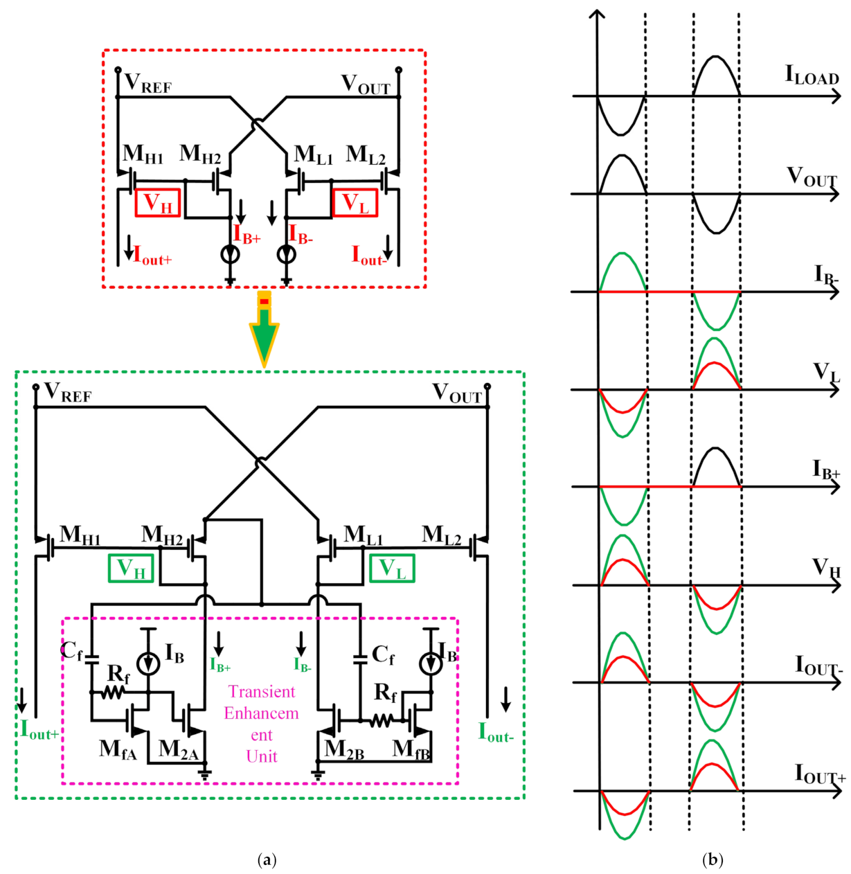
Figure 3.
The output currents of the Gm cells with TEU and without TEU.

Figure 4.
(a) Classical current mirror (CM); (b) Nonlinear current mirror.

Figure 5.
DC responses of the classical current mirror and the nonlinear current mirror.

Figure 6.
Transistor level schematic of the proposed OCL-LDO.
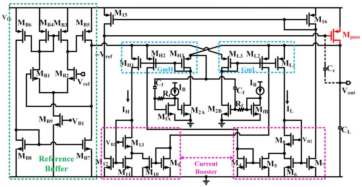
Figure 7.
Small signal block diagram of the proposed OCL-LDO.
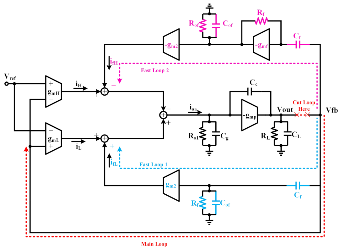
Figure 8.
(a) Loop gain of the proposed OCL–LDO under different load conditions with CL = 100 pF; (b) Loop gain versus load current, temperature, and process corner.
Figure 8.
(a) Loop gain of the proposed OCL–LDO under different load conditions with CL = 100 pF; (b) Loop gain versus load current, temperature, and process corner.

Figure 9.
(a) Monte Carlo simulation results of the phase margin with Iload = 10 μA and CL = 100 pF; (b) Monte Carlo simulation results of the phase margin with Iload = 100 mA and CL = 100 pF.
Figure 9.
(a) Monte Carlo simulation results of the phase margin with Iload = 10 μA and CL = 100 pF; (b) Monte Carlo simulation results of the phase margin with Iload = 100 mA and CL = 100 pF.

Figure 10.
Layout of the proposed OCL–LDO.

Figure 11.
(a) Simulated load regulation for Vin = 1.2 V, Vin = 1.5 V, and Vin = 1.8 V when VOUT = 1 V; (b) Simulated line regulation for different load currents (from 1 μA to 100 mA) when VOUT = 1 V.
Figure 11.
(a) Simulated load regulation for Vin = 1.2 V, Vin = 1.5 V, and Vin = 1.8 V when VOUT = 1 V; (b) Simulated line regulation for different load currents (from 1 μA to 100 mA) when VOUT = 1 V.
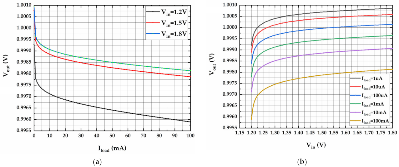
Figure 12.
Simulated PSR versus frequency under different load currents when VIN = 1.2 V, Vout = 1.0 V.
Figure 12.
Simulated PSR versus frequency under different load currents when VIN = 1.2 V, Vout = 1.0 V.

Figure 13.
Simulated load transient response of the OCL–LDO with/without TEU and CB.
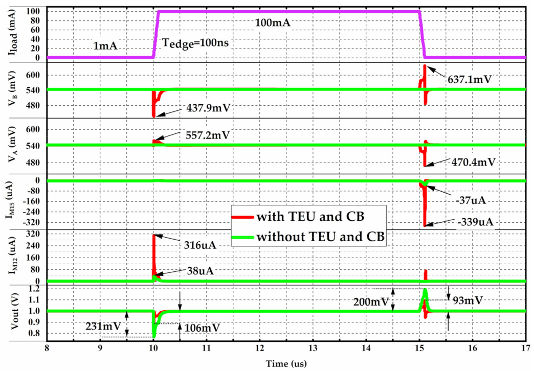
Figure 14.
Simulated line transient response of the proposed OCL–LDO.


Table 1.
Zeros and poles summary.
| Zeros | Poles |
|---|---|
Table 2.
Performance summary and comparison with state-of-the-art OCL-LDOs.
| [6] | [14] | [16] | [17] | [18] | [19] | [20] | This Work | |
|---|---|---|---|---|---|---|---|---|
| Year | 2013 | 2014 | 2017 | 2018 | 2020 | 2021 | 2021 | 2021 |
| Technology (nm) | 350 | 65 | 180 | 130 | 65 | 130 | 180 | 180 |
| Chip Area (mm2) | 0.04 | 0.0133 | 0.033 | 0.0252 | 0.01 | 0.029 | 0.103 | 0.01524 |
| Input Voltage (V) | 1.2–1.5 | 0.75–1.2 | 1.8 | 1.4–2.7 | 1.05–1.2 | 1.2 | 1.297–3.3 | 1.2–1.8 |
| Output Voltage (V) | 1.0–1.3 | 0.55 | 1.6 | 1.2–2.5 | 0.9 | 1 | 1.2 | 1 |
| Maximum Output Current (mA) | 100 | 50 | 100 | 50 | 20 | 50 | 50 | 100 |
| Quiescent Current (μA) | 1.2–14 | 15.9–487 | 71–101 | 65.8 | 65 | 95 | 8.6 | 10.3 |
| Current Efficiency (%) | 99.99 | 99.03 | 99.93 | 99.87 | 99.68 | 99.81 | 99.99 | 99.99 |
| Load Regulation (mV/mA) | - | 0.18 | N/A | 0.048 | - | 0.009 | 0.006 | 0.034 |
| Line Regulation (mV/V) | - | 4 | 131 | 1.23 | - | 5 | 0.065 | 2.74 |
| On-chip Capacitor (pF) | 0 | 4.1 | 12.7 | 2.6 | 1.4 | 10 | 6.1 | 7.5 |
| Output Capacitor (pF) | 0–100 | 470–10000 | 100 | 0–100 | 0–100 | 0–2000 | 0–50 | 0–100 |
| Settling Time (μs) | 2.7 | 0.25 | 0.2 | 0.69 | 0.3 | 0.2 | 3.6 | 0.19 |
| FOM (ns) | 0.0324 | 0.0795 | 0.202 | 0.90804 | 0.975 | 0.38 | 0.310 | 0.01957 |
Publisher’s Note: MDPI stays neutral with regard to jurisdictional claims in published maps and institutional affiliations. |
© 2022 by the authors. Licensee MDPI, Basel, Switzerland. This article is an open access article distributed under the terms and conditions of the Creative Commons Attribution (CC BY) license (https://creativecommons.org/licenses/by/4.0/).
Share and Cite
MDPI and ACS Style
Jiang, Y.; Wang, L.; Wang, S.; Cui, M.; Zheng, Z.; Li, Y. A Low-Power, Fast-Transient Output-Capacitorless LDO with Transient Enhancement Unit and Current Booster. Electronics 2022, 11, 701. https://doi.org/10.3390/electronics11050701
AMA Style
Jiang Y, Wang L, Wang S, Cui M, Zheng Z, Li Y. A Low-Power, Fast-Transient Output-Capacitorless LDO with Transient Enhancement Unit and Current Booster. Electronics. 2022; 11(5):701. https://doi.org/10.3390/electronics11050701
Chicago/Turabian StyleJiang, Yongchao, Lixin Wang, Shixin Wang, Mengyao Cui, Zhuoxuan Zheng, and Yuanzhe Li. 2022. "A Low-Power, Fast-Transient Output-Capacitorless LDO with Transient Enhancement Unit and Current Booster" Electronics 11, no. 5: 701. https://doi.org/10.3390/electronics11050701
Note that from the first issue of 2016, this journal uses article numbers instead of page numbers. See further details here.