
A 12-Bit, 100 MS/s SAR ADC Based on a Bridge Capacitor Array with Redundancy and Non-Linearity Calibration in 28 nm CMOS

State-Key Laboratory of ASIC and System, Fudan University, Shanghai 201203, China
*
Authors to whom correspondence should be addressed.
Electronics 2022, 11(5), 705; https://doi.org/10.3390/electronics11050705
Submission received: 4 February 2022
/
Revised: 19 February 2022
/
Accepted: 21 February 2022
/
Published: 25 February 2022
Abstract
:This paper presents a 12-bit, 100 MS/s successive approximation register (SAR) analog-to-digital converter (ADC) based on a bridge capacitor array with redundancy and non-linearity calibration. The differential non-linearity calibration method was proposed to compensate for the linearity, which is degraded by the parasitic capacitance of the bridge capacitor. To reduce the power dissipation and alleviate the settling error of the DAC capacitor array, a hybrid redundant scheme was proposed. A low-power, high-performance SAR ADC was implemented based on the proposed techniques. This SAR ADC prototype was implemented in 28 nm CMOS technology. Measurement results showed that the proposed SAR ADC could achieve a (signal-to-noise distortion ratio) SNDR of 61.46 dB and 58.82 dB at low and Nyquist input frequencies, respectively, resulting in figure of merits (FOMs) of 8.69 fJ/conversion and 11.8 fJ/conversion step, respectively. The SAR ADC core occupied an active area 0.0227 mm2.
1. Introduction
The successive approximation register (SAR) analog-to-digital converter (ADC) is very popular because it can achieve low power and high performance at 100 MS/s with 10 to 13 bits [1,2,3,4,5,6,7,8,9,10]. With the feature sizes of CMOS devices scaled down, the power supply voltage becomes lower and lower, which is not conducive to analog circuits such as high-performance operational amplifiers as the low power supply voltage limits the output swing and gain of the amplifier. However, there are very few analog circuits in a SAR ADC. The SAR ADC is mainly composed of the dynamic comparator, the DAC capacitor array and the digital control logic, which is compatible with advanced CMOS processes.
For an N-bit SAR ADC, the conventional binary-weighted DAC array requires 2N unit capacitors. The number of unit capacitors increases exponentially with N and they occupy a large area, causing large interconnection parasitism. In addition, the mismatch between the LSB capacitor and MSB capacitor also becomes larger. These adverse factors affect the speed, power dissipation and accuracy of an ADC. A DAC based on a bridge-capacitor array can greatly reduce the number of unit capacitors, which is beneficial to its speed and power. However, the bridge capacitor can cause parasitic capacitance in a DAC, which affects the harmonic distortion and signal-to-noise ratio (SNR). Moreover, the bridge capacitor is not an integer, which is not conducive for matching the layout. An integer bridge capacitor was introduced in [11] to reduce mismatch with other unit capacitors. However, there was still parasitic capacitance in this integer bridge capacitor. Some calibration methods were proposed to compensate for the parasitic capacitance of the bridge capacitor. Histogram-based ratio-mismatch calibration for the bridge DAC is proposed in [12], which required a complex digital circuit and took much time to converge. The uniform quantization theory-based linearity calibration was introduced in [13], which needed an input signal to satisfy the prerogative of quantization theory. The weighting of the capacitors in an MSB array of a bridge DAC was calibrated by the successive approximation method in [14]. However, the error of weighting in the capacitors in an LSB array affects the result of the calibration. Although dynamic element matching (DEM) [15] can reduce the mismatch between unit capacitors and improve linearity, it can not improve the SNR.
With the continuous improvement of the ADC sampling rate, the setting issue of a DAC capacitor array becomes serious, which can result in an incorrect comparison because the reference voltage does not recovered to its initial value before the comparator starts comparing. In order to achieve a settling error within 0.5 LSB, the driving switches should be designed with a stronger driving ability, which consumes more power. Moreover, larger driving switches introduce more parasitic capacitance, which reduces the speed of the ADC. The redundancy can alleviate the settling error of a DAC [16,17,18,19,20,21,22,23,24,25,26,27,28]. The non-binary redundancy [29] needs a complex digital control circuit and an extra an ROM. Moreover, non-binary redundancy makes the floorplan of the layout of a DAC capacitor array difficult, which degrades the matching of the unit capacitors. When the DAC settling error is within the redundancy range, the wrong comparison can be corrected by the binary-scaled-error method [30]. However, introduced capacitors will reduce the quantization range. The capacitors in an MSB array and LSB array of a bridge DAC capacitor array are split respectively [31,32] and the redundancy can be introduced. However, there is no redundancy for the MSB capacitor in an LSB array, which still produces the settling error.
This paper proposes the differential non-linearity calibration method to compensate for the linearity that is degraded by the parasitic capacitance of the bridge capacitor in a DAC capacitor array. Moreover, in order to alleviate DAC settling error and reduce the power, a hybrid redundancy scheme is proposed.
The rest of this article is organized as follows. Section 2 describes the overall architecture of the proposed SAR ADC. The proposed differential non-linearity calibration method and the hybrid redundancy scheme are presented in Section 3. The circuit implementation of the key building blocks is presented in Section 4. Measurement results are presented in Section 5. Finally, Section 6 concludes the paper.
2. SAR ADC Overall Architecture
The overall architecture of the proposed SAR ADC is presented in Figure 1. The bridge DAC capacitor array consists of an 8-bit MSB array and a 4-bit LSB array, which can reduce the number of unit capacitors. The MSB arrays are the M-bit DAC capacitor array and the LSB arrays are the L-bit DAC capacitor array. When M > N, the influence of the parasitic capacitance in the LSB arrays on the linearity of the SAR ADC will be reduced [33]. As a result, we chose M = 8 and L = 4. An integer bridge capacitor Ca was adopted, which was conducive to matching the layout. Successive approximation register (SAR) logic was used to generate and control the signals Dp<15:0> and Dn<15:0>, which could control switches Sp0–Sp14 and Sn0–Sn14 according to the OUTp and OUTn of the comparator output. Digital error correction (DEC) could convert the original 16-bit digital codes to 12-bit binary codes. A calibration capacitor array was used to compensate for the linearity, which was degraded by the parasitic capacitance of the bridge capacitor Ca. The calibration circuit and logic provided the calibration clock CLKcali for the dynamic comparator CMP and the thermometer code thc<14:0> for the calibration capacitor array. The clock driver generated the sampling clock CLK and calibration clock CLK_cali_logic.
3. The Proposed Differential Non-Linearity Calibration Method and Hybrid Redundancy Scheme
3.1. Analysis of Parasitic Capacitance in the Bridge DAC Capacitor Array
Although a bridge DAC capacitor array can reduce the number of unit capacitors, the parasitic capacitance of the bridge capacitor influences the linearity of the SAR ADC. Figure 2 shows a 12-bit bridge DAC capacitor array with parasitic capacitance Cp1 and Cp2. The capacitance Cp2 is composed of the parasitic capacitance from the top plate to the ground of capacitors C4 to C11 and Ca. The capacitance Cp1 is composed of the parasitic capacitance from the top plate to the ground of capacitors C0 to C3 and the parasitic capacitance from the bottom plate to the ground of the capacitor Ca.
In order to reduce the charge injection, bottom-plate sampling was adopted. The purple capacitor C4 was put into the MSB array and it only participated in the sampling process, it did not participate in the quantization process. Only the MSB array samples input the signal Vin, which could reduce input load capacitance. During the sampling period switches S1, S2 and S3 were on. The top plates and bottom plates of capacitors C11 to C4 in the MSB array were connected to Vcm and the input signal Vin, respectively. The top plates and bottom plates of capacitors C0 to C3 were connected to Vcm and the ground, respectively. The charge QX at the node X could be expressed as follows:
The charge QY at the node Y could be expressed as follows:
In the quantization process, it was assumed that M unit capacitors were connected to Vref in the MSB array and N unit capacitors were connected to Vref in the LSB array. The voltage of the nodes X and Y were VX and VY, respectively. At this time, the charge QX at the node X could be expressed as follows:
The charge QY at the node Y could be expressed as follows:
In the process of charge distribution, the charges QX and QY at the nodes X and Y, respectively, remained unchanged. As a result, Equations (5) and (6) could be obtained.
Combining Equations (5) and (6), the voltage VX at the node X is shown as:
As can be seen from Equations (7) and (8), the parasitic capacitor Cp2 only appeared on the denominator and did not affect the linearity of the ADC. However, the parasitic capacitor Cp1 appeared on both the numerator and denominator, which affected the linearity of the ADC.
In Equation (7), assuming that Cp1 = 0, Ca= 3 Cu and Cdum = 30 Cu, Equation (9) could be obtained. In Equation (10), b = 25 M + 2 N. In this case, the DAC capacitor array had correct scaling. However, the parasitic capacitor Cp1 could not be ignored. In Equation (7), if the capacitor Cdum was programmable, the influence of the capacitor Cp1 on the linearity could have adjusted the capacitor Cdum.
3.2. The Proposed Differential Non-Linearity Calibration Method
In order to keep the correct scaling of the DAC capacitor array, the sum of the weighting of all capacitors in the LSB array should have been equal to the weighting of the lowest bit in the MSB array. Figure 3 shows the DAC capacitor array during calibration. When CLK was high, switches S0 and S1 were on. The bottom plates and top plates of the capacitors C4 to C11 in the MSB array were connected to the ground and Vcm, respectively. The bottom plates and top plates of capacitors C0 to C3 were connected to Vref and Vcm, respectively. When CLK was low, switches S0 and S1 were off. The bottom plates of capacitors C0 to C3 were connected to the ground in the LSB array. The bottom plates of capacitors C6 to C11 and C4 were still connected to the ground and the bottom plate of capacitor C5 was connected to Vref. The charges QX and QY of the nodes X and Y, respectively, were unchanged during (a) and (b) in Figure 3. As a result, Equations (11) and (12) could be obtained.
Combining Equations (11) and (12), the voltage VX at the node X is shown as:
When the sum of all the weighting of the capacitors in the LSB array was equal to the weighting of the capacitor C5 in the MSB array, the voltage VX at the node X was equal to Vcm in Figure 3b. In Equation (13), Vx = Vcm and Vref = 2V cm, the programmable capacitor Cdum is shown as:
The voltage VX at the node X varied with the capacitor Cdum. When the value of the capacitor Cdum was appropriate, the voltage VX = Vcm at the node X. Therefore, the capacitor Cdum could have been adjusted according to whether the voltage VX at the node X was equal to Vcm.
The proposed differential non-linearity calibration method is shown in Figure 4. The initial value of the capacitor Cdum was smaller than that in Equation (14) in Figure 4. The first step of the proposed differential non-linearity calibration method was to set the initial voltage value of the MSB array and the LSB array. In Figure 4a, CLK = 1 and switches S0 to S3 were on. In the upper capacitor array, the bottom plates of capacitors C6 to C11 and C0 to C4 were connected to the ground, and the bottom plate of capacitor C5 was connected to Vref. In the lower capacitor array, the bottom plates of capacitors C4 to C11 were connected to the ground, and the bottom plates of capacitors C0 to C3 were connected to Vref. The second step of the calibration was the charge redistribution. In Figure 4b, CLK = 0 and switches S0 to S3 were off. In the upper capacitor array, the bottom plates of capacitors C4 to C11 were connected to the ground, and the bottom plates of capacitors C0 to C3 were connected to Vref. In the lower capacitor array, the bottom plates of capacitors C6 to C11 and C0 to C4 were connected to the ground, and the bottom plates of capacitor C5 was connected to Vref. The value of the capacitor Cdum was smaller than the ideal value. Therefore, the voltage VX at the node X was smaller than Vcm and the voltage VM at the node M was larger than Vcm in Figure 4b according to Equation (13). The voltage VX increased and voltage VM decreased as the capacitance value of the capacitor Cdum increased.
The programmable capacitor Cdum is shown in Figure 5 and was composed of the fixed capacitor Cfixed and the adjustable capacitor Cadjust. In Figure 5, the capacitance value of the capacitor Cfixed= 26 Cu. The capacitor Cadjust was composed of eight cells. Each cell consisted of two unit capacitors Cu and two switches. When S0 was on and S1 was off, two unit capacitors Cu were connected in series and the capacitance value of the cell was 0.5 Cu. When S0 and S1 were on, the capacitance value of the cell was Cu. As a result, the capacitance value of capacitors Cadjust and Cdum ranged from 0.5 Cu to 8 Cu and from 26.5 Cu to 34 Cu, respectively.
The capacitance value of Cadjust needed to change continuously in steps of 0.5 Cu. As a result, the switches S0 to S14 could be controlled by the 15-bit thermometer code. The calibration circuit of the non-linearity is shown in Figure 6. CLKcali is the calibration clock for the comparator. The binary-to-thermometer converter converts 4-bit binary codes b<0:3> to 15-bit thermometer codes thc<0:14>, which were used to control switches S0 to S14 of capacitor Cdum in the LSB array. The comparator compared voltages VM and VX at nodes M and X, respectively. When the voltage VX >VM, the cali_control_cell block generated cal_finish to stop the 4-bit counter counting and stored thc<0:14> into the D-type flip flops. At this point, the calibration was complete.
3.3. The Proposed Hybrid Redundancy Method
Figure 7a shows the concept of the conventional binary search algorithm. There was a 4-bit case. Vref is the reference voltage. Vin is the input signal. Firstly, Vin was sampled on the top plates of the capacitor arrays. After that, the comparator started the first comparison. According to the first comparison, the voltage difference of the two DACs added or subtracted 1/2 Vref. The conversion repeated until the last bit was decided. In order to obtain correct digital output codes, the DAC settling error had to be less than 1/2 LSB. If a wrong decision was produced before the last comparison, even if the remaining decisions were correct, the voltage difference between the input signal and reference voltage in the last cycle was larger than LSB, which degraded the performance of the SAR ADC.
Figure 7b shows the example of the binary-scaled error compensation algorithm [30], there was also a 4-bit case. A compensative capacitor was inserted in the DAC capacitor array. Therefore, it needed 5-bit cycles to finish the conversion in this 4-bit example. After the first comparison, the number of possible quantization levels was reduced from 16 to 8. Hence, the effective input range of the binary-scaled error compensation method was reduced by a factor of 2. In Figure 7b, a wrong decision was made in the second cycle. After the fourth cycle, the input range did not reduce but shifted to compensate for the error. If the decisions were correct from the third cycle to the fifth cycle, it was possible to obtain a correct digital output code. There were multiple digital codes representing the same input voltage because of extra compensative cycles; therefore, a certain range error could be tolerated. However, extra compensative capacitors increased the sampling capacitance and resulted in a smaller input range. Moreover, it was not suitable for the bridge capacitor array.
The methods in [30,31] were not suitable for the bridge structure. In order to adapt to the bridge structure, hybrid redundancy based on the bridge capacitor array was proposed. Figure 8 is the conventional bridge capacitor array of the 12-bit SAR ADC. There was no any redundancy in the bridge capacitor array. Therefore, it did not tolerate the DAC settling error.
In [31], the binary-scaled recombination method was used in the higher DAC and the lower DAC to tolerate the DAC settling error in Figure 9. The weighting of C6 was 32 LSBs, the sum of all weightings of capacitors in the lower DAC was 31 LSBs. The weighting of C6 was larger than the sum of the weightings of capacitors in the lower DAC. Therefore, there was no redundancy. If a wrong decision was made in the last comparison cycle inthe higher DAC, it would produce a wrong digital output code.
Figure 10 shows the proposed hybrid redundancy based on the bridge capacitor array. In the higher DAC, the binary-scaled recombination method was used. The MSB capacitor was split into two groups: 56 Cu and 8(23)Cu. Next, 8(23)Cu was split into 2(21)Cu, 2(21)Cu, 2(21)Cu, 1(20)Cu and 1(20)Cu, respectively. Those groups were added to other groups or inserted into the higher DAC. In the lower DAC, binary-scaled compensation was used. Capacitors C5 and C2 were inserted into the lower DAC to compensate for error. In order to keep the linearity of the DAC, capacitor C5 and C2 were split from capacitor Cdum; hence, the capacitance of capacitor Cdum was reduced from 30 Cu to 20 Cu. In Figure 10, the weighting of capacitor C7 was 32 LSBs, the sum of all weightings of the capacitors in the lower DAC was 51 LSBs. The weighting of C7 was smaller than the sum of all weightings of capacitors in the lower DAC. Therefore, there was redundancy. If a wrong decision was made in the last cycle in the higher DAC, it was possible to produce a correct digital output code. Moreover, the inserted capacitors were from capacitor Cdum, which neither increased the sampling capacitance nor reduced the input range.
Table 1 shows the comparison of redundant ranges with different redundant methods. In the 8th cycle (the last cycle of the higher DAC), the redundant range was 0 LSB in [32]. In the 10th cycle (the last cycle of the higher DAC), the redundant range was 20 LSBs. The weighting of the last cycle of the higher DAC was relatively large. If a wrong decision was made in this cycle, the performance of the ADC would degrade. The proposed hybrid redundancy could provide a certain range of redundancy to tolerate the DAC settling error in this cycle. There was no redundancy in the 6th to 8th cycles in the higher DAC in [32]. There was a certain range of redundancy for each cycle in the higher DAC in the proposed hybrid redundancy method. Moreover, the redundant range of each cycle in the proposed hybrid was lager than the redundant range in [32]. Therefore, the proposed hybrid redundancy was suitable for the bridge structure and the high-resolution ADC.
The digital output could be expressed as:
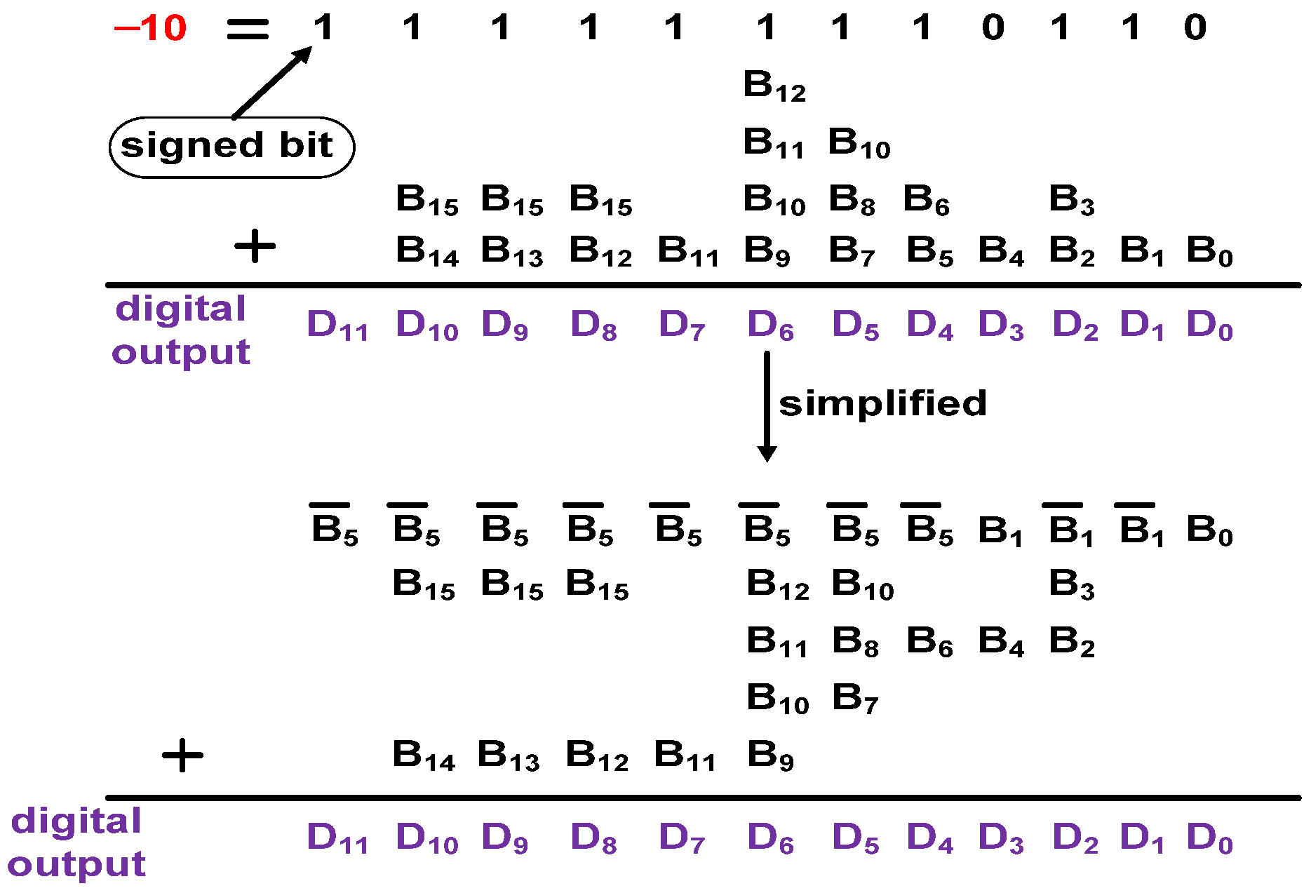
Figure 11 illustrates the digital error correction logic, which converted the 16-bit redundant codes to 12-bit binary codes. The digital codes has an offset of 10, and the offset was moved by logic operations.
4. The Implementation of Key Building Blocks
4.1. Bootstrapped Switch
Bootstrapped switch [34] is shown in Figure 12. CLKs was the sampling clock. When CLKs = 0, transistors M7 and M8 discharged node A to the ground. Transistor M4 charged capacitor Cs to VDD. Transistors M9 and M10 were off. At this time, the bootstrapped switches were in the hold state. When CLKs = 1, transistors M1 and M8 were off and transistor M6 was on. The gate and source of transistor M10 were connected to the top plate and the bottom plate of capacitor Cs. Therefore, the gate-to-source voltage of transistor M10 was VDD. At this time, the bootstrapped switches were in the tracking state. When CLKs = 0, transistor M10 was off. However, the input signal Vin was fed through the output Vout by the parasitic capacitance Cds of transistor M10, which affected the spurious-free dynamic range (SFDR). Transistor M10-dum was the dummy transistor of M10, and the gate of transistor M10-dum was connected to the ground. The input signal Vip was the differential signal of the input signal Vin, which could cancel the feedthrough of Vin by the parasitic capacitance Cds of transistor M10-dum.
4.2. Dynamic Comparator
Figure 13 shows a dynamic three-stage comparator [35]. When CLks = 1 and CLKsn = 0, transistors M3 and M4 charged nodes A and B to VDD, transistors M5 and M6 discharge the nodes C and D to the ground and transistors M15 and M16 charged nodes E and D to VDD. Outputs OUTn and OUTp were VDD. Transistors M0, M9 and M10 were off. At this time, the comparator was in the reset state. When CLKs = 0 and CLKsn = 1, the dynamic comparator started comparing the differential input signals Vin and Vip. A three stage dynamic comparator had lower input noise, offset voltage and faster speed.
4.3. Asynchronous Dynamic Control Logic
Figure 14 shows asynchronous control logic, which was composed of 19 D-type flip flops (DFFs). For the DFFs, when Set = 0, output Q of the DFFs was VDD. When Reset = 0, output Q of the DFFs was ground. Valid represents the state of the comparator. When valid was high, the comparator was in the reset state. When valid was low, the comparator was comparing the input signals. Figure 15 shows the timing of the asynchronous control logic. The extra cycle A was used for charge redistribution because bottom-plate sampling was adopted.
Figure 16 shows the DAC control logic. OUTp and OUTn were outputs of the comparator. CLK<i> stands for one of CLK0 to CLK15 in Figure 15. When the ADC was sampling, the CLKs = 1 and CLK<i> = 0. At this time, transistor M1 was off and transistor M2 charged node A to VDD. Transistor M3 was off and transistor M4 discharged node B to the ground; therefore, Out<i> was ground and Out<i> was connected to the bottom plate of each capacitor in the differential DAC capacitor arrays. When CLKs = 1 and CLK<i> = 1, transistor M1 was on and transistor M2 was off. Transistors M5 and M6 were off. At this time, Out<i> changed with Outp or Outn. When Outp or Outn was VDD, Out<i> was still ground. When Outp or Outn was ground, transistor M3 charged node B to VDD and Out<i> was VDD.
4.4. Capacitor Array
The DAC capacitor array had a great impact on the performance of the SAR ADC. The mismatch of the unit capacitor could affect the SFDR and SNDR. Figure 17a shows the structure of the unit capacitor. The top plate was the middle and the bottom plates were on both sides. The unit capacitor was composed of metal3, metal4 and metal5: three layers of metal. Each metal capacitor was the interdigital capacitor. Figure 17b shows the floorplan the DAC capacitor array. The top plates of capacitors Ci + 1,Ci and Ci − 1 were connected together. Bottom plates Sj + 1, Sj and Sj − 1 were connected to different control signals. In Figure 17b, only two unit capacitors were placed in each column. In the actual layout, four or eight unit capacitors could be placed in each column according to requirements. The active area of the unit capacitor was 2.045 um × 1.85 um. The value of the unit capacitor was 6fF.
4.5. Clock Driver
The clock driver could convert the differential sinusoidal signals into square waves, which could be used as the sampling clock. Figure 18 shows the clock driver. The capacitor C1 and resistor R1 and capacitor C2 and resistor R2 constituted high pass filters, respectively. Resistors R3 and R4 provided suitable static operating points for the differential input transistors M1 and M2. The resistors M5 and M6 formed the common mode feedback circuit, which could stabilize the output voltage of the first stage. Moreover, resistors M3 and M4 could provide appropriate bias voltage for transistors M3 and M4. The first stage was the differential amplifier, and the second stage converted differential signals to a single ended signal. The inverter converted the single ended signal into a square wave.
4.6. Post Simulation
Figure 19 shows the post simulation results of SNDR with temperature and corner when the input frequency was 49.96 MHz. As can be seen from Figure 19, SNDR also increased with the increase in temperature. When the temperature was 120 °C and corner was ff, SNDR reached a maximum of 65.03 dB. When the temperature was −40 °C and corner was ss, SNDR reached a minimum of 57.75 dB.
5. Measurement Results
The prototype was fabricated using 1P8M 28 nm CMOS technology. The chip photograph and proposed SAR ADC are as shown in Figure 20. The active area of the proposed SAR ADC was 303 um × 75 um.
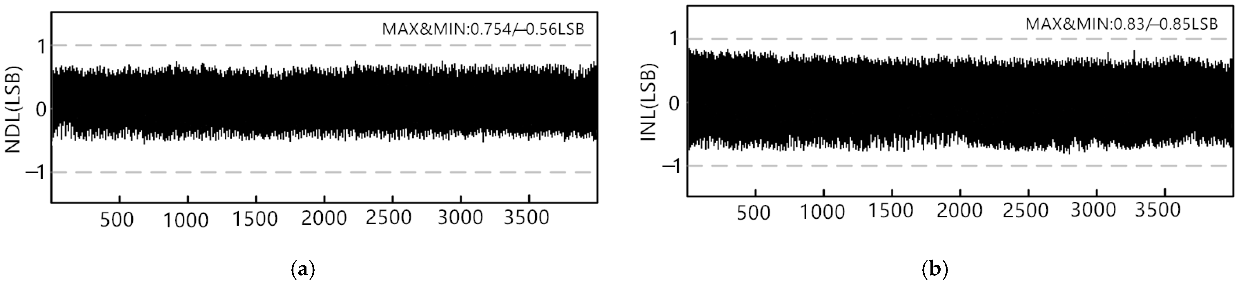
Figure 21a shows the measured spectrum with inputs at 4.89 MHz when the proposed calibration method was off. The measured SFDR and SNDR were 79.5 dB and 58.16 dB, respectively. Figure 21b shows the measured spectrum when the proposed calibration method was on. The measured SFDR and SNDR were 82.7 dB and 61.46 dB, respectively. When proposed, the calibration method was on and the SFDR and SNDR were increased by 3.2 dB and 3.3 dB, respectively. Figure 22a shows the measured spectrum with inputs at 49.96 MHz when the proposed calibration method was off. The measured SFDR and SNDR were 77.5 dB and 56.3 dB, respectively. Figure 22b shows the measured spectrum when the proposed method was on. The measured SFDR and SNDR were 79.1 dB and 58.82 dB. respectively. When the proposed calibration method was on, the SFDR and SNDR were increased by 1.6 dB and 2.52 dB, respectively. Figure 23 shows the measured DNL and INL when the proposed calibration method was off. The peak DNL and INL were 1.40/−1.23 LSB and 1.43/−1.35 LSB, respectively. Figure 24 shows the measured DNL and INL when the proposed calibration method was on. The peak DNL and INL were 0.754/−0.56 LSB and 0.83/−0.85 LSB, respectively.
The proposed calibration method was helpful for improving static and dynamic performance.
The power consumption of the proposed SAR ADC was 0.86 mW. The proposed SAR ADC achieved a figure of merit (FOM) of 8.69 and 11.8 fJ/conversion step at low-frequency input and Nyquist input frequency, respectively.
6. Conclusions
In this paper, a 12-bit, 100 MS/s SAR ADC with calibration is proposed. The differential non-linearity calibration method was proposed to compensate for the linearity, which was degraded by the parasitic capacitance of the bridge capacitor. To reduce the power dissipation and alleviate the settling error of the DAC capacitor array, a hybrid redundant scheme was proposed. The proposed SAR ADC consumed 0.86 mW. The ADC achieved an SNDR of 61.46 dB and 58.82 dB at low and Nyquist input frequencies, respectively, resulting in FoMs of 8.69 and 11.8 fJ/conversion step, respectively. The FOM [40] is shown as Equation (17):
In Equation (17), sampling frequency was represented by fs, power consumption of the SAR ADC was presented by Power, effective resolution bandwidth was represented by ERBW and the effective number of bits of the ADC was represented by ENOB.
Author Contributions
Research methodology, Y.Z., F.Y.; circuit design, Y.Z.; layout drawing, Y.Z.; writing—original draft preparation, Y.Z., F.Y.; supervision, J.R.; validation, Y.Z., F.Y. All authors have read and agreed to the published version of the manuscript.
Funding
This work was supported by the National Key Research and Development Program of China under Grant 2020YFC0122100.
Data Availability Statement
Data are contained within the article. The data presented in this study are available in this paper.
Conflicts of Interest
The authors declare no conflict of interest.
References
- Liu, C.-C.; Huang, M.-C.; Tu, Y.-H. A 12 bit 100 MS/s SAR-Assisted Digital-Slope ADC. IEEE J. Solid-State Circuits 2016, 51, 2941–2950. [Google Scholar] [CrossRef]
- Tseng, W.; Lee, W.; Huang, C.; Chiu, P. A 12-bit 104 MS/s SAR ADC in 28 nm CMOS for Digitally-Assisted Wireless Transmitters. IEEE J. Solid-State Circuits 2016, 51, 2222–2231. [Google Scholar] [CrossRef]
- Luu, D.; Kull, L.; Toifl, T.; Menolfi, C.; Brandli, M.; Francese, P.A.; Morf, T.; Kossel, M.; Yueksel, H.; Cevrero, A.; et al. A 12-bit 300-MS/s SAR ADC With Inverter-Based Preamplifier and Common-Mode-Regulation DAC in 14-nm CMOS FinFET. IEEE J. Solid-State Circuits 2018, 53, 3268–3279. [Google Scholar] [CrossRef]
- Li, M.; Chen, Y.; Ye, F.; Ren, J. A 100MS/S 12-bit Coarse-Fine SAR ADC with Shared Split-CDAC. In Proceedings of the 2018 IEEE International Symposium on Circuits and Systems (ISCAS), Florence, Italy, 27–30 May 2018; pp. 1–4. [Google Scholar]
- Lan, Z.; Dong, L.; Jing, X.; Geng, L. A 12-Bit 100MS/s SAR ADC with Digital Error Correction and High-Speed LMS-Based Background Calibration. In Proceedings of the 2021 IEEE International Symposium on Circuits and Systems (ISCAS), Daegu, Korea, 22–28 May 2021; pp. 1–5. [Google Scholar]
- Wang, Q.; Zhou, L.; Peng, Z.; Li, N.; Wang, Z. A 12-b 100MS/s low-power successive approximation register ADC in 65nm COMS. In Proceedings of the 2014 IEEE International Conference on Electron Devices and Solid-State Circuits, Barcelona, Spain, 5 May 2014; pp. 1–2. [Google Scholar]
- Du, L.; Wu, S.; Jiang, M.; Ning, N.; Yu, Q.; Liu, Y. A 10-bit 100MS/s subrange SAR ADC with time-domain quantization. In Proceedings of the 2014 IEEE International Symposium on Circuits and Systems (ISCAS), Melbourne, Australia, 1–5 June 2014; pp. 301–304. [Google Scholar]
- Zheng, Y.; Lan, J.; Ye, F.; Ren, J. A 68.36 dB 12 bit 100MS/s SAR ADC with a low-noise comparator in 14-nm CMOS FinFet. In Proceedings of the 14th International Conference on ASIC (ASICON), Kunming, China, 26–29 October 2021; pp. 1–4. [Google Scholar]
- Zhang, B.; Yao, B.; Liu, L.; Wu, N. A 10-bit 100-MS/s power-efficient asynchronous SAR ADC. In Proceedings of the 13th IEEE International Conference on Solid-State and Integrated Circuit Technology (ICSICT), Hangzhou, China, 25–28 October 2016; pp. 722–724. [Google Scholar]
- Wu, S.Y.; Du, L.; Jiang, M.; Ning, N.; Yu, Q.; Liu, Y. A 10-bit 100MS/s time domain Flash-SAR ADC. In Proceedings of the 2014 IEEE International Conference on Electron Devices and Solid-State Circuits, Chengdu, China, 18–20 June 2014; pp. 1–2. [Google Scholar]
- Agnes, A.; Bonizzoni, E.; Malcovati, P.; Maloberti, F. A 9.4-ENOB 1V 3.8μW 100kS/s SAR ADC with Time-Domain Comparator. In Proceedings of the IEEE International Solid-State Circuits Conference—Digest of Technical Papers, San Francisco, CA, USA, 3–7 February 2008; pp. 246–610. [Google Scholar]
- Zhu, Y.; Chan, C.-H.; Wong, S.-S.; Seng-Pan, U.; Martins, R.P. Histogram-Based Ratio Mismatch Calibration for Bridge-DAC in 12-bit 120 MS/s SAR ADC. IEEE Trans. Very Large Scale Integr. Syst. 2016, 24, 1203–1207. [Google Scholar] [CrossRef]
- Liu, J.; Zhu, Y.; Chan, C.-H.; Sin, S.-W.; U, S.-P.; Martins, R.P.D.S. Uniform Quantization Theory-Based Linearity Calibration for Split Capacitive DAC in an SAR ADC. IEEE Trans. Very Large Scale Integr. Syst. 2016, 24, 2603–2607. [Google Scholar] [CrossRef]
- Ye, F.; Li, S.; Zhu, M.; Ni, Z.; Ren, J. A 13-bit 180-MS/s SAR ADC with Efficient Capacitor-Mismatch Estimation and Dither Enhancement. In Proceedings of the 2019 IEEE International Symposium on Circuits and Systems (ISCAS), Sapporo, Japan, 26–29 May 2019; pp. 1–4. [Google Scholar]
- Chan, K.L.; Rakuljic, N.; Galton, I. Segmented Dynamic Element Matching for High-Resolution Digital-to-Analog Con-version. IEEE Trans. Circuits Syst. I Regul. Pap. 2008, 55, 3383–3392. [Google Scholar] [CrossRef]
- Chang, S.; Zhou, X.; Ding, Z.; Li, Q. A 12-bit 30MS/s SAR ADC with VCO-Based Comparator and Split-and-Recombination Redundancy for Bypass Logic. In Proceedings of the 2019 IEEE International Symposium on Circuits and Systems (ISCAS), Sapporo, Japan, 26–29 May 2019; pp. 1–5. [Google Scholar]
- Mei, Y.; Li, S. A 10-bit 100MS/s SAR ADC for the Hadronic Calorimeter Upgrade. In Proceedings of the 2019 IEEE National Aerospace and Electronics Conference (NAECON), Dayton, OH, USA, 15–19 July 2019; pp. 59–62. [Google Scholar]
- Okazaki, T.; Kanemoto, D.; Pokharel, R.; Yoshida, K.; Kanaya, H. A design technique for a high-speed SAR ADC using non-binary search algorithm and redundancy. In Proceedings of the Asia-Pacific Microwave Conference Proceedings (APMC), Seoul, Korea, 5–8 November 2013; pp. 506–508. [Google Scholar]
- Ogawa, T.; Kobayashi, H.; Hotta, M.; Takahashi, Y.; San, H.; Takai, N. SAR ADC algorithm with redundancy. In Proceedings of the APCCAS—IEEE Asia Pacific Conference on Circuits and Systems, Macau, China, 30 November–3 December 2008; pp. 268–271. [Google Scholar]
- Verma, D.; Rikan, B.S.; Shehzad, K.; Kim, S.J.; Khan, D.; Kommangun, V.; Ali Shah, S.A.; Pu, Y.; Yoo, S.-S.; Hwang, K.C.; et al. A Design of 44.1 fJ/Conv-Step 12-Bit 80 ms/s Time Interleaved Hybrid Type SAR ADC With Redundancy Capacitor and On-Chip Time-Skew Calibration. IEEE Access 2021, 9, 133143–133155. [Google Scholar] [CrossRef]
- Lopez-Angulo, A.; Gines, A.; Peralias, E. Digital calibration of capacitor mismatch and comparison offset in Split-CDAC SAR ADCs with redundancy. In Proceedings of the 18th IEEE International New Circuits and Systems Conference (NEWCAS), Online, 16–19 June 2020; pp. 130–133. [Google Scholar]
- Bunsen, K.; Martens, E.; Dermit, D.; Craninckx, J. A Redundancy-Based Background Calibration for Comparator Off-set/Threshold and DAC Gain in a Ping-Pong SAR ADC. IEEE Trans. Circuits Syst. II Express Briefs 2021, 68, 592–596. [Google Scholar] [CrossRef]
- Guerber, J.; Gande, M.; Venkatram, H.; Waters, A.; Moon, U.-K. A 10b Ternary SAR ADC with decision time quantization based redundancy. In Proceedings of the IEEE Asian Solid-State Circuits Conference, Jeju, Korea, 14–16 November 2011; pp. 65–68. [Google Scholar] [CrossRef]
- Chang, A.H.; Lee, H.-S.; Boning, D. A 12b 50MS/s 2.1mW SAR ADC with redundancy and digital background calibration. In Proceedings of the ESSCIRC (ESSCIRC), Bucharest, Romania, 16–20 September 2013; pp. 109–112. [Google Scholar]
- Gines, A.; Lopez-Angulo, A.; Peralias, E.; Rueda, A. Description of SAR ADCs with Digital Redundancy using a Unified Hardware-Based Approach. In Proceedings of the IEEE International Symposium on Circuits and Systems (ISCAS), Florence, Italy, 27–30 May 2018; pp. 1–5. [Google Scholar]
- Li, D.; Liu, M.; Zhao, L.; Mao, H.; Ding, R.; Zhu, Z. An 8-Bit 2.1-mW 350-MS/s SAR ADC With 1.5 b/cycle Redundancy in 65-nm CMOS. IEEE Trans. Circuits Syst. II Express Briefs 2020, 67, 2307–2311. [Google Scholar] [CrossRef]
- Haenzsche, S.; Hoppner, S.; Ellguth, G.; Schuffny, R. A 12-b 4-MS/s SAR ADC With Configurable Redundancy in 28-nm CMOS Technology. IEEE Trans. Circuits Syst. II Express Briefs 2014, 61, 835–839. [Google Scholar] [CrossRef]
- Zeloufi, M.; Dzahini, D. Design of low power and low area 12-bit 40MSPS SAR ADCs with a redundancy algorithm and digital calibration for high dynamic range calorimeter readout. In Proceedings of the 2016 IEEE Nuclear Science Symposium, Medical Imaging Conference and Room-Temperature Semiconductor Detector Workshop (NSS/MIC/RTSD), Strasbourg, France, 29 October–6 November 2016; pp. 1–7. [Google Scholar]
- Kuttner, F. A 1.2V 10b 20MSample/s non-binary successive approximation ADC in 0.13 μm CMOS. In Proceedings of the International Solid-State Circuits Conference—(ISSCC), San Francisco, CA, USA, 13 February 2003; Volume 1, pp. 176–177. [Google Scholar]
- Liu, C.-C.; Chang, S.-J.; Huang, G.-Y.; Lin, Y.-Z.; Huang, C.-M.; Huang, C.-H.; Bu, L.; Tsai, C.-C. A 10b 100MS/s 1.13mW SAR ADC with binary-scaled error compensation. In Proceedings of the 2010 IEEE International Solid-State Circuits Conference—(ISSCC), San Francisco, CA, USA, 7–11 February 2010; pp. 386–387. [Google Scholar]
- Zheng, Y.; Ye, F.; Ren, J. A 13 Bit 100 MS/s SAR ADC with 74.57 dB SNDR in 14-nm CMOS FinFET. In Proceedings of the 2020 IEEE International Symposium on Circuits and Systems (ISCAS), Online, 10–21 October 2020; pp. 1–4. [Google Scholar]
- Li, M.; Yao, Y.; Hu, B.; Wei, J.; Chen, Y.; Ma, S.; Ye, F.; Ren, J. A 6.94-fJ/Conversion-Step 12-bit 100-MS/s Asynchronous SAR ADC Exploiting Split-CDAC in 65-nm CMOS. IEEE Access 2021, 9, 77545–77554. [Google Scholar] [CrossRef]
- Fiorelli, R.; Guerra, O.; Del Rio, R.; Rodriguez-Vazquez, A. Effects of capacitors non-idealities in un-even split-capacitor array SAR ADCs. In Proceedings of the 2015 Conference on Design of Circuits and Integrated Systems (DCIS), Estoril, Portugal, 25–27 November 2015; pp. 1–4. [Google Scholar]
- Liu, C.-C.; Kuo, C.-H.; Lin, Y.-Z. A 10 bit 320 MS/s Low-Cost SAR ADC for IEEE 802.11ac Applications in 20 nm CMOS. IEEE J. Solid-State Circuits 2015, 50, 2645–2654. [Google Scholar] [CrossRef]
- Yang, J.; Naing, T.L.; Brodersen, R.W. A 1 GS/s 6 Bit 6.7 mW Successive Approximation ADC Using Asynchronous Processing. IEEE J. Solid-State Circuits 2010, 45, 1469–1478. [Google Scholar] [CrossRef]
- Chan, C.-H.; Zhu, Y.; Li, C.; Zhang, W.-H.; Ho, I.-M.; Wei, L.; U, S.-P.; Martins, R.P. 60-dB SNDR 100-MS/s SAR ADCs With Threshold Reconfigurable Reference Error Calibration. IEEE J. Solid-State Circuits 2017, 52, 2576–2588. [Google Scholar] [CrossRef]
- Roh, Y.-J.; Chang, D.-J.; Ryu, S.-T. A 40-nm CMOS 12b 120-MS/s Nonbinary SAR-Assisted SAR ADC With Double Clock-Rate Coarse Decision. IEEE Trans. Circuits Syst. II Express Briefs 2020, 67, 2833–2837. [Google Scholar] [CrossRef]
- Chang, K.-H.; Hsieh, C.-C. A 12 bit 150 MS/s 1.5 mW SAR ADC with adaptive radix DAC in 40 nm CMOS. In Proceedings of the IEEE Asian Solid-State Circuits Conference (A-SSCC), Toyama, Japan, 7–9 November 2016; pp. 157–160. [Google Scholar]
- Zheng, Y.; Lan, J.; Ye, F.; Ren, J. A 12-bit 100MS/s SAR ADC With Equivalent Split-Capacitor and LSB-Averaging in 14-nm CMOS FinFET. IEEE Access 2021, 9, 169107–169121. [Google Scholar] [CrossRef]
- Verma, D.; Shehzad, K.; Khan, D.; Kim, S.J.; Pu, Y.G.; Yoo, S.-S.; Hwang, K.C.; Yang, Y.; Lee, K.-Y. A Design of Low-Power 10-bit 1-MS/s Asynchronous SAR ADC for DSRC Application. Electronics 2020, 9, 1100. [Google Scholar] [CrossRef]
Figure 1.
The overall architecture of the proposed SAR ADC.

Figure 2.
A-12 bit bridge DAC capacitor array with parasitic capacitance.
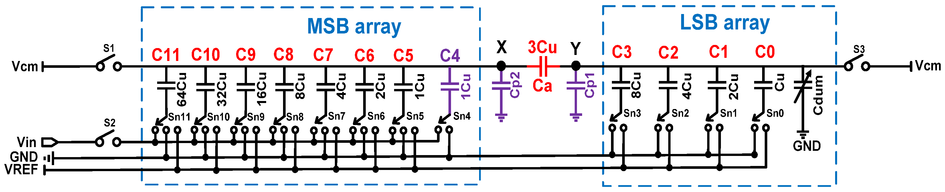
Figure 3.
The DAC capacitor array during the calibration. (a) Sampling Vref in the LSB array; (b) the charge distribution.
Figure 3.
The DAC capacitor array during the calibration. (a) Sampling Vref in the LSB array; (b) the charge distribution.

Figure 4.
The proposed differential calibration method. (a) Sampling phase; (b) charge distribution phase.
Figure 4.
The proposed differential calibration method. (a) Sampling phase; (b) charge distribution phase.
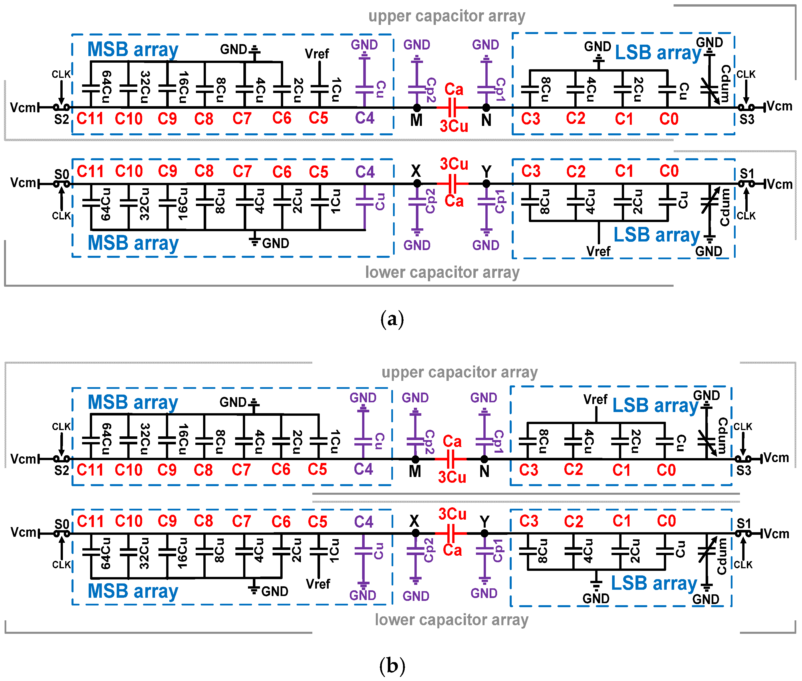
Figure 5.
The programmable capacitor Cdum.
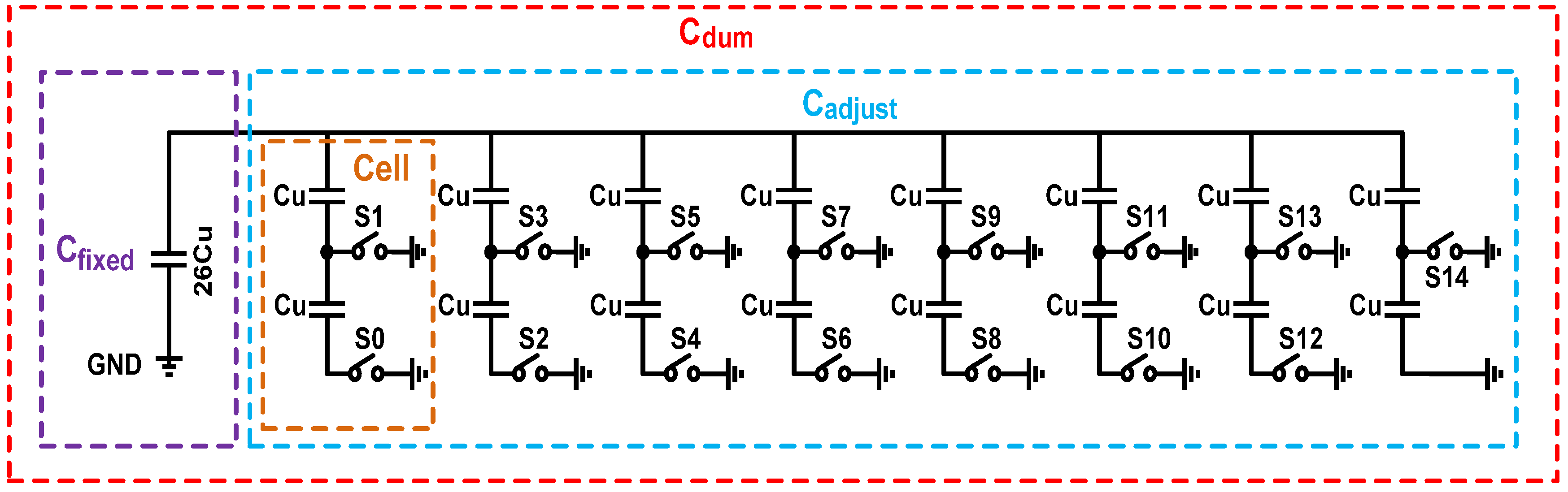
Figure 6.
The calibration circuit of the non-linearity.
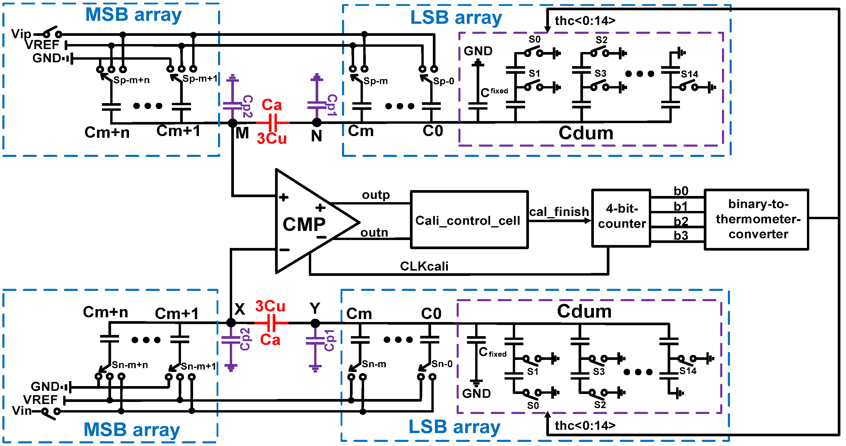
Figure 7.
Binary−scaled compensation. (a) Correction conversion; (b) conversion with a wrong decision.
Figure 7.
Binary−scaled compensation. (a) Correction conversion; (b) conversion with a wrong decision.

Figure 8.
Conventional bridge capacitor array.
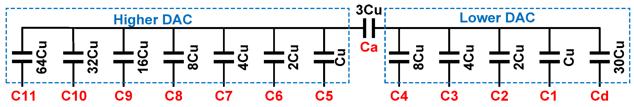
Figure 9.
Binary-scaled recombination method in the bridge structure.
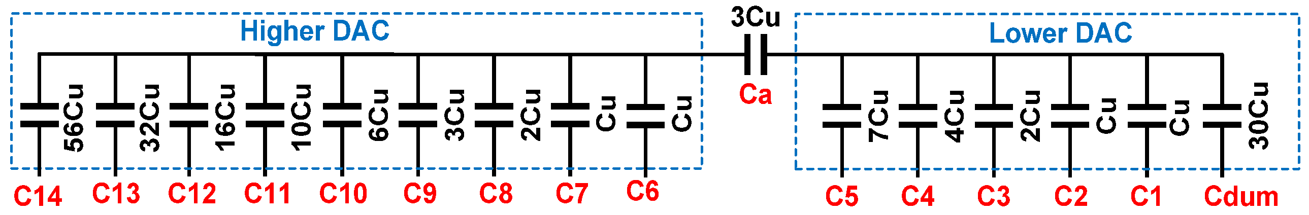
Figure 10.
Proposed hybrid redundancy based on the bridge capacitor array.

Figure 11.
Digital error correction logic.

Figure 12.
Bootstrapped switch.
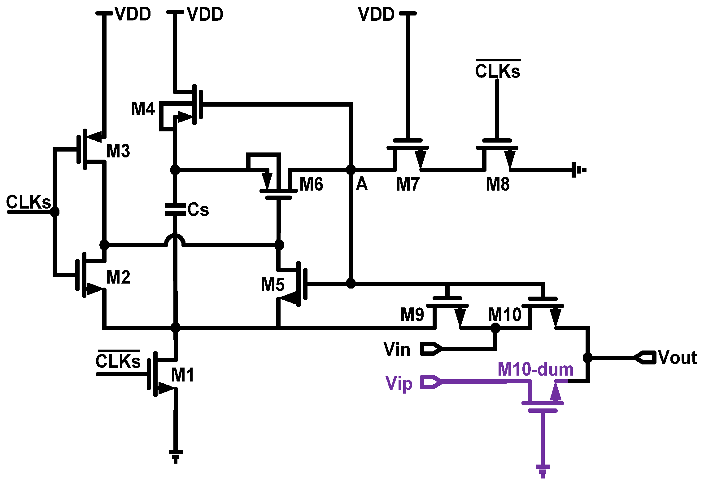
Figure 13.
Dynamic comparator.

Figure 14.
Asynchronous control logic.
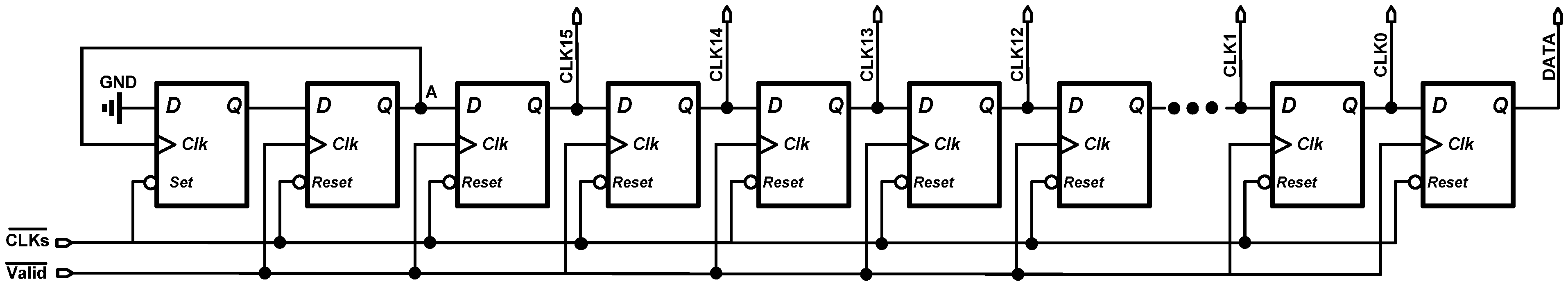
Figure 15.
Timing of the asynchronous control logic.

Figure 16.
DAC control logic.
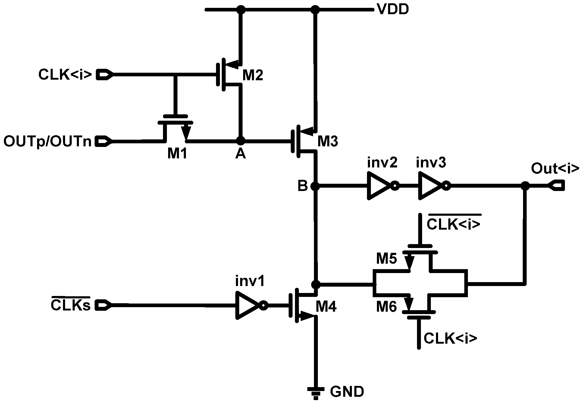
Figure 17.
DAC capacitor. (a) Unit capacitor structure; (b) floorplan of DAC capacitor array.

Figure 18.
The clock driver.

Figure 19.
Post simulation results of SNDR with temperature and corner.
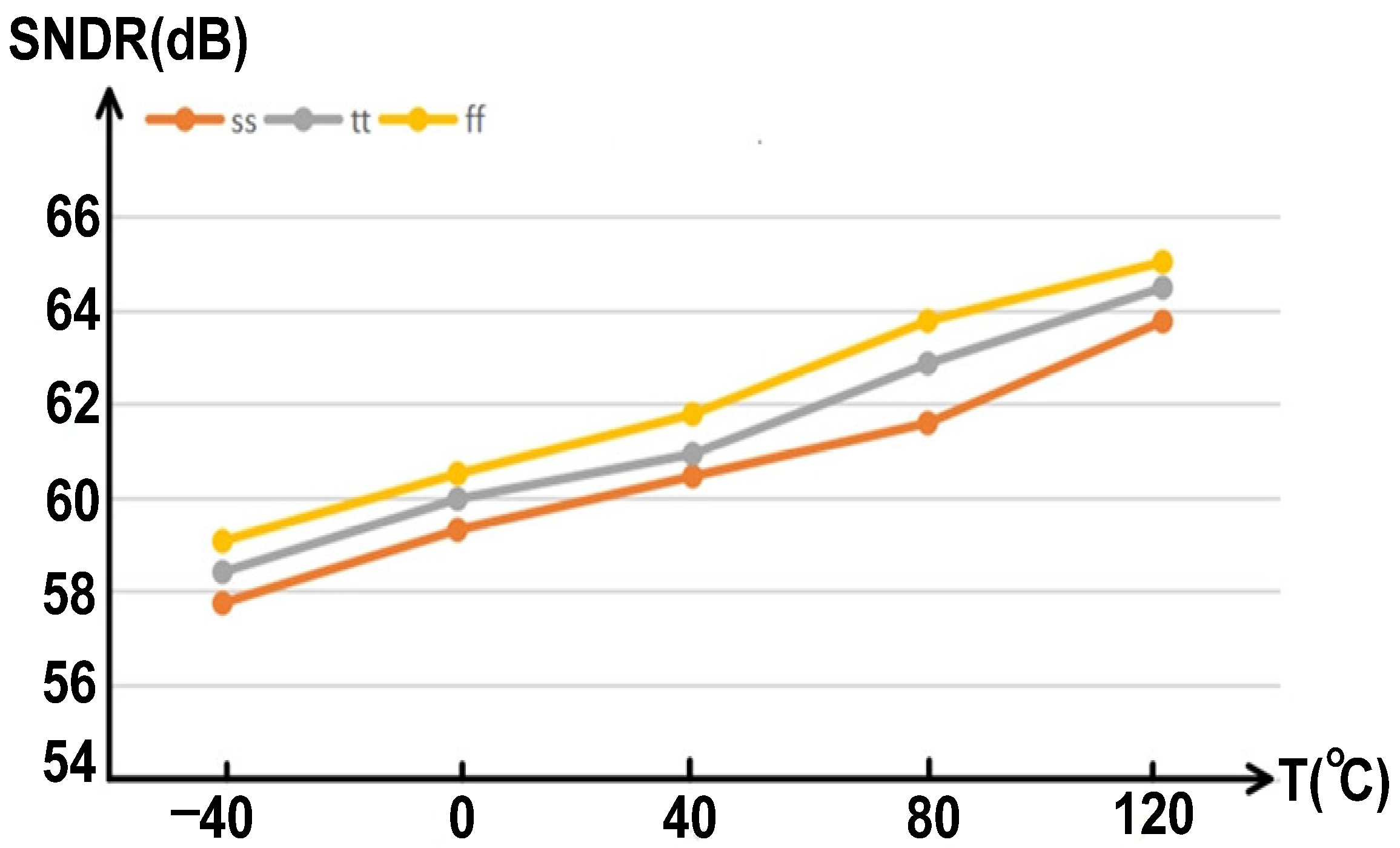
Figure 20.
Chip photograph and layout of the proposed SAR ADC.

Figure 21.
Measured Spectrum at Fin = 4.89 MHz when (a) calibration was off and (b) calibration was on.
Figure 21.
Measured Spectrum at Fin = 4.89 MHz when (a) calibration was off and (b) calibration was on.
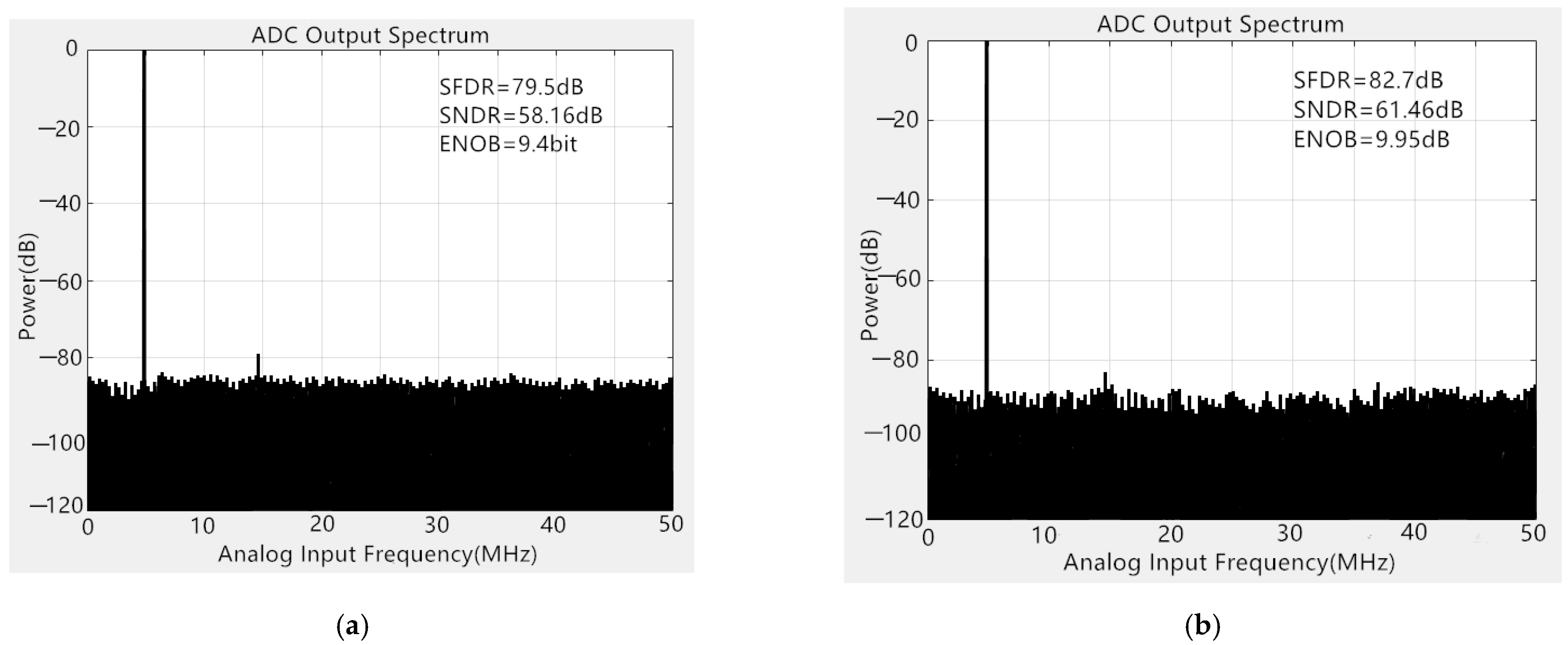
Figure 22.
Measured Spectrum at Fin = 49.96 MHz when (a) calibration was off and (b) calibration was on.
Figure 22.
Measured Spectrum at Fin = 49.96 MHz when (a) calibration was off and (b) calibration was on.

Figure 23.
Measured DNL (a) and INL (b) when the proposed calibration method was off.

Figure 24.
Measured DNL (a) and INL (b) when the proposed calibration method was on.

Table 1.
Comparison of redundant ranges with different redundant methods.
| Recombination [6] | Proposed Hybrid Method | |||
|---|---|---|---|---|
| 14 bit Cycles to Convert 13 bit | 16 bit Cycles to Convert 13 bit | |||
| Number of bit Cycling | bit Weighting | Redundancy Range (LSB) | bit Weighting | Redundancy Range (LSB) |
| 1 | 1792 | 512 | 1792 | 532 |
| 2 | 1024 | 256 | 1024 | 276 |
| 3 | 512 | 256 | 512 | 276 |
| 4 | 320 | 128 | 320 | 148 |
| 5 | 192 | 64 | 192 | 84 |
| 6 | 128 | 0 | 96 | 84 |
| 7 | 64 | 0 | 64 | 52 |
| 8 | 32 | 0 | 32 | 52 |
| 9 | 14 | 4 | 32 | 20 |
| 10 | 8 | 2 | 16 | 20 |
| 11 | 4 | 2 | 16 | 4 |
| 12 | 2 | 2 | 8 | 4 |
| 13 | 2 | 0 | 4 | 4 |
| 14 | 1 | 0 | 4 | 0 |
| 15 | 2 | 0 | ||
| 16 | 1 | 0 | ||
Table 2.
Performance summary and comparisions.
| This Work | [34] | [36] | [37] | [38] | [39] | ||
|---|---|---|---|---|---|---|---|
| Architecture | SAR | SAR | SAR | SAR | SAR | SAR | |
| CMOS technology | 28 nm | 20 nm | 65 nm | 40 nm | 40 nm | 14 | |
| Resolution (bits) | 12 | 10 | 11 | 12 | 12 | 12 | |
| Supply Voltage (V) | 0.9 | 1 | 1.2 | 1 | 0.9 | 0.8 | |
| Sampling Rates (MS/s) | 100 | 320 | 100 | 120 | 150 | 100 | |
| SNDR (dB) | @LF | 61.46 | 57.1 | 60 | 60.33 | 61.7 | 61.29 |
| @Nyquist | 58.82 | 50.9 | 58.8 | 58.1 | 56.2 | 58.34 | |
| SFDR (dB) | @LF | 82.7 | 78.1 | 74 | 72.9 | 74.4 | 82.08 |
| @Nyquist | 79.1 | 58.6 | 74.61 | 72 | 63.5 | 78.02 | |
| ENOB (bit) | @LF | 9.95 | 9.2 | 9.67 | 9.72 | 9.95 | 9.89 |
| @Nyquist | 9.51 | 8.16 | 9.51 | 9.35 | 9.0 | 9.40 | |
| Power (mW) | 0.86 | 1.52 | 1.6 | 1.9 | 1.5 | 0.78 | |
| FOM (fJ/conv-step) | @LF | 8.69 | 8.1 | 19.2 | 18.7 | 10.3 | 8.2 |
| @Nyquist | 11.8 | 16.5 | 21.9 | 24.26 | 18.5 | 11.15 | |
| Area (mm2) | 0.00227 | 0.0012 | 0.011 | 0.0128 | 0.04 | 0.112 | |
| DNL (LSB) | 0.754/−0.56 | 0.41/−0.34 | 1.05/−0.842 | 0.96/−0.93 | 1.77/−0.91 | — | |
| INL (LSB) | 0.83/−0.85 | 0.28/−0.43 | 1.28/−0.972 | 1.6/−1.08 | 2.95/−2.63 | — | |
Publisher’s Note: MDPI stays neutral with regard to jurisdictional claims in published maps and institutional affiliations. |
© 2022 by the authors. Licensee MDPI, Basel, Switzerland. This article is an open access article distributed under the terms and conditions of the Creative Commons Attribution (CC BY) license (https://creativecommons.org/licenses/by/4.0/).
Share and Cite
MDPI and ACS Style
Zheng, Y.; Ye, F.; Ren, J. A 12-Bit, 100 MS/s SAR ADC Based on a Bridge Capacitor Array with Redundancy and Non-Linearity Calibration in 28 nm CMOS. Electronics 2022, 11, 705. https://doi.org/10.3390/electronics11050705
AMA Style
Zheng Y, Ye F, Ren J. A 12-Bit, 100 MS/s SAR ADC Based on a Bridge Capacitor Array with Redundancy and Non-Linearity Calibration in 28 nm CMOS. Electronics. 2022; 11(5):705. https://doi.org/10.3390/electronics11050705
Chicago/Turabian StyleZheng, Yan, Fan Ye, and Junyan Ren. 2022. "A 12-Bit, 100 MS/s SAR ADC Based on a Bridge Capacitor Array with Redundancy and Non-Linearity Calibration in 28 nm CMOS" Electronics 11, no. 5: 705. https://doi.org/10.3390/electronics11050705
Note that from the first issue of 2016, this journal uses article numbers instead of page numbers. See further details here.