
A Simple Commutation Method and a Cost-Effective Clamping Circuit for Three-to-Five-Phase Indirect-Matrix Converters


1
Department of Electromechanical, Systems and Metal Engineering, Ghent University, 9000 Ghent, Belgium
2
FlandersMake@UGent—Corelab EEDT-MP, 3001 Leuven, Belgium
3
Department of Electrical Engineering, Faculty of Engineering, Menoufia University, Menoufia 32511, Egypt
4
Electrical Engineering Department, Kafrelshiekh University, Kafrelshiekh 33511, Egypt
*
Author to whom correspondence should be addressed.
Electronics 2022, 11(5), 808; https://doi.org/10.3390/electronics11050808
Submission received: 8 February 2022
/
Revised: 24 February 2022
/
Accepted: 2 March 2022
/
Published: 4 March 2022
(This article belongs to the Special Issue Power Electronic Converters in a Multiphase Drive Systems)
Abstract
:This article presents and analyzes a three-to-five-phase indirect matrix converter (IMC) structure for directly supplying a five-phase static load from a three-phase supply. The IMC topology offers a lower number of switches, a simple commutation procedure and a cost-effective clamping circuit in comparison to the direct matrix converter (DMC). A simple clamping circuit with one ultrafast diode and one small capacitor is proposed to protect the switches of the IMC from overvoltage. The issues of powering up the IMC with the simple clamping circuit is discussed in detail. The instructions for the safe start-up of the IMC with the proposed clamping circuit is introduced based on the simulated and the measured analyses. Moreover, a carrier-based pulse-width-modulation () method is also presented in order to control the switches of the IMC. The presented CBPWM method creates PWM pulses for both the inverter and the rectifier legs by using only one symmetric and triangular carrier signal. Finally, experimental and simulation testing with a five-phase R–L load demonstrate the viability and the efficiency of the introduced CBPWM algorithm for the suggested IMC.
1. Introduction
Multi-phase drive systems are vital in high-reliability applications where a better fault-tolerant property is a must to ensure operation under exceptional circumstances [1,2]. The combination of the high-power operating requirement and the robustness requirements are widely represented in aerospace applications and electric vehicles [2,3,4]. Multi-phase drive systems also offer characteristics that make them competitive in a variety of different industries. The number of phases in electric machines can be increased to improve torque-density, reduce noise and vibrations levels, and develop multi-motor technologies [5,6,7,8].
A multi-phase rectifier-inverter converter is generally used to energize a multi-phase motor drive. However, this converter entails a large reactive DC-link element, which is a specific scrawny point in a harsh environment [9]. This difficulty is eliminated using the matrix converter (MC) [10]. A direct AC-to-AC conversion of power without the need for DC-energy storage is possible with MCs. They have lately received a lot of attention as an alternative to the traditional rectifier inverter [11,12]. Many benefits can be obtained from MCs, including sinusoidal input- and output-current waveforms, high power density, unity-input-power factor and four-quadrant operation [13,14]. Furthermore, because of the nonexistence of the massive DC-link electrolytic capacitors for energy storage, MCs are very dependable and robust [15,16].
There are a number of other advantages to using MCs in a practical manner. First, thanks to the introduction of SiC and GaN technologies, this topology tends to solve the problem of thermal management, and it performs significantly better under high-temperature circumstances than traditional DC-link topologies [17,18]. Second, the switches in the MCs are exposed to lower voltage stress compared to the switches in traditional converters. Despite the increased number of IGBTs, the MCs’ success rates are improved by the lesser stress on their switches. As a result, these converters (MCs) have a better level of reliability than traditional converters (DC-link rectifier inverters) [16,17,18]. Manufacturers such as Yaskawa, Siemens, ABB, and others have expressed their interest in this converter for the reasons stated above. Consequently, there is a lot of work being done to use this technology in more electric and quieter aircrafts.
Direct (DMC) and indirect (IMC) MCs are the two different forms of MCs. The three-to-five-phase DMC is a one-stage AC-to-AC direct converter with 15 bidirectional switches that directly link the three-phase input voltages to the five-phase output loads as shown in Figure 1a [17,18]. Nevertheless, this topology necessitates a large number of power switches, multi-step-commutation techniques, and complex overvoltage-protection circuits. The IMC structure is built using an AC-to-DC-to-AC power conversion with no massive intermediary capacitor. The IMC is divided into two stages, the rectifier stage and the inverter stage, as reported in Figure 1b [19]. The maximum value of the voltage-transfer ratio and the characteristics of the input/output are all the same between the DMC and the IMC topologies. The IMC architecture, on the other hand, allows for soft-switching commutation, which is not possible in the DMC topology. In addition, as compared to the DMC, the IMC requires a simpler clamping circuit, which is utilized to avoid the IMC’s switches from breaking down due to overvoltage. Figure 1c shows the conventional clamping circuit for the three-to-five-phase MC, which consists of 16 ultrafast diodes, a clamping capacitor, and resistance. Moreover, the IMCs have the capability of reducing the number of power switches. The IMC has 22 IGBTs compared to 30 IGBTs in the case of the DMC, as described in Figure 1. In addition, the IMC has the capability of supplying the electricity to an imbalanced or nonlinear three-phase load. This is accomplished by placing an extra leg at the inverter stage. The voltage-transfer ratio in the case of the IMC can be increased by adding a Z-source network between the rectifier and the inverter stages [20,21]. In the IMC, the rectifier-stage switches are commutated at zero current, which minimizes the rectifier switching losses. Consequently, the rectifier stage achieves safer commutation and lower switching losses. The IMC has lately received a lot of attention, and several researchers have created numerous IMC topologies that are suited for certain applications. The authors of [22,23] focused on using zero-current commutation to enhance the structure of the rectifier stage in the IMC using reduced-power devices.
Besides the advancement of MC topologies, pulse-width-modulation (PWM) techniques have lately attracted a lot of attention [24,25]. The space-vector-PWM (SVPWM) and carrier-based-PWM (CBPWM) techniques are two PWM schemes for IMCs. Some parts of the SVPWM technique are complicated [16,21,26,27,28]. In recent years, researchers have used the CBPWM technique to simplify the SVPWM [14,29,30,31,32]. The carrier signal used in the rectifier stage of the conventional CBPWM method [29,30,31,32] differs from that used in the inverter stage; the rectifier-stage carrier signal is a symmetrical triangular signal, whereas the inverter-stage carrier signal is an asymmetrical triangular signal with different slopes of the rising and falling edges. Furthermore, because of the fluctuation in the DC-link voltage, the slopes of the asymmetrical carrier signal differ at each sampling interval. To overcome the drawbacks of the conventional CBPWM method, the authors of [33] proposed an effective alternative method that is suitable for the three-to-five-phase IMC topology by generating the PWM signals for all of the switches in both the rectifier and five-phase-inverter stages using only one symmetrical triangular carrier signal.
The majority of the scientific focus on the MC is dedicated to enhancing modulation (SVM [34], CBPWM [33], direct torque control [35], etc.), control techniques (wind generation [36], distributed generation [37], loss reduction [38], common mode voltage reduction [39], sensorless control [40], etc.), waveform quality [41], stability analysis [42], and semisoft commutation [43], etc. However, there are just a few publications that look into MC hardware and the issues that come with it. The majority of them focus on novel switches with reverse-blocking capability (reverse-blocking IGBT) [44] and clamp circuits [45] as MC-protection circuits. Most of the protection circuits use the conventional clamping circuit shown in Figure 1c. In [46], a simplified IMC structure with just six diodes in a clamp circuit is suggested, which has the same functionality as its twelve-diode version. In [47], an open-circuit analysis for a three-phase-to-three-phase IMC with a simple clamping circuit was proposed. The clamping circuit in [47] consists of only one diode and one capacitor. This clamping circuit is used with the introduced three-to-five-phase IMC. However, if several key considerations are not followed when working with the IMC, then this simple clamping circuit may cause damage to the matrix’s switches instead of protecting them. These key considerations are experimentally studied and discussed in this paper.
This paper introduces a three-to-five-phase indirect MC with a cost-effective and simple clamp circuit that consists of only one diode and one capacitor. A detailed discussion about the clamping circuit is introduced considering the issues concerned with charging the clamping capacitor and the start-up of the converter when the PWM of the rectifier is working. These issues are experimentally tested and analyzed. Moreover, a CBPWM based on space-vector modulation (SVM) is implemented. In this method, a zero-current commutation in the rectifier stage is maintained by using the CBPWM to minimize the switching losses. This is achieved by considering the synchronization between the rectifier and inverter stages, where the commutation in the rectifier stage occurs at the zero vectors of the inverter, i.e., at zero DC-link current. Hence, a lower switching loss is obtained. Finally, the simulated and the measured performances of the indirect MC with the CBPWM technique at different output frequencies are introduced and discussed.
2. Five-Phase Indirect-Matrix Converter
The proposed three-to-five-phase IMC’s power-circuit architecture is seen in Figure 1b. It comprises a rectifier stage and a five-phase inverter stage. Six bidirectional switches are used in the rectifier stage, whereas the inverter stage uses only ten unidirectional switches. The purpose of the rectifier stage is to build sinusoidal input currents while also keeping the DC-link voltage positive. The five-phase inverter stage produces five-phase output voltages with adjustable magnitude and frequency. The familiar theory of the indirect SVM is firstly introduced to describe the suggested IMC topology’s working principles.
2.1. Indirect Space Vector Modulation
The indirect SVM approach is a popular method to control the IMC. In this approach, there are two stages (the rectifier stage and the inverter stage). The required input current, available input voltages, and required output voltages are used to compute the controlling pulses for the switches of the rectifier stage and the inverter stage.
2.1.1. Current-Source Rectifier
The rectifier stage comprises bidirectional switches as seen in Figure 1b. Because of the lack of bidirectional switches on the market, the bidirectional switches in the rectifier stage are made up of two unidirectional common-emitter switches. The input voltage to the rectifier stage can be described by Equation (1). In Equation (1), represents the input-phase number, e.g., . In Equation (1), and represent the frequency and the peak of the phase input voltage, respectively. In Equation (1), is 0, 1 and 2.
There are only nine switching states allowed for these switches in order to prevent a virtual DC-connection open circuit. These switching states are six non-zero (active) vectors () and three zero vectors () as represented by the hexagon in Figure 2a. For both the zero and active vectors, the duty cycles are determined using the yellow-colored vectors in Figure 2a, as shown in Equations (2)–(4) [34].
where is the input-current-modulation index with a value between 0 and 1. In addition, indicates the measured angle starting from the positive X-axis to the rectifier’s input reference-current vector (.
The zero-vectors are ignored during the rectifier-stage modulation with the aim of obtaining the greatest DC-link voltage. As a result, the switching sequence simply comprises the two active vectors, , whose duty cycles are , respectively, and can be defined by Equations (5) and (6) [16]. The average DC-link voltage in the first sector can be calculated from Equation (7). The switching states and the duty cycles for the other sectors may be determined using the same method as reported in Table 1.
2.1.2. Five-Phase Voltage-Source Inverter
The switches of the inverter stage have 32 allowed switching states in order to prevent the short circuit of the virtual DC link and the open circuit of the load terminals. There are 30 active vectors () in these states and 2 zero vectors as shown in the decagon in Figure 2b. There are three groups for the active vectors: small vectors (0.2472), medium vectors (0.4) and large vectors (0.6472) [48]. As shown in Equation (8) and Figure 2b, the reference output voltage () is obtained using the adjacent vectors (). The duty cycles of these adjacent vectors are calculated using the yellow-colored vectors in Figure 2b as in Equations (9)–(11). In Equations (9) and (10), indicates the measured angle starting from the first vector in the associated sector to the reference-output-voltage vector, and is the output-voltage-modulation index for the inverter [48].
In this paper, large and medium vectors are only considered in order to obtain the reference output voltage so as to reduce the amount of switching occurrences. The large- and medium-voltage-vector duty cycles are determined based on their length relative to each other. This is clarified in Equations (12)–(15).
Notice that the times of the medium and the large vector are 38.2% and 61.8% of the overall active time, respectively. Accordingly, the value of the reference-output-voltage vector is limited to 0.5257 [34]. For further minimization of switching, the switching sequence is arranged as in Equation (16) [49,50]. Table 2 describes the switching vectors that minimize switching losses in various sectors. The switching state V11 (10000) in Table 2 indicates that the inverter switches S7, S10, S12, S14 and S16 are turned on, while switches S8, S9, S11, S13 and S15 are turned off. Figure 3 depicts the switching pattern for the upper switches of the five-phase VSI in the first sector. It should be noticed that only one of the upper switches’ states is changed between two adjacent switching states.
2.2. Carrier-Based Pulse Width Modulation
The previously introduced indirect-SVM study demonstrates that the SVM for the five-phase indirect MC may be implemented following a complicated procedure. In the rectifier and the inverter stages, the selection of the operative vectors is carried out independently. Various and complex equations are employed to compute the duty ratios of the effective vectors in the rectifier and in the inverter stages. The rectifier and inverter stages’ switching states are then synchronized to produce balanced output voltages and to ensure a zero-current commutation in the rectifier stage. The CBPWM technique was created to solve these issues by making it simple to produce gating pulses for the rectifier and the inverter. PWM signals are generated in the CBPWM technique when the modulation signals are compared to a carrier signal with a high frequency (1/Ts). Accordingly, the method begins with identifying the carrier signal and the modulation signals. For both the rectifier and inverter stages in this study, just one symmetrical and triangular carrier signal is employed to produce PWM signals.
As illustrated in Figure 4 (a), the carrier signal () is defined as follows:
2.2.1. Current-Source Rectifier
For the rectifier and when the vector of the reference input current is located in the first sector, the switching pattern and the timing of the modulated switches can be described as shown in Figure 4 (b). The duration of the gate pulse of the switch S4 (T4) is defined by Equation (18). The modulated signal of the rectifier switch S4 ( is given by Equation (19). The operating pulse of switch S4 is obtained by comparing the modulated signal in Equation (19) with the carrier signal as seen in Figure 4 (b). The operating pulse of switch S6 is the complement of the pulse of switch S4, and switch S1 is constantly on in the first sector. Switches S2, S3 and S5 are constantly off in the first sector. The switching states and the duty cycles for other sectors may be determined using the same method as reported in Table 1.
2.2.2. Five-Phase Inverter
For the inverter, two modulation signals are provided in order to obtain the required output voltage despite the DC-link-voltage volatility. These signals are generated from duty ratios and , respectively. These duty ratios are dependent on the DC-link voltage as given by Equations (20) and (21). For example, two modulation signals and are required to create the gate signal for the top switch of phase . Figure 4 (a) depicts the waveforms of and , as well as the carrier signal (). Then, two pulses and are achieved by individually comparing the two modulation signals and with the carrier signal (). Finally, the logic-XNOR function is used to determine the gate signal for switch ( in Figure 1b), as illustrated in Figure 4 (c) and Equation (23). This is also clearly depicted in the block diagram illustrated in Figure 5. It can be clearly noticed from Figure 4 that when commutation occurs in the rectifier stage, the inverter stage works on the zero vectors to ensure the rectifier’s zero-DC-link-current commutation. As a result, during commutation, all currents flowing through the switches of the rectifier are zero. The rectifier stage’s switching loss is reduced, and a complicated multi-step-commutation procedure is avoided.
For a generic formulation for the other phases, the modulation signals for switch can be written as in Equations (24) and (25). In Equations (24)–(27), M represents the output phase number A, B, C, D and E, and indicate the maximum and minimum values of the output phase voltages, respectively.
3. Clamping Circuit and Input Filter
This section introduces the input filter and the simple clamping circuit that are used with the three-to-five-phase indirect MC. The start-up issues and difficulties associated with the proposed clamping circuit are investigated in this section. The experimental validation for these issues is also presented in this section. The guidelines for the safe start-up of the proposed IMC with the simple clamping circuit is introduced.
3.1. Analysis of Clamping Circuit
The lack of the DC connection, which is common in other voltage-source-inverter topologies, is one of the most appealing features of the MC design when used in aviation applications. As a result, with an MC, no electrolytic capacitors are needed. Therefore, the removal of the load’s energy in some situations, such as an over-current situation, a failure in the commutation process, and/or during start-up of the operation of the MC, might cause overvoltage at the converter’s input because the matrix converter does not have an energy-storage facility. A diode bridge with ultrafast diodes linked to each input and output side of the MC, as well as a capacitor, is definitely the most commonly employed protection approach [51]. However, this two-bridge clamping circuit can be easily replaced by the simple clamping circuit shown in Figure 1b. It consists of only one diode and one capacitor.
The capacitor must store all of the inductive load energy without causing harmful overvoltages; therefore, it must be properly sized. The capacitor size is determined using the maximum stored load energy () in motor inductance (L) and the maximum accessible clamp voltage, and may be computed as follows:
The change in the clamp-capacitor stored energy from its starting voltage to its final voltage may be utilized to compute the capacitor size, as illustrated in Equation (29). In Equation (29), Cc represents the capacitance of the clamping capacitor, represents the maximum voltage allowable for MC switches and VMIN represents the initial voltage of the capacitor.
For high-power multi-phase drives, e.g., with 17.3 A (peak current), 0.05 H inductance, and 1200 V as the maximum allowable voltage for switches [2], the clamping circuit is chosen as 110 μF as a safety. When supplying these high-power drive systems with the proposed three-to-five-phase indirect MC (given in Figure 1b) with the proposed clamped circuit with a capacitor of 110 μF, there are some issues related to powering up the MC, e.g., due to inrush current and start-up with the operation of the PWM of the rectifier. To clarify these issues and determine their impact, simulation and experimental results have already been generated for the proposed indirect MC.
Figure 6 displays the simulation results for testing of the clamping circuit at start-up with the operation of the PWM of the rectifier. It can be noticed from Figure 6b that there is an extremely high supply current while charging the capacitor up to about 600 A, which causes current protection to work and a sudden trip of the circuit breaker occurs, and as a result an extremely high voltage occurs that causes the breakdown of matrix switches. Hence, the rectifier PWM must be stopped during the start-up of the MC.
Figure 7 describes the simulation results for the testing of the clamping circuit at start-up without operation of the PWM of the rectifier, and with the capacitor being charged using any line voltage, e.g., Vab. It can be noticed from Figure 7c that the maximum input current during capacitor charging is about 15 A. However, there is a high pulse current at time zero. This is because the start-up is not at zero voltage, as shown in Figure 7a.
Figure 8 shows the simulation results for the testing of the clamping circuit at start-up without operating the PWM of the rectifier and with the capacitor being charged using any line voltage at the instant of zero crossing. The maximum supply current in this case is about 10 A.
Figure 9 shows the experimental results of testing the clamping circuit at start-up without operating the PWM of the rectifier and charging using the ramp-line voltage Vab. Figure 10 describes the experimental results of testing the clamping circuit at start-up without operating the PWM of the rectifier and charging using the step-input-line voltage Vab. Hence, it is concluded from these figures that the start-up of the proposed MC should consider the following conditions: (1) the PWM of the rectifier stage should be held during the start-up until the capacitor charging finishes and (2) the capacitor charging should be done using any line voltage and this input-line voltage must be smoothly increased from zero up to the operating value.
3.2. Low-Pass Input Filter
The inductive impact of the power grid should be decreased since MC functions as a current-source-inverter on the input side and a voltage-source-inverter on the output side. A low-pass input filter is used to remove the high-frequency ripple from the waveform of the input current to the IMC. Figure 11 shows the input-filter structure [51]. In Figure 11, Rf, Cf and Lf represent damping resistance, filter capacitance and filter inductance, respectively.
4. Results and Discussion
This section introduces and analyzes the performance of the indirect MC for both the experimental and simulation results. The three-to-five-phase indirect MC is supplied from a three-phase AC supply of 50 Hz and 100 V peak value. The five-phase output terminals of the indirect MC are connected to a static five-phase R–L load ( = 82 Ω and = 10 mH). An input filter is connected between the supply and the input terminals of the indirect MC. The input-filter parameters are the following: = 3 mH, Rf = 50 Ω and =10 μF. The clamping circuit consists of a 110 μF capacitor and one ultrafast diode MUR860. The CBPWM is applied in order to control the indirect MC with minimal switching losses in the rectifier stage. The switching frequency is 10 kHz. The sampling times at the simulation and experimental measurements are 1 μs and 100 μs, respectively. The voltage-transfer ratio is chosen as 0.78.
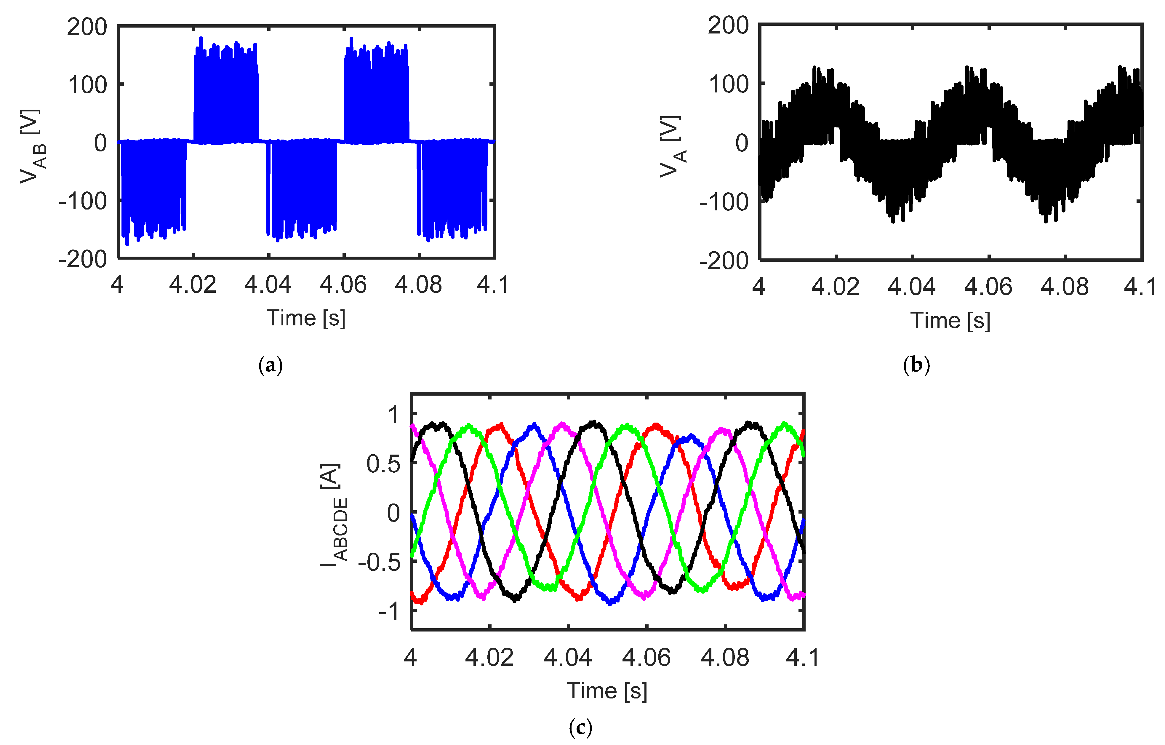
Figure 12 shows the test bench used in the experimental measurements. The MC is controlled to give different output frequencies, e.g., 100 Hz, 50 Hz and 25 Hz. Figure 13 and Figure 14 show the simulation and the experimental results for the MC at 50 Hz of output frequency, respectively. The simulation and experimental results of the DC-link voltage are shown in Figure 13a and Figure 15b, respectively. The input voltage to the MC during the experimental measurements is shown in Figure 15a. There is a great agreement between the measured and the simulated results. Figure 16 and Figure 17 show the simulation and the experimental results for the MC at 100 Hz of output frequency, respectively. Figure 18 and Figure 19 display the simulation and the experimental results for the MC at 25 Hz of output frequency, respectively.
5. Conclusions
In this article, a three-to-five-phase indirect-matrix converter (IMC) with a simple clamp circuit was presented. The suggested converter has the same properties as the three-to-five direct-matrix converter (DMC), despite the fact that the number of semiconductors (IGBTs) was decreased and the commutation procedure was simplified. The IMC has 22 IGBTs compared to 30 IGBTs in the case of the DMC. In addition, a simple clamping circuit with one ultrafast diode and one capacitor was used to protect the switches from overvoltage. A detailed discussion of the issues related to powering up the MC was introduced. Experimental and simulation tests, which had already been performed in order to show these issues and their solutions, was suggested. Moreover, a CBPWM technique appropriate for the introduced three-to-five-phase IMC structure was introduced. The introduced CBPWM technique generates the required PWM pulses for both the rectifier- and inverter-stage controllers using just one symmetrical and triangular carrier signal. Finally, experimental testing with a five-phase static R–L load demonstrated the viability of the implemented CBPWM algorithm for the suggested indirect MC.
Author Contributions
Conceptualization, K.B.T.; methodology, K.B.T.; software, K.B.T.; validation, K.B.T.; investigation, K.B.T.; writing—original draft preparation, K.B.T.; writing—review and editing, M.N.I., P.S.; visualization, M.N.I., P.S.; supervision, M.N.I., P.S. All authors have read and agreed to the published version of the manuscript.
Funding
The authors acknowledge the Special Research Fund of Ghent University (BOF.DCV.2019.0011.01).
Conflicts of Interest
The authors declare no conflict of interest.
References
- Vancini, L.; Mengoni, M.; Rizzoli, G.; Sala, G.; Zarri, L.; Tani, A. Carrier-Based PWM Overmodulation Strategies for Five-Phase Inverters. IEEE Trans. Power Electron. 2021, 36, 6988–6999. [Google Scholar] [CrossRef]
- Tawfiq, K.B.; Ibrahim, M.N.; El-Kholy, E.E.; Sergeant, P. Construction of Synchronous Reluctance Machines with Combined Star-Pentagon Configuration Using Standard Three-Phase Stator Frames. IEEE Trans. Ind. Electron. 2021. [Google Scholar] [CrossRef]
- Wang, K.; Gu, Z.Y.; Liu, C.; Zhu, Z.Q. Design and Analysis of a Five-Phase SPM Machine Considering Third Harmonic Current Injection. IEEE Trans. Energy Convers. 2018, 33, 1108–1117. [Google Scholar] [CrossRef]
- Tawfiq, K.B.; Ibrahim, M.N.; El-Kholy, E.E.; Sergeant, P. Comparative Analysis of Refurbishing Methods of Three-phase Synchronous Reluctance Machines to Five-phase with Minimum Cost. IEEE Trans. Ind. Appl. 2021, 57, 6007–6022. [Google Scholar] [CrossRef]
- Kong, W.; Kang, M.; Li, D.; Qu, R.; Jiang, D.; Gan, C. Investigation of spatial harmonic magnetic field coupling effect on torque ripple for multiphase induction motor under open fault condition. IEEE Trans. Power Electron. 2017, 33, 6060–6071. [Google Scholar] [CrossRef]
- Levi, E.; Jones, M.; Vukosavic, S.N.; Toliyat, H.A. A novel concept of a multiphase, multimotor vector-controlled drive system supplied from a single voltage source inverter. IEEE Trans. Power Electron. 2004, 19, 320–335. [Google Scholar] [CrossRef]
- Li, L.; Lee, K.; Bai, K.; Ouyang, X.; Yang, H. Inverse models and harmonics compensation for suppressing torque ripples of multiphase permanent magnet motor. IEEE Trans. Ind. Electron. 2018, 65, 8730–8739. [Google Scholar] [CrossRef]
- Mengoni, M.; Zarri, L.; Tani, A.; Parsa, L.; Serra, G.; Casadei, D. High torque-density control of multiphase induction motor drives operating over a wide speed range. IEEE Trans. Ind. Electron. 2015, 62, 814–825. [Google Scholar] [CrossRef]
- Kolar, J.W.; Friedli, T.; Rodriguez, J.; Wheeler, P.W. Review of three phase PWM AC–AC converter topologies. IEEE Trans. Ind. Electron. 2011, 58, 4988–5006. [Google Scholar] [CrossRef]
- Tran, Q.; Lee, H. A Three-Vector Modulation Strategy for Indirect Matrix Converter Fed Open-End Load to Reduce Common-Mode Voltage with Improved Output Performance. IEEE Trans. Power Electron. 2017, 32, 7904–7915. [Google Scholar] [CrossRef]
- Nguyen, T.D.; Lee, H. Development of a Three-to-Five-Phase Indirect Matrix Converter with Carrier-Based PWM Based on Space-Vector Modulation Analysis. IEEE Trans. Ind. Electron. 2016, 63, 13–24. [Google Scholar] [CrossRef]
- Tran, Q.; Lee, H. An Advanced Modulation Strategy for Three-to-Five-Phase Indirect Matrix Converters to Reduce Common-Mode Voltage with Enhanced Output Performance. IEEE Trans. Ind. Electron. 2018, 65, 5282–5291. [Google Scholar] [CrossRef]
- Nguyen, T.D.; Lee, H. A New SVM Method for an Indirect Matrix Converter with Common-Mode Voltage Reduction. IEEE Trans. Ind. Inform. 2014, 10, 61–72. [Google Scholar] [CrossRef]
- Nguyen, T.D.; Lee, H. Dual Three-Phase Indirect Matrix Converter with Carrier-Based PWM Method. IEEE Trans. Power Electron. 2014, 29, 569–581. [Google Scholar] [CrossRef]
- Tran, Q.H.; Nguyen, T.D.; Phuong, L.M. Simplified Space-Vector Modulation Strategy for Indirect Matrix Converter with Common-Mode Voltage and Harmonic Distortion Reduction. IEEE Access 2020, 8, 218489–218498. [Google Scholar] [CrossRef]
- Kolar, J.W.; Schafmeister, F.; Round, S.D.; Ertl, H. Novel three-phase AC–AC sparse matrix converters. IEEE Trans. Power Electron. 2007, 22, 1649–1661. [Google Scholar] [CrossRef]
- Wang, B.; Sherif, E. Spectral analysis of matrix converters based on 3-D fourier integral. IEEE Trans. Power Electron. 2013, 28, 19–25. [Google Scholar] [CrossRef]
- Rivera, M.; Rojas, C.; Rodríguez, J.; Wheeler, P.; Wu, B.; Espinoza, J.R. Predictive current control with input filter resonance mitigation for a direct matrix converter. IEEE Trans. Power Electron. 2011, 26, 2794–2803. [Google Scholar] [CrossRef]
- Jayaprakasan, S.; Ashok, S.; Ramchand, R. Analysis of Current Error Space Phasor for a Space Vector Modulated Indirect Matrix Converter. IEEE Trans. Ind. Electron. 2022, 69, 4451–4459. [Google Scholar] [CrossRef]
- Liu, X.; Loh, P.C.; Wang, P.; Han, X. Improved modulation schemes for indirect Z-source matrix converter with sinusoidal input and output waveforms. IEEE Trans. Power Electron. 2012, 27, 4039–4050. [Google Scholar] [CrossRef]
- Park, K.; Lee, K.-B.; Blaabjerg, F. Improving output performance of a Z-source sparse matrix converter under unbalanced input-voltage conditions. IEEE Trans. Power Electron. 2012, 27, 2043–2054. [Google Scholar] [CrossRef]
- Friedli, T.; Round, S.D.; Kolar, J.W. A 100 kHz SiC sparse matrix converter. In Proceedings of the IEEE Power Electronics Specialists Conference, Orlando, FL, USA, 17–21 June 2007; IEEE: New York, NY, USA, 2007; pp. 2148–2154. [Google Scholar]
- Schonberger, J.; Friedli, T.; Round, S.D.; Kolar, J.W. An ultra-sparse matrix converter with a novel active clamp circuit. In Proceedings of the Power Conversion Conference-Nagoya, Nagoya, Japan, 2–5 April 2007; IEEE: New York, NY, USA, 2007; pp. 784–791. [Google Scholar]
- Sun, Y. Indirect matrix converter-based topology and modulation schemes for enhancing input reactive power capability. IEEE Trans. Power Electron. 2015, 30, 4669–4681. [Google Scholar] [CrossRef]
- Espina, J. Reduction of output common mode voltage using a novel SVM implementation in matrix converters for improved motor lifetime. IEEE Trans. Ind. Electron. 2014, 61, 5903–5911. [Google Scholar] [CrossRef] [Green Version]
- Wei, L.; Lipo, T.L. A novel matrix converter topology with simple commutation. In Proceedings of the 36th IAS Annual Meeting, Chicago, IL, USA, 30 September–4 October 2001; IEEE: New York, NY, USA, 2001; pp. 1749–1754. [Google Scholar]
- Garcia, C. A simple current control strategy for a four-leg indirect matrix converter. IEEE Trans. Power Electron. 2015, 30, 2275–2287. [Google Scholar] [CrossRef]
- Cárdenas, R.; Juri, C.; Peña, R.; Wheeler, P.; Clare, J. The application of resonant controllers to four-leg matrix converters feeding unbalanced or nonlinear loads. IEEE Trans. Power Electron. 2012, 27, 1120–1129. [Google Scholar] [CrossRef]
- Loh, P.C.; Rong, R.; Blaabjerg, F.; Wang, P. Digital carrier modulation and sampling issues of matrix converters. IEEE Trans. Power Electron. 2009, 24, 1690–1700. [Google Scholar] [CrossRef]
- Chiang, G.T.; Itoh, J. Comparison of two overmodulation strategies in an indirect matrix converter. IEEE Trans. Ind. Electron. 2013, 60, 43–53. [Google Scholar] [CrossRef]
- Wang, B.; Venkataramanan, G. A carrier-based PWM algorithm for indirect matrix converters. In Proceedings of the 37th IEEE Power Electronics Specialists Conference, Jeju, Korea, 18–22 June 2006; IEEE: New York, NY, USA, 2006; pp. 1–8. [Google Scholar]
- Baranwal, R.; Basu, K.; Mohan, N. Carrier-based implementation of SVPWM for dual two-level VSI and dual matrix converter with zero common-mode voltage. IEEE Trans. Power Electron. 2015, 30, 1471–1487. [Google Scholar] [CrossRef]
- Nguyen, T.D.; Lee, H.-H. Carrier-based PWM technique for three-to five phase indirect matrix converters. In Proceedings of the IECON 2011—37th Annual Conference of the IEEE Industrial Electronics Society, Melbourne, VIC, Australia, 7–10 November 2011; IEEE: New York, NY, USA, 2011; pp. 3662–3667. [Google Scholar]
- Tawfiq, K.B.; Ibrahim, M.N.; El-Kholy, E.E.; Sergeant, P. An Enhanced Fault-Tolerant Control of a Five-Phase Synchronous Reluctance Motor Fed from a Three-to-Five-phase Matrix Converter. IEEE J. Emerg. Sel. Top. Power Electron. 2022. [Google Scholar] [CrossRef]
- Lee, K.B.; Blaabjerg, F. An improved DTC SVM method for sensorless matrix converter drives using an overmodulation strategy and a simple nonlinearity compensation. IEEE Trans. Ind. Electron. 2007, 54, 3155–3166. [Google Scholar] [CrossRef]
- Rebsdorf, A.; Helle, L. Variable Speed Wind Turbine Having a Matrix Converter. U.S. Patent 6,856,038, 20 May 2003. [Google Scholar]
- Nikkhajoei, H.; Iravani, M.R. A matrix converter based micro-turbine distributed generation system. IEEE Trans. Power Del. 2005, 20, 2182–2192. [Google Scholar] [CrossRef]
- Kwak, S. Indirect matrix converter drives for unity displacement factor and minimum switching losses. Electr. Power Syst. Res. 2007, 77, 447–454. [Google Scholar] [CrossRef]
- Cha, H.J.; Enjeti, P. An approach to reduce common-mode voltage in matrix converter. IEEE Trans. Ind. Appl. 2003, 39, 1151–1159. [Google Scholar]
- Lee, K.B.; Blaabjerg, F. Sensorless DTC-SVM for induction motor driven by a matrix converter using a parameter estimation strategy. IEEE Trans. Ind. Electron. 2008, 55, 512–521. [Google Scholar] [CrossRef]
- Arias, A.; Empringham, L.; Asher, G.; Wheeler, P.W.; Bland, P.M.; Apap, M.; Sumner, M.; Clare, J. Elimination of waveform distortions in matrix converters using a new dual compensation method. IEEE Trans. Ind. Electron. 2007, 54, 2079–2087. [Google Scholar] [CrossRef]
- Casadei, D.; Clare, J.; Empringham, L.; Serra, G.; Tani, A.; Trentin, A.; Wheeler, P.; Zarri, L. Large-signal model for the stability analysis of matrix converters. IEEE Trans. Ind. Electron. 2007, 54, 939–950. [Google Scholar] [CrossRef]
- Wheeler, P.; Rodriguez, J.; Clare, J.; Empringham, L.; Weinstein, A. Matrix converters: A technology review. IEEE Trans. Ind. Electron. 2002, 49, 276–288. [Google Scholar] [CrossRef]
- Klumpner, C.; Blaabjerg, F. Using reverse-blocking IGBTs in power converters for adjustable-speed drives. IEEE Trans. Ind. Appl. 2006, 42, 807–816. [Google Scholar] [CrossRef]
- Empringham, L.; de Lillo, L.; Wheeler, P.; Clare, J. Matrix converter protection for more electric aircraft applications. In Proceedings of the IECON 2006—32nd Annual Conference on IEEE Industrial Electronics, Paris, France, 6–10 November 2006; IEEE: New York, NY, USA, 2006; pp. 2564–2568. [Google Scholar]
- Klumpner, C. An indirect matrix converter with a cost-effective protection and control. In Proceedings of the 2005 European Conference on Power Electronics and Applications, Dresden, Germany, 11–14 September 2005; IEEE: New York, NY, USA, 2005. [Google Scholar]
- Shi, B.; Zhou, B. Open-circuit behavior analysis for indirect matrix converter. In Proceedings of the IECON 2017—43rd Annual Conference of the IEEE Industrial Electronics Society, Beijing, China, 29 October–1 November 2017; IEEE: New York, NY, USA, 2017; pp. 7338–7342. [Google Scholar]
- Tawfiq, K.B.; Ibrahim, M.N.; El-Kholy, E.E.; Sergeant, P. Performance Analysis of a Five-phase Synchronous Reluctance Motor Connected to Matrix Converter. In Proceedings of the 2021 IEEE International Electric Machines & Drives Conference (IEMDC), Hartford, CT, USA, 17–20 May 2021; IEEE: New York, NY, USA, 2021; pp. 1–6. [Google Scholar] [CrossRef]
- Nasir, U.; Costabeber, A.; Wheeler, P.; Rivera, M.; Clare, J. A Three-Phase Modular Isolated Matrix Converter. IEEE Trans. Power Electron. 2019, 34, 11760–11773. [Google Scholar] [CrossRef]
- Tawfiq, K.B.; Ibrahim, M.N.; Rezk, H.; El-Kholy, E.E.; Sergeant, P. Mathematical Modelling, Analysis and Control of a Three to Five-Phase Matrix Converter for Minimal Switching Losses. Mathematics 2021, 9, 96. [Google Scholar] [CrossRef]
- Nielsen, P.; Blaabjerg, F.; Pederson, J.K. Novel Solutions for Protection of Matrix Converter to Three Phase Induction Machine. In Proceedings of the IEEE IAS Conference Record, New Orleans, LA, USA, 5–9 October 1997; IEEE: New York, NY, USA, 1997; pp. 1447–1454. [Google Scholar]
Figure 1.
(a) DMC, (b) IMC and (c) conventional clamping circuit.

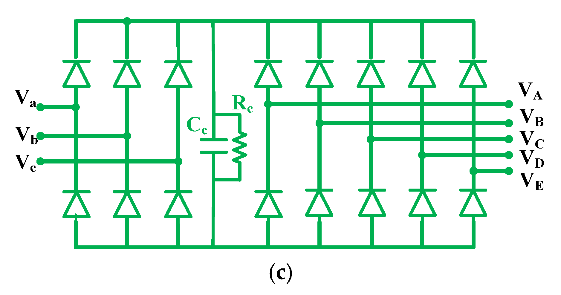
Figure 2.
(a) The rectifier’s hexagon and (b) the inverter’s decagon.
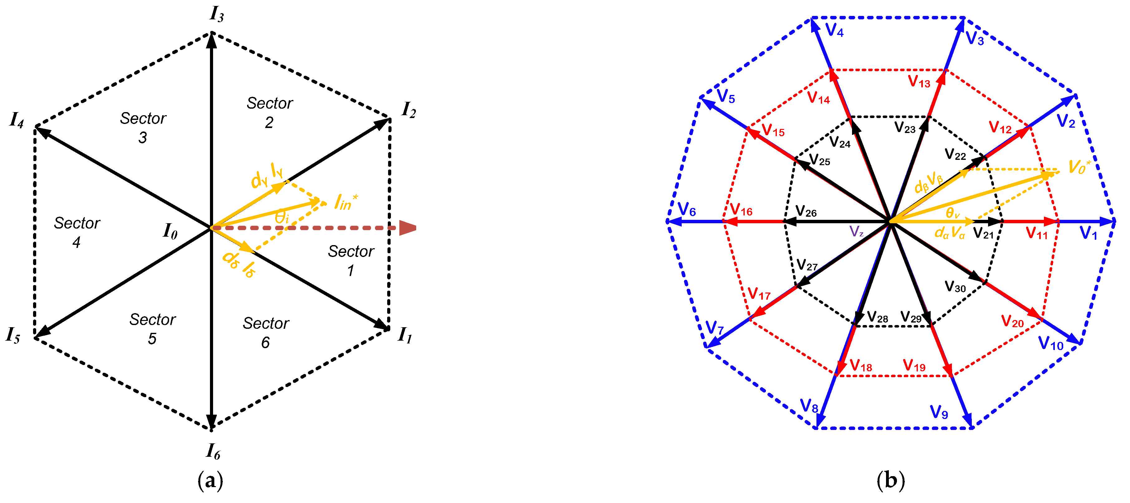
Figure 3.
Switching sequence for a five-phase voltage-source inverter (VSI) in the first sector.
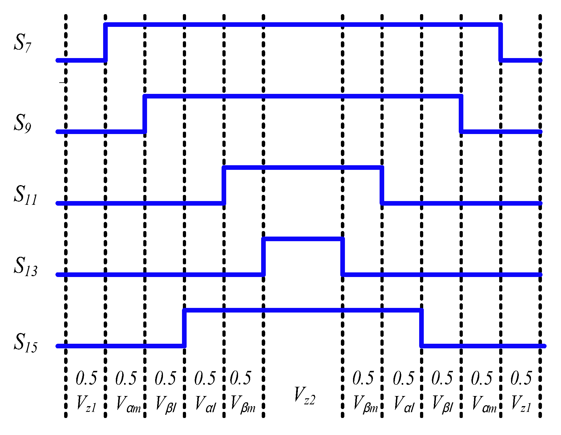
Figure 4.
(a) Carrier and modulation signals, (b) the duty cycle of rectifier and (c) inverter in sector 1 using CBPWM.
Figure 4.
(a) Carrier and modulation signals, (b) the duty cycle of rectifier and (c) inverter in sector 1 using CBPWM.
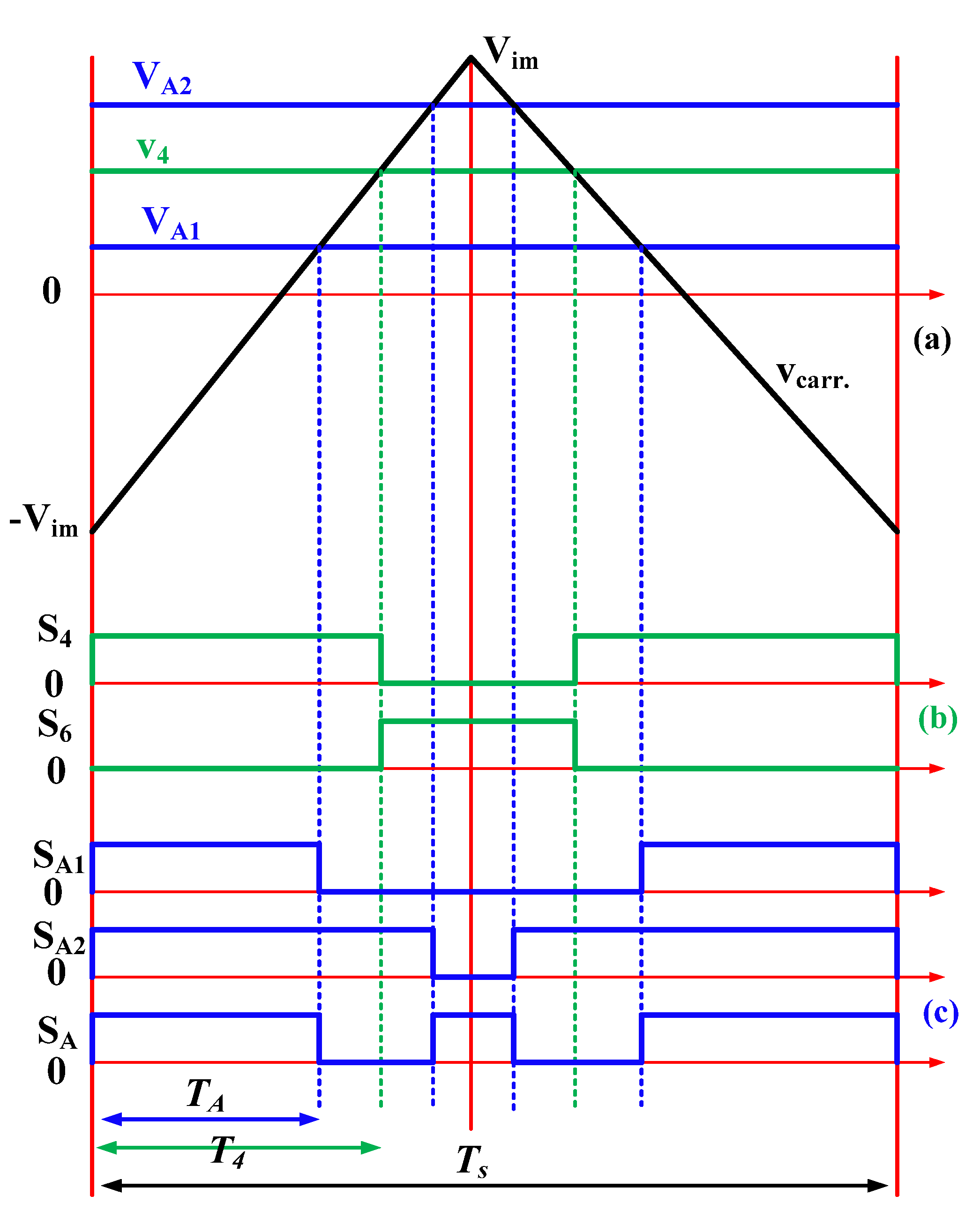
Figure 5.
The CBPWM block diagram for the inverter stage in the IMC.

Figure 6.
Simulation testing of the clamping circuit at start-up with operation of the PWM of the rectifier (a) DC-link voltage and (b) input current for MC.
Figure 6.
Simulation testing of the clamping circuit at start-up with operation of the PWM of the rectifier (a) DC-link voltage and (b) input current for MC.

Figure 7.
Simulation testing of the clamping circuit at start-up without operating the PWM of the rectifier and charging using line voltage Vab (a) Line-input voltage Vab, (b) DC-link voltage and (c) input current for MC.
Figure 7.
Simulation testing of the clamping circuit at start-up without operating the PWM of the rectifier and charging using line voltage Vab (a) Line-input voltage Vab, (b) DC-link voltage and (c) input current for MC.
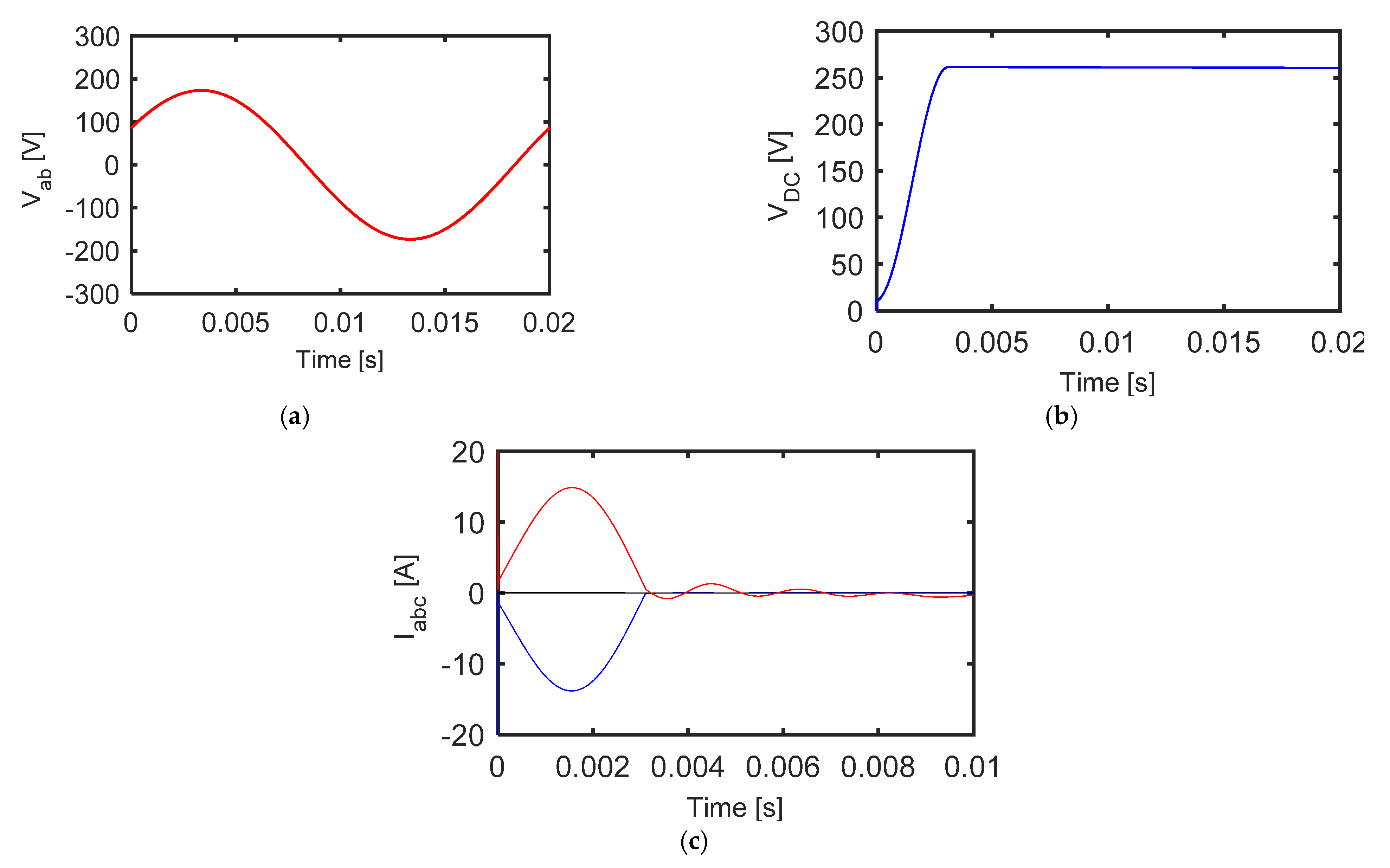
Figure 8.
Simulation testing of the clamping circuit at start-up without operating the PWM of the rectifier and charging using line voltage Vab at zero crossing (a) Line-input voltage Vab, (b) DC-link voltage and (c) input current for MC.
Figure 8.
Simulation testing of the clamping circuit at start-up without operating the PWM of the rectifier and charging using line voltage Vab at zero crossing (a) Line-input voltage Vab, (b) DC-link voltage and (c) input current for MC.
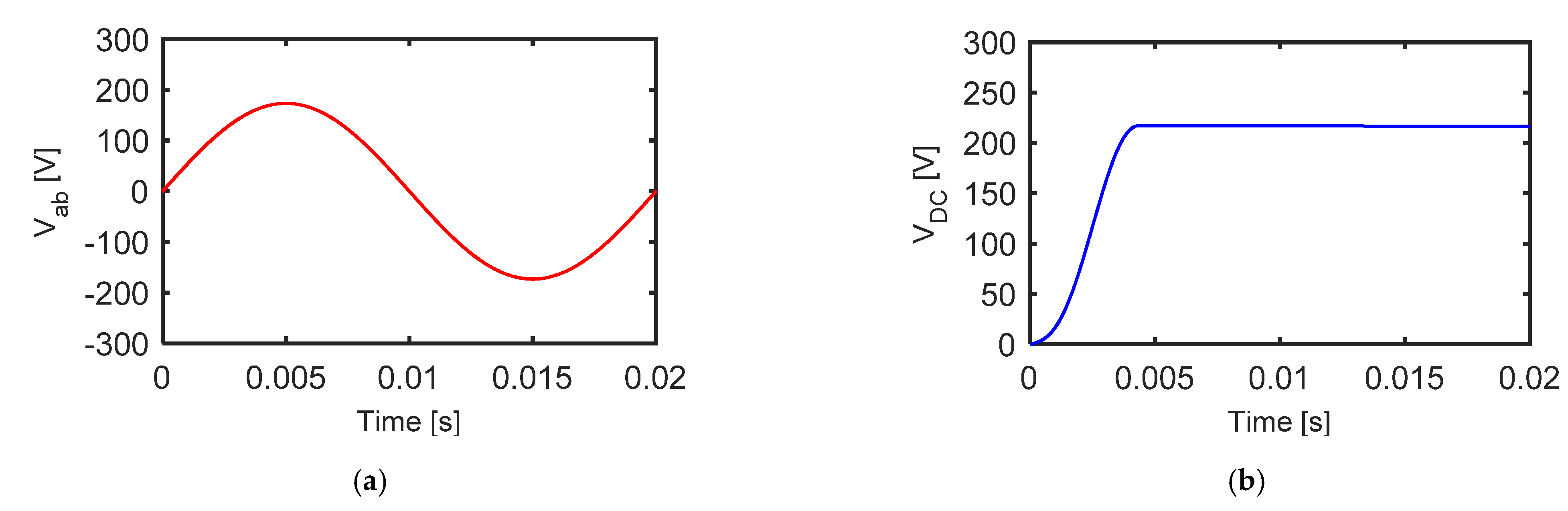
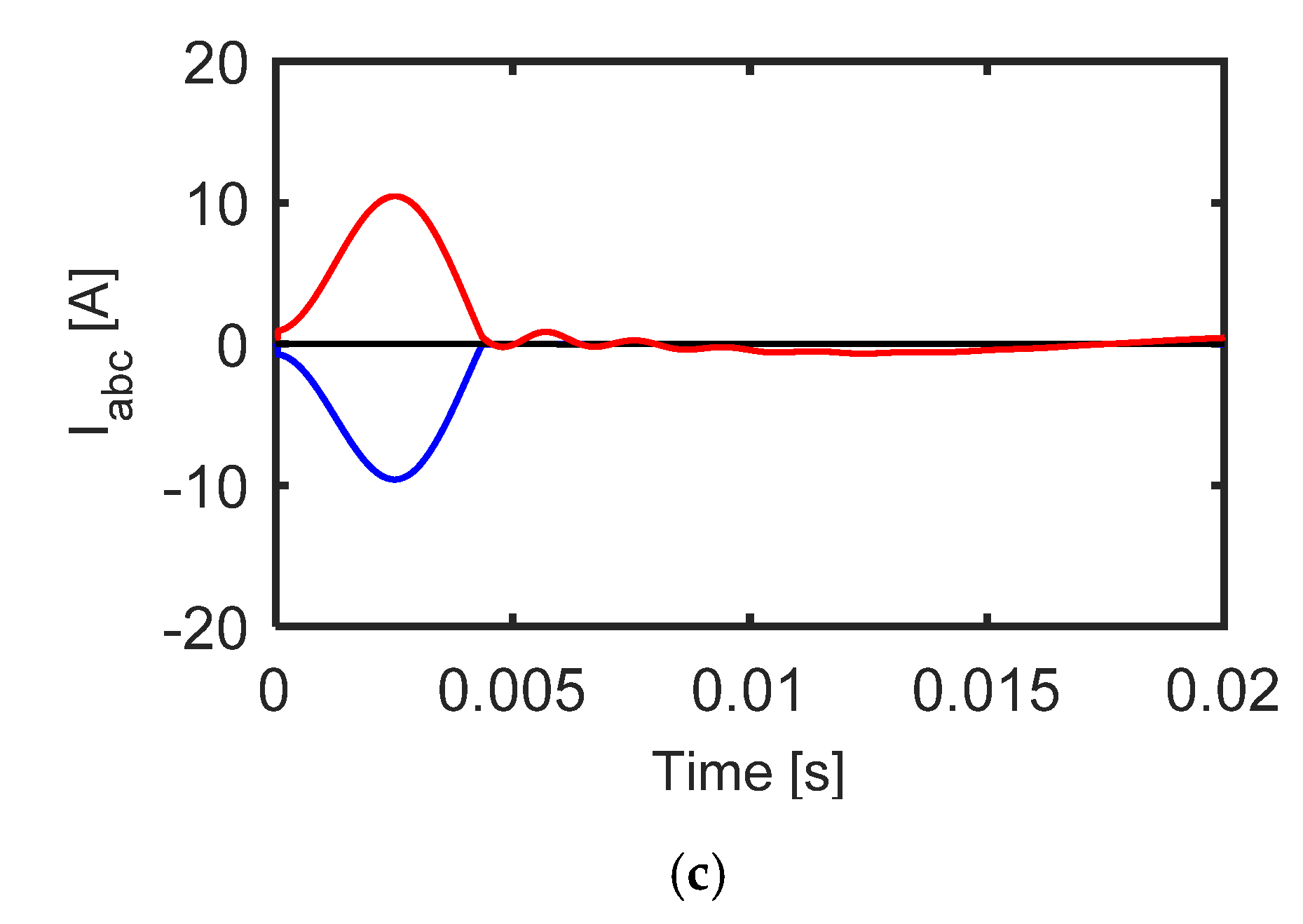
Figure 9.
Experimental testing of the clamping circuit at start-up without operating the PWM of the rectifier and charging using ramp-line voltage Vab (a) Line-input voltage Vab, (b) DC-link voltage and (c) input current for MC.
Figure 9.
Experimental testing of the clamping circuit at start-up without operating the PWM of the rectifier and charging using ramp-line voltage Vab (a) Line-input voltage Vab, (b) DC-link voltage and (c) input current for MC.
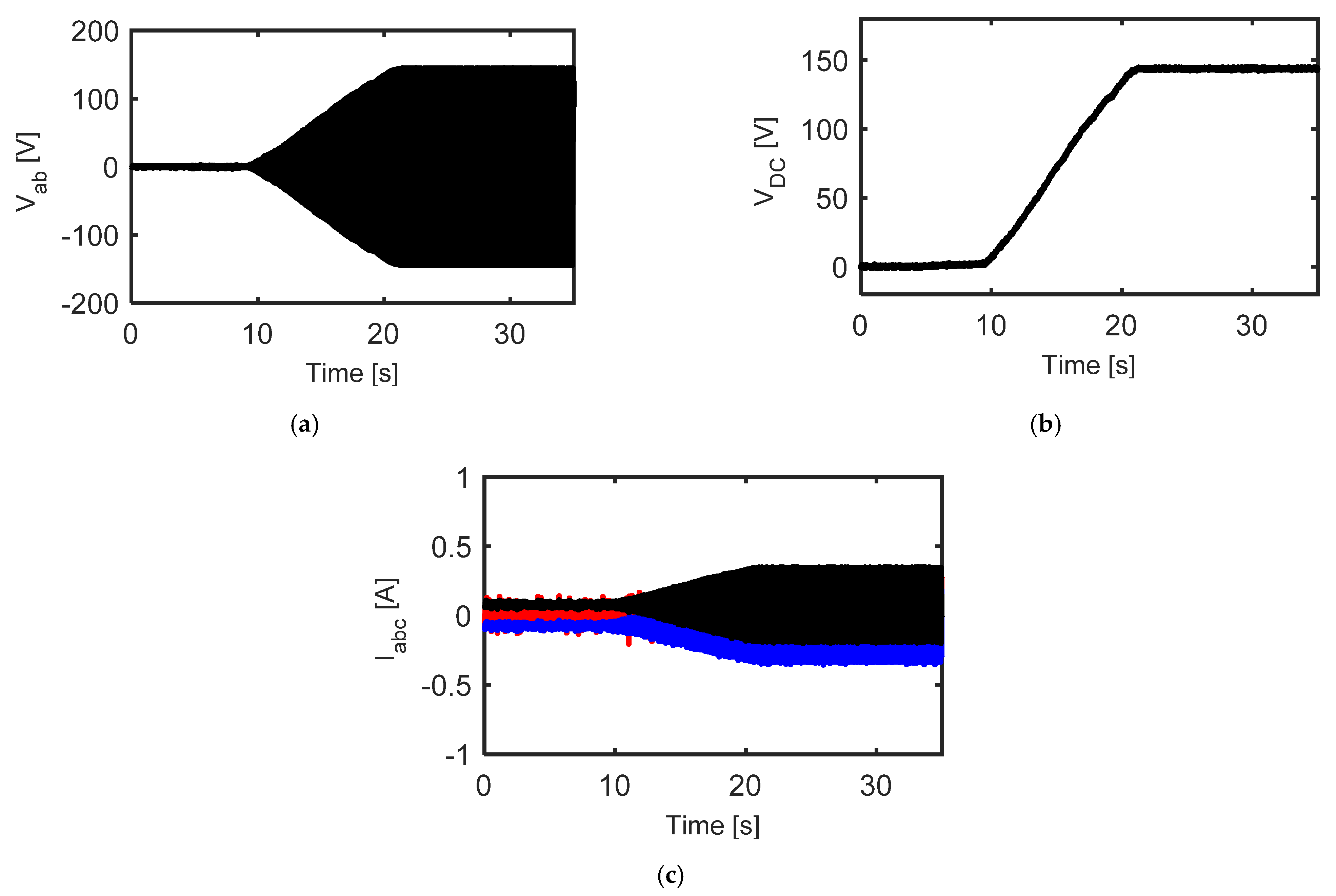
Figure 10.
Experimental testing of the clamping circuit at start-up without operating the PWM of the rectifier and charging using step-input-line voltage Vab (a) Line-input voltage Vab, (b) DC-link voltage, (c) input current for MC and (d) zoom-in view of the input current at start-up.
Figure 10.
Experimental testing of the clamping circuit at start-up without operating the PWM of the rectifier and charging using step-input-line voltage Vab (a) Line-input voltage Vab, (b) DC-link voltage, (c) input current for MC and (d) zoom-in view of the input current at start-up.
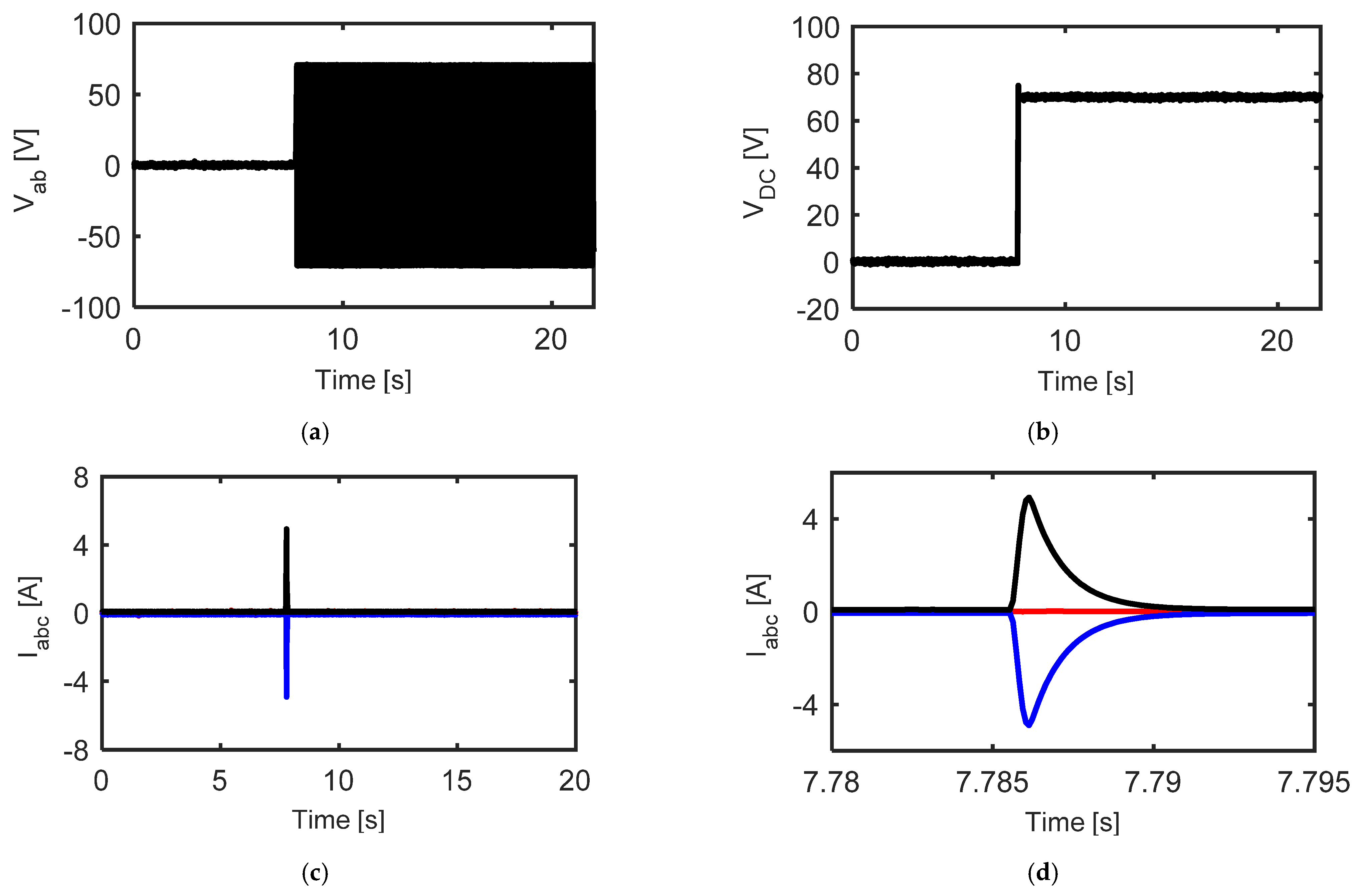
Figure 11.
Low-pass input filter.
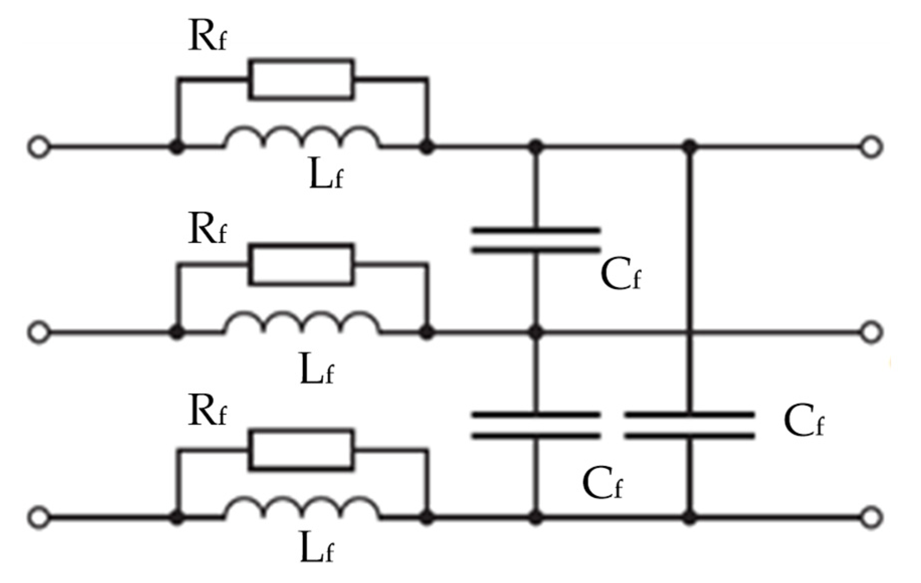
Figure 12.
The test bench.
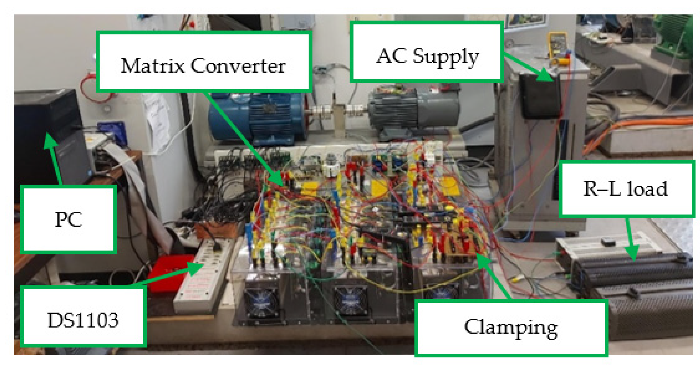
Figure 13.
Simulation results at 50 Hz output frequency (a) voltage of the DC link, (b) output line voltage, (c) output phase voltage and (d) output phase currents.
Figure 13.
Simulation results at 50 Hz output frequency (a) voltage of the DC link, (b) output line voltage, (c) output phase voltage and (d) output phase currents.
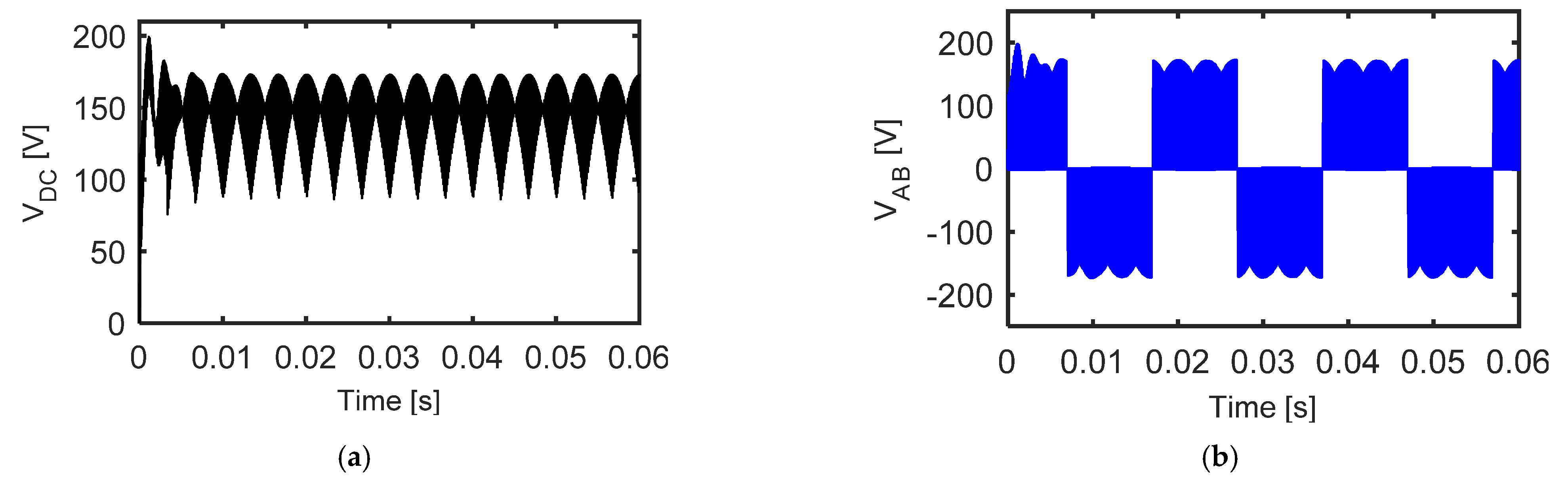

Figure 14.
Experimental results at 50 Hz output frequency (a) output line voltage, (b) output phase voltage and (c) output phase currents.
Figure 14.
Experimental results at 50 Hz output frequency (a) output line voltage, (b) output phase voltage and (c) output phase currents.
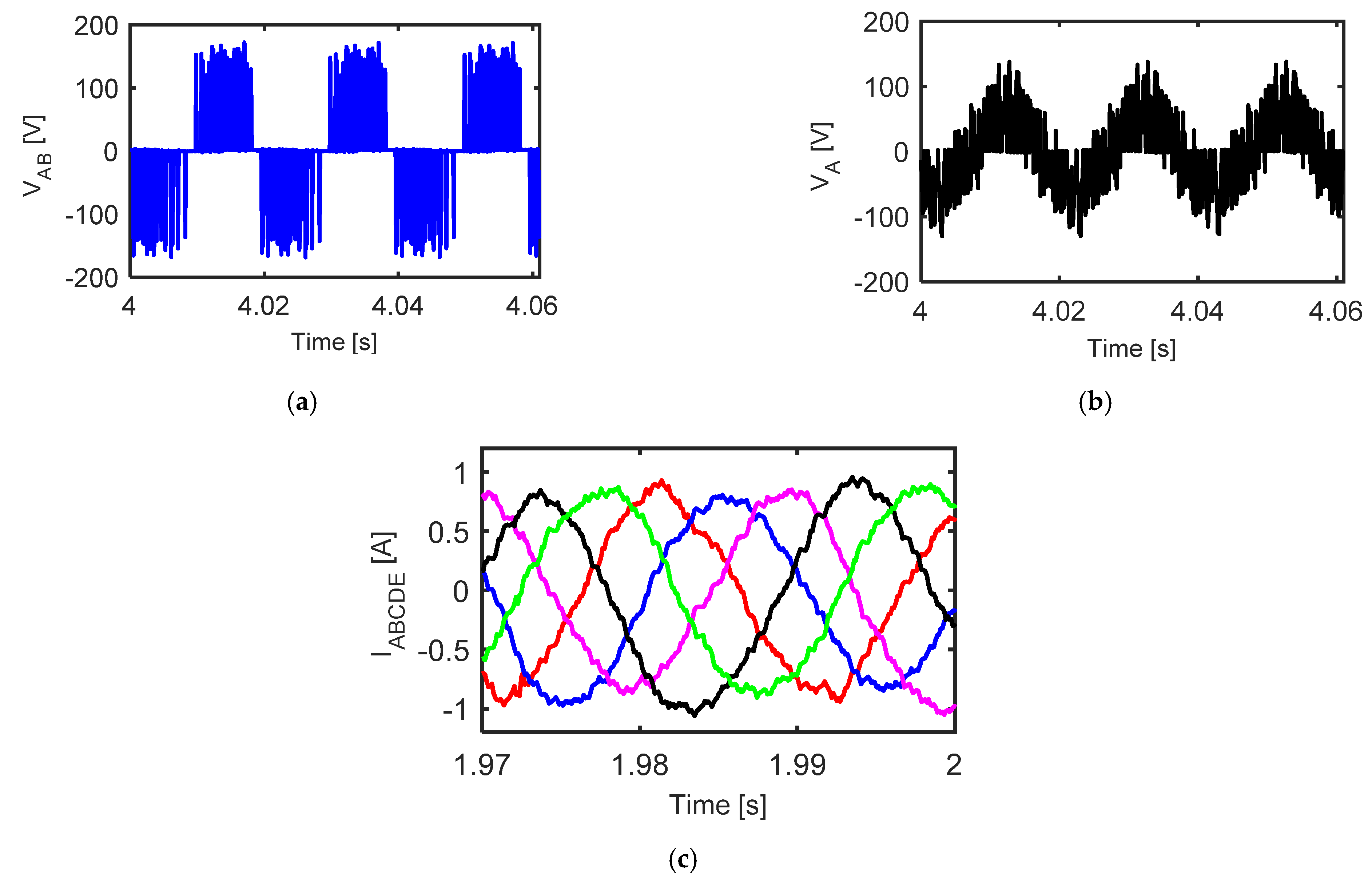
Figure 15.
Experimental results (a) phase input voltages and (b) the voltage of DC link.

Figure 16.
Simulation results at 100 Hz output frequency (a) output line voltage, (b) output phase voltage and (c) output phase currents.
Figure 16.
Simulation results at 100 Hz output frequency (a) output line voltage, (b) output phase voltage and (c) output phase currents.
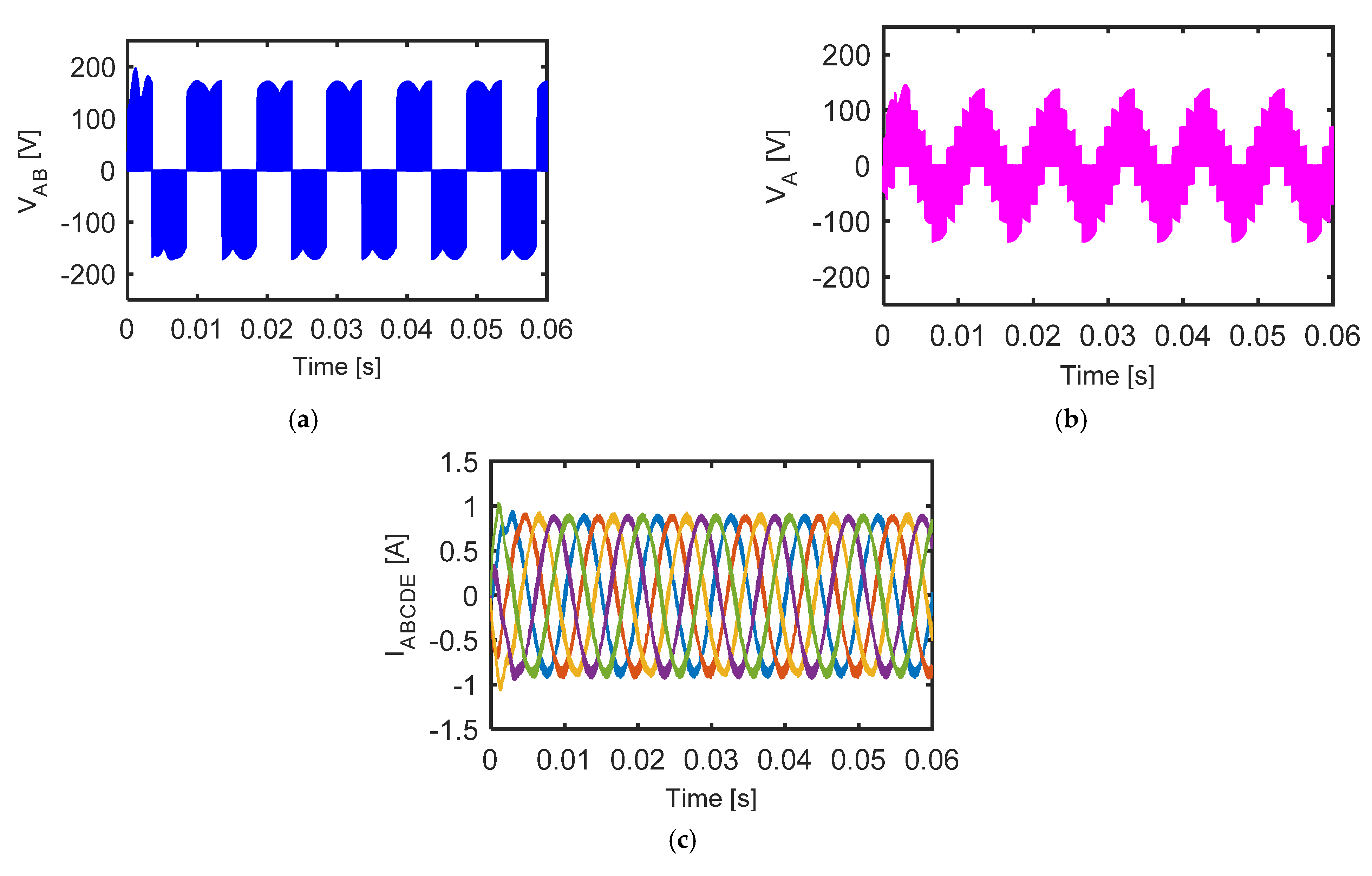
Figure 17.
Experimental results at 100 Hz output frequency (a) output line voltage, (b) output phase voltage and (c) output phase currents.
Figure 17.
Experimental results at 100 Hz output frequency (a) output line voltage, (b) output phase voltage and (c) output phase currents.
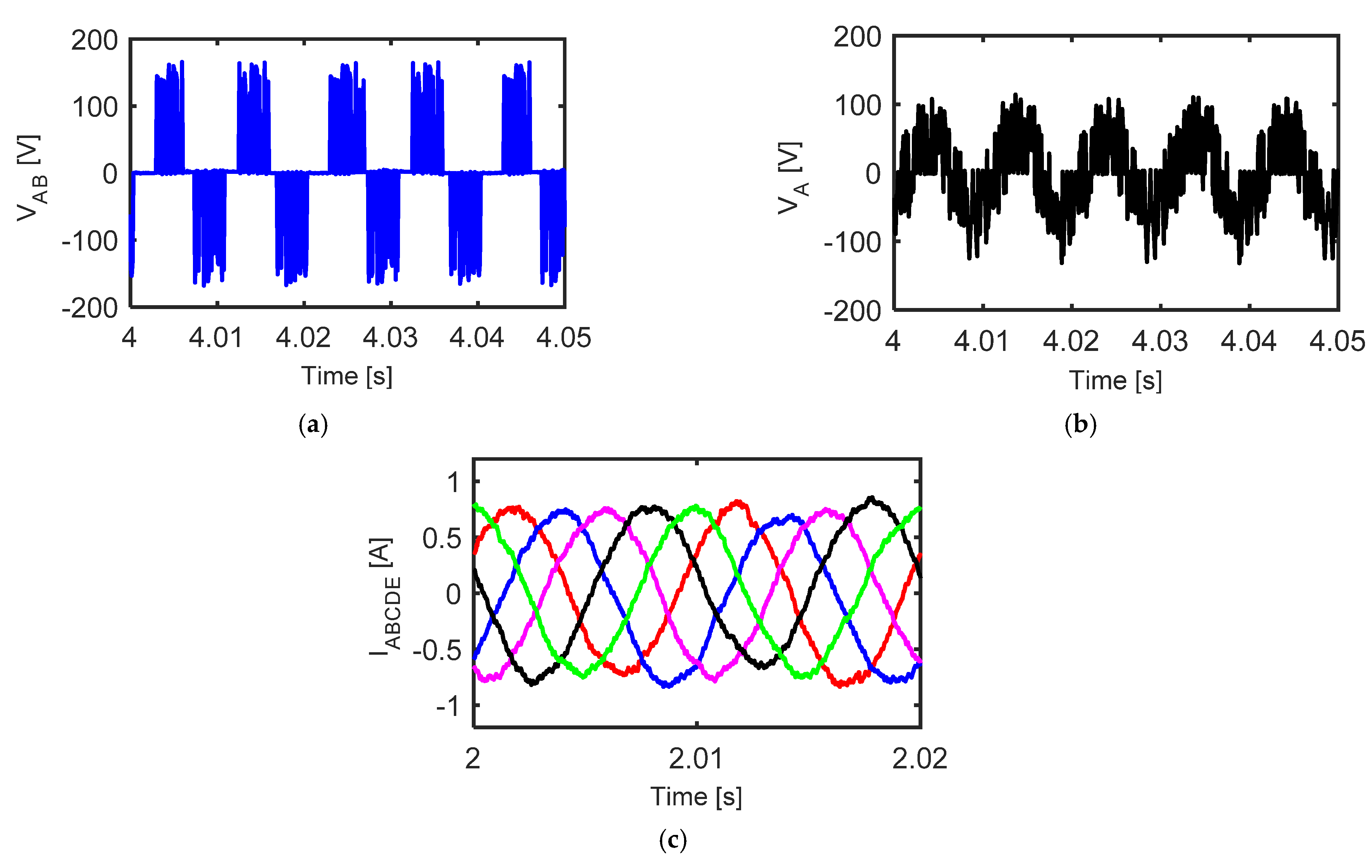
Figure 18.
Simulation results at 25 Hz output frequency (a) output line voltage, (b) output phase voltage and (c) output phase currents.
Figure 18.
Simulation results at 25 Hz output frequency (a) output line voltage, (b) output phase voltage and (c) output phase currents.

Figure 19.
Experimental results at 25 Hz output frequency (a) output line voltage, (b) output phase voltage and (c) output phase currents.
Figure 19.
Experimental results at 25 Hz output frequency (a) output line voltage, (b) output phase voltage and (c) output phase currents.

Table 1.
The switching states, the duty cycles, and the DC-link voltage for the rectifier in all sectors.
Table 1.
The switching states, the duty cycles, and the DC-link voltage for the rectifier in all sectors.
| Sector Number | ON Switch | The Duty Cycles and Modulated Switches | DC-Link Voltage | |||
|---|---|---|---|---|---|---|
| 1 | ||||||
| 2 | ||||||
| 3 | ||||||
| 4 | ||||||
| 5 | ||||||
| 6 | ||||||
Table 2.
Inverter’s switching vectors, which minimize switching losses in all sectors.
| Sector No. | ||||||
|---|---|---|---|---|---|---|
| 1 | V11 (10000) | V1 (11001) | V12 (11101) | V2 (11000) | ||
| 2 | V13 (01000) | V2 (11000) | V3 (11100) | V12 (11101) | ||
| 3 | V13 (01000) | V4 (01100) | V3 (11100) | V14 (11110) | ||
| 4 | V15 (00100) | V4 (01100) | V5 (01110) | V14 (11110) | ||
| 5 | V15 (00100) | V6 (00110) | V5 (01110) | V16 (01111) | V31 (00000) | V32 (11111) |
| 6 | V17 (00010) | V6 (00110) | V7 (00111) | V16 (01111) | ||
| 7 | V17 (00010) | V8 (00011) | V7 (00111) | V18 (10111) | ||
| 8 | V19 (00001) | V8 (00011) | V9 (10011) | V18 (10111) | ||
| 9 | V19 (00001) | V10 (10001) | V9 (10011) | V20 (11011) | ||
| 10 | V11 (10000) | V10 (10001) | V1 (11001) | V20 (11011) |
Publisher’s Note: MDPI stays neutral with regard to jurisdictional claims in published maps and institutional affiliations. |
© 2022 by the authors. Licensee MDPI, Basel, Switzerland. This article is an open access article distributed under the terms and conditions of the Creative Commons Attribution (CC BY) license (https://creativecommons.org/licenses/by/4.0/).
Share and Cite
MDPI and ACS Style
Tawfiq, K.B.; Ibrahim, M.N.; Sergeant, P. A Simple Commutation Method and a Cost-Effective Clamping Circuit for Three-to-Five-Phase Indirect-Matrix Converters. Electronics 2022, 11, 808. https://doi.org/10.3390/electronics11050808
AMA Style
Tawfiq KB, Ibrahim MN, Sergeant P. A Simple Commutation Method and a Cost-Effective Clamping Circuit for Three-to-Five-Phase Indirect-Matrix Converters. Electronics. 2022; 11(5):808. https://doi.org/10.3390/electronics11050808
Chicago/Turabian StyleTawfiq, Kotb B., Mohamed N. Ibrahim, and Peter Sergeant. 2022. "A Simple Commutation Method and a Cost-Effective Clamping Circuit for Three-to-Five-Phase Indirect-Matrix Converters" Electronics 11, no. 5: 808. https://doi.org/10.3390/electronics11050808
Note that from the first issue of 2016, this journal uses article numbers instead of page numbers. See further details here.