A High-Loop-Gain Low-Dropout Regulator with Adaptive Positive Feedback Compensation Handling 1-A Load Current

1
Institute of Microelectronics of the Chinese Academy of Sciences, Beijing 100029, China
2
University of Chinese Academy of Sciences, Beijing 100049, China
*
Author to whom correspondence should be addressed.
Electronics 2022, 11(6), 949; https://doi.org/10.3390/electronics11060949
Submission received: 14 February 2022
/
Revised: 11 March 2022
/
Accepted: 17 March 2022
/
Published: 18 March 2022
Abstract
:Low-dropout regulators, which have the capabilities of handling large output current and obtaining a superior transient response, are receiving increasing attention. This paper presents a high-output-current low-dropout regulator with high loop gain. An adaptive positive feedback compensation method is presented. It guarantees stability under full load conditions and achieves high loop gain. Without relying on an external zero, a ceramic capacitor with low equivalent series resistance can be employed, resulting in the minimized output voltage variation during the load transient response. In addition, the load regulation and line regulation are both small. An impedance adapting stage is inserted between the error amplifier and power transistor. It is suitable for low-supply voltage applications and drives the power transistor quickly. The simulation results indicate that the proposed LDO can supply a 1000 mA load current with a 200 mV dropout voltage. The load regulation and line regulations are 0.089 μV/mA and 0.562 m V/V, respectively. The power supply rejection is above 75 dB at 1 kHz under the full range of the output current.
1. Introduction
Power management is a necessary block for all electronic systems. Linear regulators have simpler circuit complexity, faster response, and lower noise content, compared with their switching counterparts [1,2,3]. The increasing growth in portable point-of-sale systems, Wi-Fi access points, and communication modules has fueled the growth of the low-dropout voltage regulators to handle large output current (about 1 A) [4]. Due to the dropout requirements, stability, and related inefficiency, designing a separate LDO for high-current applications is still a challenge.
The N-type LDO, in which an NMOS or NPN power transistor is adopted, has a faster transient response and less silicon real estate than the P-type LDO because of the inherent low impedance and high carrier mobility. The main disadvantage of the N-type LDO is the high-dropout voltage [5,6,7,8]. An extra internal charge pump or a second low-power input rail is needed to achieve a low-dropout voltage for N-type LDO [9,10]. For the P-type LDO, there are at least two low-frequency poles in the negative feedback loop: at the gate of the power transistor, and at the output of the LDO [11,12]. Many advanced structures aiming for high stability have been reported [13,14,15,16]. In [17,18], a dynamically biased buffer with shunt feedback has been adopted to drive the power transistor. When a larger load current (e.g., 1 A) is required, the buffer will dissipate a much larger quiescent current to push the parasitic pole to higher frequencies. However, this circuit is not suitable for low- applications due to the PMOS buffer and power stage [19]. A low-voltage LDO with damping-factor-control frequency compensation has been presented in [20], and a feedforward capacitor is employed to generate a left-half-plane (LHP) zero. The stability, output noise, and power-supply rejection ratio (PSRR) can be improved by using the feedforward capacitor [21], but the required reference voltage should be much smaller than the LDO output voltage, which limits the output range. Q-reduction frequency compensation has been proposed in [22], while the ESR of the off-chip capacitor is needed to introduce an LHP zero. Consequently, variations in the zero’s location across process and temperature may lead to instability. The ESR is also detrimental to the load transient performance. Active frequency compensation techniques, such as impedance adapting compensation [23], adaptive miller compensation [24], and pole-tracking compensation [25,26], may suffer from tracking accuracy under the wide range of the load current. The loop response determines the performance of an LDO greatly, such as loop gain and unity-gain frequency (UGF). Wider UGF improves the transient response, usually resulting in larger quiescent current and worse regulation accuracy [27,28]. Digital LDOs can achieve fast transient responses, but the maximum load current is usually small [29,30].
In this paper, a large-output-current LDO employing adaptive positive feedback compensation is proposed. A non-inverting driver stage with adaptive impedance is introduced for low-voltage applications. This paper is organized as follows: Section 2 presents the LDO structure with the proposed driver stage. In addition, loop stability analysis and details of the LDO circuit design considerations are illustrated. Section 3 provides simulation results and a comparison with previous studies. Finally, a conclusion is drawn.
2. Proposed Structure
Figure 1 shows the structure of the proposed LDO with adaptive positive feedback frequency compensation, which consists of a voltage reference , an error amplifier EA1, a non-inverting driver, and a pass transistor. The small-signal output resistor of the buffer is inversely proportional to the output current, which will lead to a load-dependent LHP zero. As the phase from V1 to Vg is non-inverting, the buffer and the capacitor Cc form the adaptive positive feedback compensation. A Miller capacitor Cf is used to create the dominant pole and realize the current buffer compensation. The bias current of the non-inverting driver is proportional to the load current so that the impedance at Vg can be decreased with the increase in the output current. It contributes to a better PSR performance without a complex circuit.
2.1. Non-Inverting Driver Stage
The proposed driver stage with adaptive impedance is shown in Figure 2. The first stage has a small signal gain and consists of transistors , and the constant current source . The second stage consists of transistors , and the constant current source . The minimum supply voltage of this structure is about to provide a large load current. Transistor realizes a dynamically biased load by sensing the output current in the pass transistor . At light conditions, the current in is small, while is biased in the subthreshold region because the width of is large. As the load current increases, the bias current in increases, and the small output impedance to ground at node decreases. Due to the diode-connected structure of , the parasitic pole frequency at node is far beyond the UGF of the whole loop.
In addition, the current mirror structure of the second driving stage allows the LDO to achieve better PSR performance without any complex circuitry. The driver stage is a non-inverting stage, thus forming the proposed adaptive positive feedback compensation with the compensate capacitor Cc.
2.2. Adaptive Positive Feedback Compensation
Figure 3 shows the transistor level schematic of the proposed LDO structure; the first stage of the error amplifier is realized by a single-stage folded-cascode structure, with transistors . As discussed before, the driving stage can be viewed as a non-inverting, single stage. Accordingly, the LDO structure can be modeled as a three-stage amplifier in which the third stage is realized by the pass transistor . A microfarad range off-chip capacitor is used at the output of the LDO. The adaptive positive feedback compensation scheme creates a real LHP zero and allows the LDO to achieve higher stability with a lower quiescent current. and form the inverting buffer, in which the output is in series with capacitor Cc. The buffer has an adaptive output resistance, as the current in is proportional to the output current in . , ,, and the inverting buffer realize the compensation circuit of the proposed LDO. The loop stability and design considerations are discussed in what follows.
In order to study the stability of the LDO, the loop transfer function is derived. Figure 4 shows the small-signal block diagram representation of the structure in Figure 3. Hence, , , , and represent the transconductance of the input differential transistor pair , the non-inverting driver stage, power transistor , and transistor , respectively. The transconductance of is expressed as , and the small-signal output resistance of the buffer is inversely proportional to , which can be expressed as
In addition, the output impedance of each stage is denoted as The lumped parasitic capacitances at nodes are modeled as , and , respectively. The feedback factor B = 1 is used to derive the loop gain function. The loop transfer function will be derived and simplified based on the following considerations:
- is much larger than other capacitors;
- , , are much larger than .
The loop-gain transfer function of the proposed LDO can be written as
From (3), the transfer function is negative due to the negative feedback. The low-frequency loop gain can be expressed as T0. Under a full range of the load current, the numerator of T(s) indicates that two real LHP zeros exit since. The denominator of T(s) implies that four poles exit. is the dominant pole, and is the second pole, with , , given in (8) and (9). The loop stability should be studied for different load conditions.
At light load conditions, is rather small, and . Two LHP zeros are and Besides the dominant pole and the second pole , the third pole is , and the fourth pole is . Hence, and cancel each other. The ratio of indicates that is larger than . The parasitic pole can be neglected due to the large . In this case, the unity-gain frequency and phase margin PM of the system are given by
At medium-to-heavy load conditions, is much large and . The third pole is , and the fourth pole is . Two LHP zeros are and Due to the large , is quite larger than and . Thus, is fixed and extends the UGF. The LDO loop thus acts as a first-order system and the stability of the LDO can be guaranteed.
At certain load conditions, is close to . The transfer function can be revised as
From (13), the parameter m is close to 0 due to the large , resulting in conjugate poles and . Consequently, and are far beyond the two LHP zeros and . Large is helpful to push the conjugate poles to higher frequencies while having a detrimental effect on the load transient response. In addition, large may cause frequency peaks at light load conditions. By setting , the LDO can achieve a good compromise between stability and transient response.
Figure 5 depicts the simulated loop gain of the proposed LDO under different load currents. The DC loop gain is above 100 dB under full load conditions and the bandwidth increases with load current. The phase margin at no-load and full-load conditions are 52° and 94°, respectively. Process corner and temperature simulation are also implemented to prove the feasibility of the proposed compensation technique. As shown in Figure 6, for different process corners and temperatures, the phase margin of the proposed LDO is above 35° under the full range of load currents. Monte Carlo simulation of phase margin at worst stability, i.e., Iload = 1 mA is shown in Figure 7. Thus, stability is guaranteed over the full load current range.
2.3. Circuit Design Considerations
As discussed before, the main source of the operating supply current is derived from and . The ratio of to is . The large indicates that a small dynamic current is required, which results in a high current efficiency under heavy load conditions. A 1.2 V internal voltage reference is integrated with the LDO to provide the reference voltage to the input of the error amplifier. In the proposed LDO, the gain of the error amplifier is always greater than 60 dB under the entire load current range. Under the no-load condition, the pass transistor is in the subthreshold region, as it only provides current for the feedback resistors and . Adjustable output can be realized by changing the ratio of the feedback resistors and .The current is equal to , and the gate-source voltage required for to minimize the amount of current can be around 400 mV. A ceramic capacitor, which has a low ESR value, is desired for low-output overshoot/undershoot during the load transient response. In this design, a few mΩ resistors are in series with the 4.7 μF capacitor, to emulate the effects of a practical ceramic capacitor.
3. Simulation Results
The proposed LDO was designed and simulated in a 0.18 BCD process with 5 V NMOS and PMOS. Protect circuits and internal voltage reference circuits were integrated with the proposed LDO. The protect circuits consisted of overtemperature protect circuits, overcurrent protect circuits, and under-voltage locking circuits.t The total layout is shown in Figure 8; the whole chip area, including pads, is about 1184 μm × 1179 μm. The simulation results are presented below.
The input voltage range of the LDO was designed from 1.6 V to 5.5 V for portable applications. The LDO can deliver up to 1 A with a dropout voltage of 0.2 V. Since the proposed LDO does not rely on the ESR zero, a ceramic 4.7 capacitor was used to minimize load transient dips caused by ESR. The LDO was also stable for output capacitor values of 4.7 to 22. In addition, the LDO consumed a small quiescent current of 21 μA under the no-load condition, while the quiescent current of 424was dissipated at full load condition. The current efficiency was 99.9% at full load condition.
High loop gain allows the LDO to achieve superior regulation. The load and line regulations were 0.089 μV/mA and 0.81 mV/V, respectively. Figure 9 depicts the PSR of the LDO under different load currents when = 1.6 V and= 1.2 V. The PSR benefitted from the high loop gain and the current-mirror load structure used in the driving stage. In addition, the 4.7 output capacitor dampened the peaking effects in the PSR curves, resulting in the improved PSR performance at high frequency.
Figure 10 shows the simulated transient response when the load current switched between 0.1 A and 1 A with 1 rise/fall time. The maximum output voltage overshoot and undershoot were both less than 30 mV when was at 1.2 V. Small transient variation under massive load-step change was obtained, which results from both the proposed adaptive impedance driving stage and positively adaptive feedback compensation. Otherwise, a large phase margin allowed the LDO to achieve a well-behaved settling characteristic.
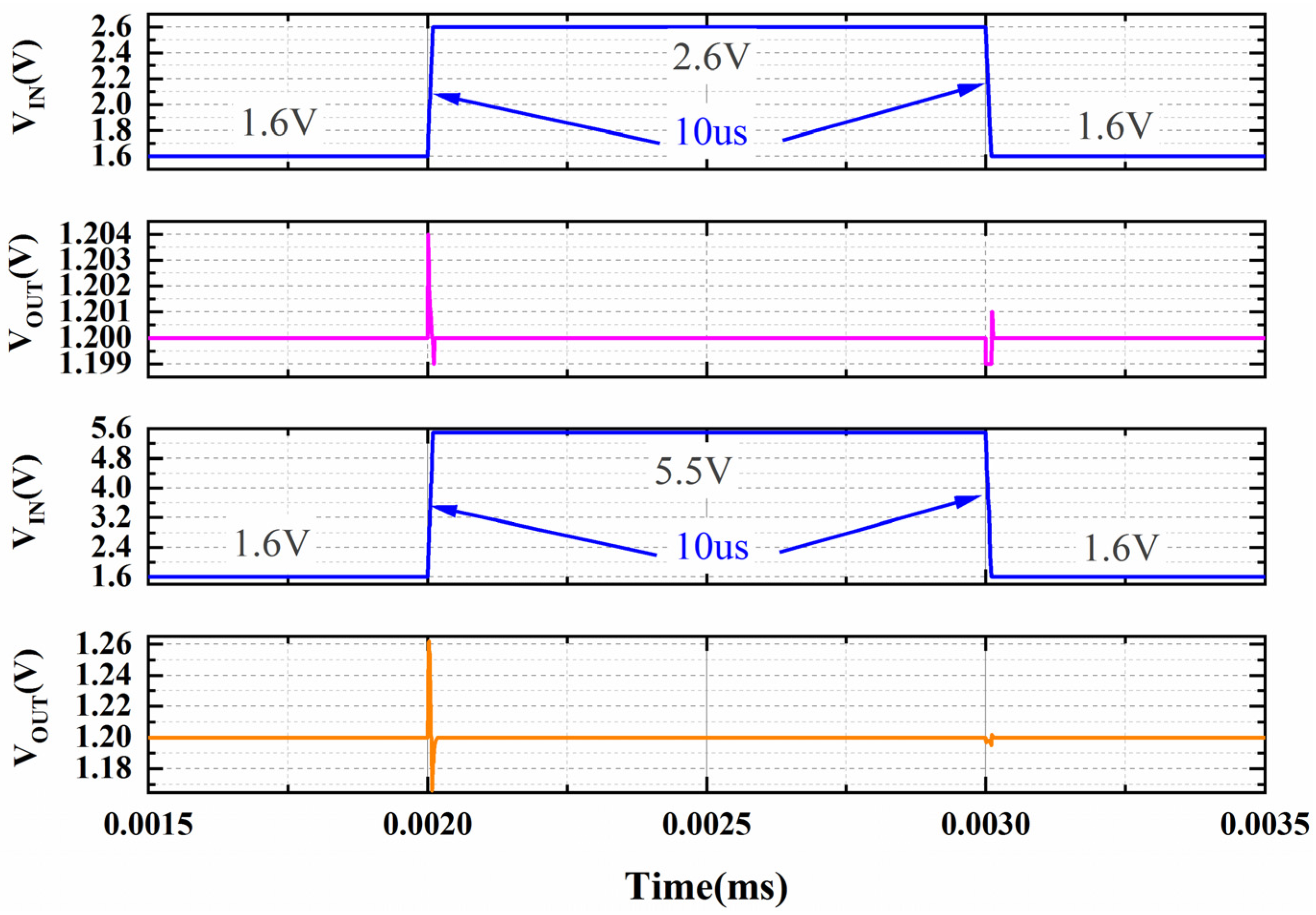
The line transient response is given in Figure 11, according to which the implication of input voltage varied on the output voltage. When the change in the input voltage was from 1.6 V to 5.5 V with 10 rise and fall time, the output voltage changed by less than 100 mV at = 0.2 A. When the change in the input voltage was from 1.6 V to 2.6 V with 10 rise and fall time, the output voltage changed by less than 5.5 mV at = 0.2 A.
In order to provide a clear picture of the performance improvement in the proposed LDO resulting from the adaptive impedance driving stage and adaptive positive feedback frequency compensation technique, a comparison with some reported LDOs in terms of performance is given in Table 1. A Figure of merit [18] is introduced to compare the transient response of different LDOs, in which , , , and represent the output capacitor, quiescent current, the output voltage variation due to the load switch, and the maximum load current step, respectively. Smaller FOM means a better level of transient performance of the LDO [31]. From Table 1, it is revealed that the proposed LDO achieved lower FOM and higher load regulation, compared with other reported LDOs.
4. Conclusions
In this paper, a high-output current (1 A) LDO with adaptive positive feedback compensation was proposed. The proposed compensation technique ensures loop stability under the full range of load currents. In addition, high loop gain was achieved, resulting in low load regulation. A driver stage that is suitable for low-supply voltage applications was also applied. It improved the driving ability of the power transistor so that enhances the transient response. The simulation results show that the overshoot and undershoot voltage of the output were both less than 30 mV when the load current varied from 0.1 to 1 A. Compared with other studies in the literature, the proposed LDO had lower FOM.
Author Contributions
Conceptualization, Y.J. and L.W.; methodology, Y.J. and Y.W.; software, Y.J. and S.W.; writing—original draft preparation, Y.J. and Y.W.; writing—review and editing, Y.J. and M.G. All authors have read and agreed to the published version of the manuscript.
Funding
This research received no external funding.
Data Availability Statement
No new data were created or analyzed in this study. Data sharing is not applicable to this paper.
Acknowledgments
The authors would like to express their appreciation to all members of the New technology development department.
Conflicts of Interest
The authors declare no conflict of interest.
References
- Ming, X.; Kuang, J.J.; Liang, H.; Zhang, J.; Qin, Y.; Zhang, Z.W.; Wang, Z.; Zhang, B. A Fast-Transient Low-Dropout Regulator with Current-Efficient Super Transconductance Cell and Dynamic Reference Control. IEEE Trans. Circuits Syst. I Regul. Pap. 2021, 68, 2354–2367. [Google Scholar] [CrossRef]
- Huang, C.H.; Ma, Y.T.; Liao, W.C. Design of a Low-Voltage Low-Dropout Regulator. IEEE Trans. Very Large Scale Integr. VLSI Syst. 2014, 22, 1308–1313. [Google Scholar] [CrossRef]
- Lu, Y.; Wang, Y.P.; Pan, Q.; Ki, W.H.; Yue, C.P. A Fully-Integrated Low-Dropout Regulator With Full-Spectrum Power Supply Rejection. IEEE Trans. Circuits Syst. I Regul. Pap. 2015, 62, 707–716. [Google Scholar] [CrossRef]
- Xu, W.; Upadhyaya, P.; Wang, X.; Tsang, R.; Lin, L. A 1A LDO Regulator Driven by a 0.0013mm(2) Class-D Controller. In Proceedings of the 2017 IEEE International Solid-State Circuits Conference (ISSCC), San Francisco, CA, USA, 5–9 February 2017; p. 104. [Google Scholar]
- Duan, Q.; Li, W.; Huang, S.; Ding, Y.; Meng, Z.; Shi, K. A Two-Module Linear Regulator with 3.9-10 V Input, 2.5 V Output, and 500 mA Load. Electronics 2019, 8, 1143. [Google Scholar] [CrossRef] [Green Version]
- Li, K.; Yang, C.; Guo, T.; Zheng, Y. A Multi-Loop Slew-Rate-Enhanced NMOS LDO Handling 1-A-Load-Current Step with Fast Transient for 5G Applications. IEEE J. Solid-State Circuits 2020, 55, 3076–3086. [Google Scholar] [CrossRef]
- Mandal, D.; Desai, C.; Bakkaloglu, B.; Kiaei, S. Adaptively Biased Output Cap-Less NMOS LDO With 19 ns Settling Time. IEEE Trans. Circuits Syst. II Express Briefs 2019, 66, 167–171. [Google Scholar] [CrossRef]
- Duong, Q.-H.; Huy-Hieu, N.; Kong, J.-W.; Shin, H.-S.; Ko, Y.-S.; Yu, H.-Y.; Lee, Y.-H.; Bea, C.-H.; Park, H.-J. Multiple-Loop Design Technique for High-Performance Low-Dropout Regulator. IEEE J. Solid-State Circuits 2017, 52, 2533–2549. [Google Scholar] [CrossRef]
- Magod, R.; Bakkaloglu, B.; Manandhar, S. A 1.24 mu A Quiescent Current NMOS Low Dropout Regulator With Integrated Low-Power Oscillator-Driven Charge-Pump and Switched-Capacitor Pole Tracking Compensation. IEEE J. Solid-State Circuits 2018, 53, 2356–2367. [Google Scholar] [CrossRef]
- Jiang, J.; Shu, W.; Chang, J.S. A 65-nm CMOS Low Dropout Regulator Featuring >60-dB PSRR Over 10-MHz Frequency Range and 100-mA Load Current Range. IEEE J. Solid-State Circuits 2018, 53, 2331–2342. [Google Scholar] [CrossRef]
- Milliken, R.J.; Silva-Martinez, J.; Sanchez-Sinencio, E. Full On-Chip CMOS Low-Dropout Voltage Regulator. IEEE Trans. Circuits Syst. I Regul. Pap. 2007, 54, 1879–1890. [Google Scholar] [CrossRef]
- Man, T.Y.; Mok, P.K.T.; Chan, M. A High Slew-Rate Push–Pull Output Amplifier for Low-Quiescent Current Low-Dropout Regulators with Transient-Response Improvement. IEEE Trans. Circuits Syst. II Express Briefs 2007, 54, 755–759. [Google Scholar] [CrossRef]
- Jeon, I.; Guo, T.; Roh, J. 300 mA LDO Using 0.94 mu A I-Q With an Additional Feedback Path for Buffer Turn-off Under Light-Load Conditions. IEEE Access 2021, 9, 51784–51792. [Google Scholar] [CrossRef]
- Lu, Y.; Ki, W.-H.; Yue, C.P. A 0.65ns-Response-Time 3.01ps FOM Fully-Integrated Low-Dropout Regulator with Full-Spectrum Power-Supply-Rejection for Wideband Communication Systems. In Proceedings of the 2014 IEEE International Solid-State Circuits Conference Digest of Technical Papers (ISSCC), San Francisco, CA, USA, 9–13 February 2014; pp. 306–307. [Google Scholar]
- Oh, W.; Bakkaloglu, B. A CMOS low-dropout regulator with current-mode feedback buffer amplifier. IEEE Trans. Circuits Syst. II Express Briefs 2007, 54, 922–926. [Google Scholar] [CrossRef]
- Zhan, C.; Ki, W.-H. An Output-Capacitor-Free Adaptively Biased Low-Dropout Regulator with Subthreshold Undershoot-Reduction for SoC. IEEE Trans. Circuits Syst. I Regul. Pap. 2012, 59, 1119–1131. [Google Scholar] [CrossRef]
- Al-Shyoukh, M.; Lee, H.; Perez, R. A transient-enhanced low-quiescent current low-dropout regulator with buffer impedance attenuation. IEEE J. Solid-State Circuits 2007, 42, 1732–1742. [Google Scholar] [CrossRef] [Green Version]
- Li, K.; Xiao, X.; Jin, X.; Zheng, Y. A 600-mA, Fast-Transient Low-Dropout Regulator with Pseudo-ESR Technique in 0.18-mu m CMOS Process. IEEE Trans. Very Large Scale Integr. VLSI Syst. 2020, 28, 403–413. [Google Scholar] [CrossRef]
- Park, J.; Lee, B.; Hong, S.-W. An Output Capacitorless Low-Dropout Regulator with a Low-V-DD Inverting Buffer for the Mobile Application. IEEE Trans. Ind. Electron. 2020, 67, 8931–8935. [Google Scholar] [CrossRef]
- Leung, K.N.; Mok, P.K.T. A capacitor-free CMOS low-dropout regulator with damping-factor-control frequency compensation. IEEE J. Solid-State Circuits 2003, 38, 1691–1702. [Google Scholar] [CrossRef]
- Hong, S.-W.; Cho, G.-H. High-Gain Wide-Bandwidth Capacitor-Less Low-Dropout Regulator (LDO) for Mobile Applications Utilizing Frequency Response of Multiple Feedback Loops. IEEE Trans. Circuits Syst. I Regul. Pap. 2016, 63, 46–57. [Google Scholar] [CrossRef]
- Lau, S.K.; Mok, P.K.T.; Leung, K.N. A Low-Dropout Regulator for SoC with Q-Reduction. IEEE J. Solid-State Circuits 2007, 42, 658–664. [Google Scholar] [CrossRef]
- Cao, H.; Yang, X.; Li, W.; Ding, Y.; Qu, W. An Impedance Adapting Compensation Scheme for High Current NMOS LDO Design. IEEE Trans. Circuits Syst. II Express Briefs 2021, 68, 2287–2291. [Google Scholar] [CrossRef]
- Lai, X.; Guo, J.; Sun, Z.; Xie, J. A 3-A CMOS low-dropout regulator with adaptive Miller compensation. Analog Integr. Circuits Signal Process. 2006, 49, 5–10. [Google Scholar] [CrossRef]
- Han, X.; Wu, L.; Gao, Y.; Ki, W.-H. An Adaptively Biased Output-Capacitor-Free Low-Dropout Regulator with Supply Ripple Subtraction and Pole-Tracking-Compensation. IEEE Trans. Power Electron. 2021, 36, 12795–12804. [Google Scholar] [CrossRef]
- Ming, X.; Liang, H.; Zhang, Z.-W.; Xin, Y.-L.; Qin, Y.; Wang, Z. A High-Efficiency and Fast-Transient Low-Dropout Regulator with Adaptive Pole Tracking Frequency Compensation Technique. IEEE Trans. Power Electron. 2020, 35, 12401–12415. [Google Scholar] [CrossRef]
- Bu, S.; Guo, J.; Leung, K.N. A 200-ps-Response-Time Output-Capacitorless Low-Dropout Regulator with Unity-Gain Bandwidth >100 MHz in 130-nm CMOS. IEEE Trans. Power Electron. 2018, 33, 3232–3246. [Google Scholar] [CrossRef]
- Ma, X.; Lu, Y.; Li, Q. A Fully Integrated LDO with 50-mV Dropout for Power Efficiency Optimization. IEEE Trans. Circuits Syst. II Express Briefs 2020, 67, 725–729. [Google Scholar] [CrossRef]
- Lv, S.P.; Wan, P.Y.; Zhang, H.D.; Geng, J.R.; Wen, J.B.; Yao, Y.M.; Chen, Z.J. A 0.18-ns Response Time Digital LDO Regulator with Adaptive PI Controller in 180-nm CMOS. Electronics 2021, 10, 1668. [Google Scholar] [CrossRef]
- Yu, Y.; Yuan, J.; Qiao, S.S.; Hei, Y. A Fast-Transient All-Digital LDO with Adaptive Clock Technique. Electronics 2019, 8, 1422. [Google Scholar] [CrossRef] [Green Version]
- Hazucha, P.; Karnik, T.; Bloechel, B.A.; Parsons, C.; Finan, D.; Borkar, S. Area-efficient linear regulator with ultra-fast load regulation. IEEE J. Solid-State Circuits 2005, 40, 933–940. [Google Scholar] [CrossRef]
- Ho, M.; Guo, J.; Mak, K.H.; Goh, W.L.; Bu, S.; Zheng, Y.; Tang, X.; Leung, K.N. A CMOS Low-Dropout Regulator With Dominant-Pole Substitution. IEEE Trans. Power Electron. 2016, 31, 6362–6371. [Google Scholar] [CrossRef]
- Choe, Y.-J.; Nam, H.; Park, J.-D. A Low-Dropout Regulator with PSRR Enhancement through Feed-Forward Ripple Cancellation Technique in 65 nm CMOS Process. Electronics 2020, 9, 146. [Google Scholar] [CrossRef] [Green Version]
- Zhang, H.D.; Wan, P.Y.; Geng, J.R.; Liu, Z.Z.; Chen, Z.J. A Fast Transient Response Digital LDO with a TDC-Based Signal Converter. Electronics 2020, 9, 132. [Google Scholar] [CrossRef] [Green Version]
Figure 1.
The proposed LDO structure with adaptive positive feedback compensation.
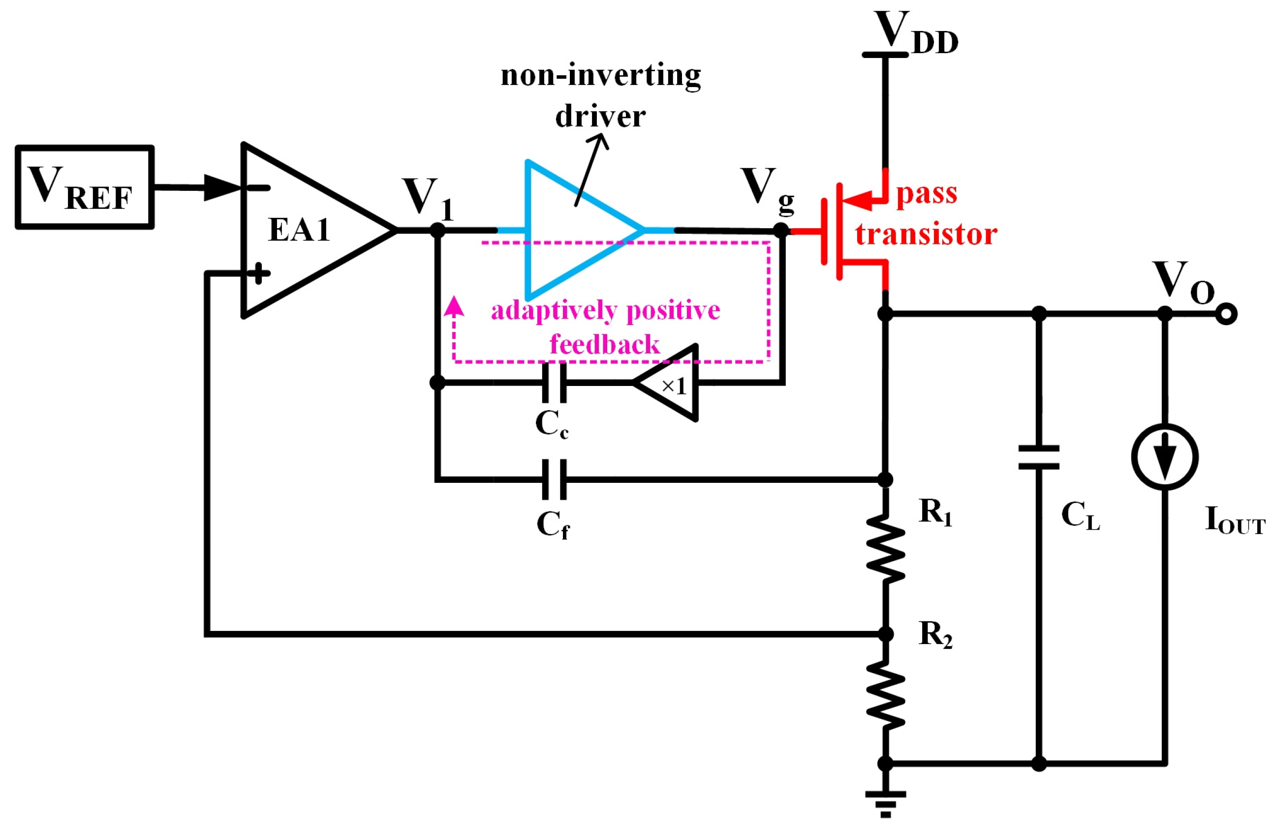
Figure 2.
The non-inverting driver stage used in the proposed LDO.
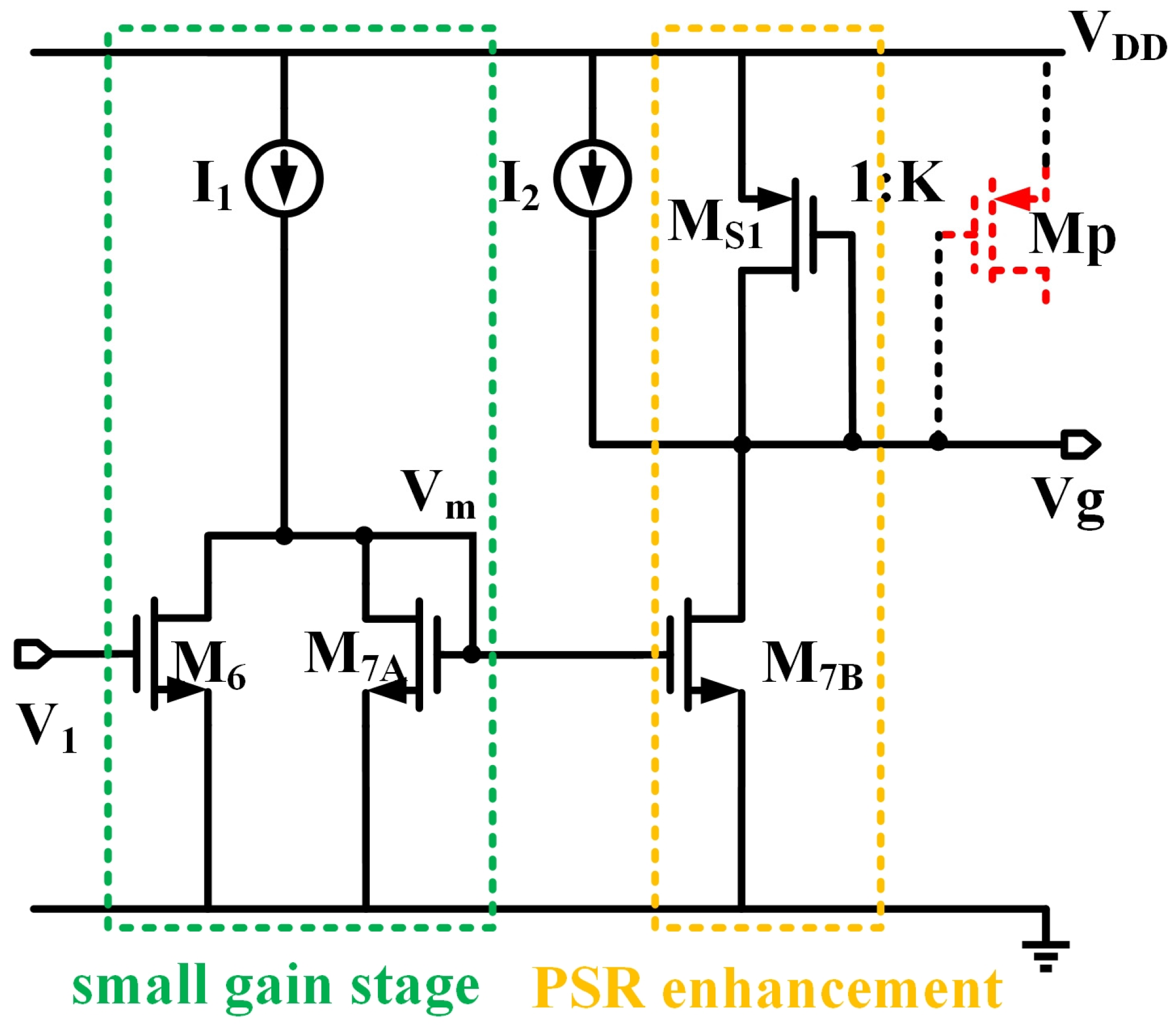
Figure 3.
Transistor level schematic of the proposed LDO.

Figure 4.
Small-signal block diagram of the proposed LDO.

Figure 5.
Simulated loop gain of the LDO under different load currents.

Figure 6.
Phase margin of the proposed LDO under different load currents, process corners, and temperatures.
Figure 6.
Phase margin of the proposed LDO under different load currents, process corners, and temperatures.
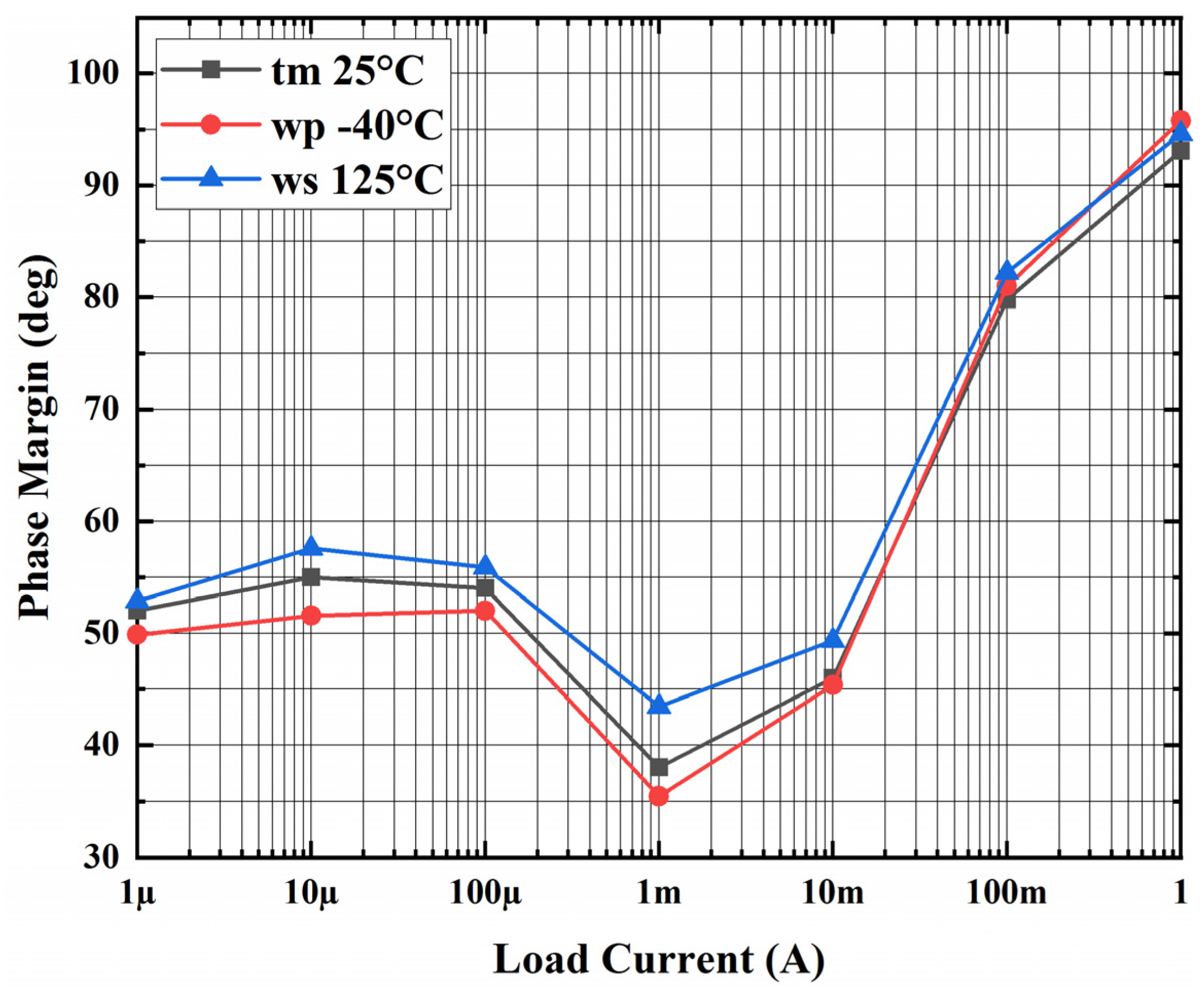
Figure 7.
Monte Carlo simulation results of phase margin at 1 mA load current.

Figure 8.
Layout of the proposed LDO.

Figure 9.
Simulated PSR of the LDO at different load conditions.
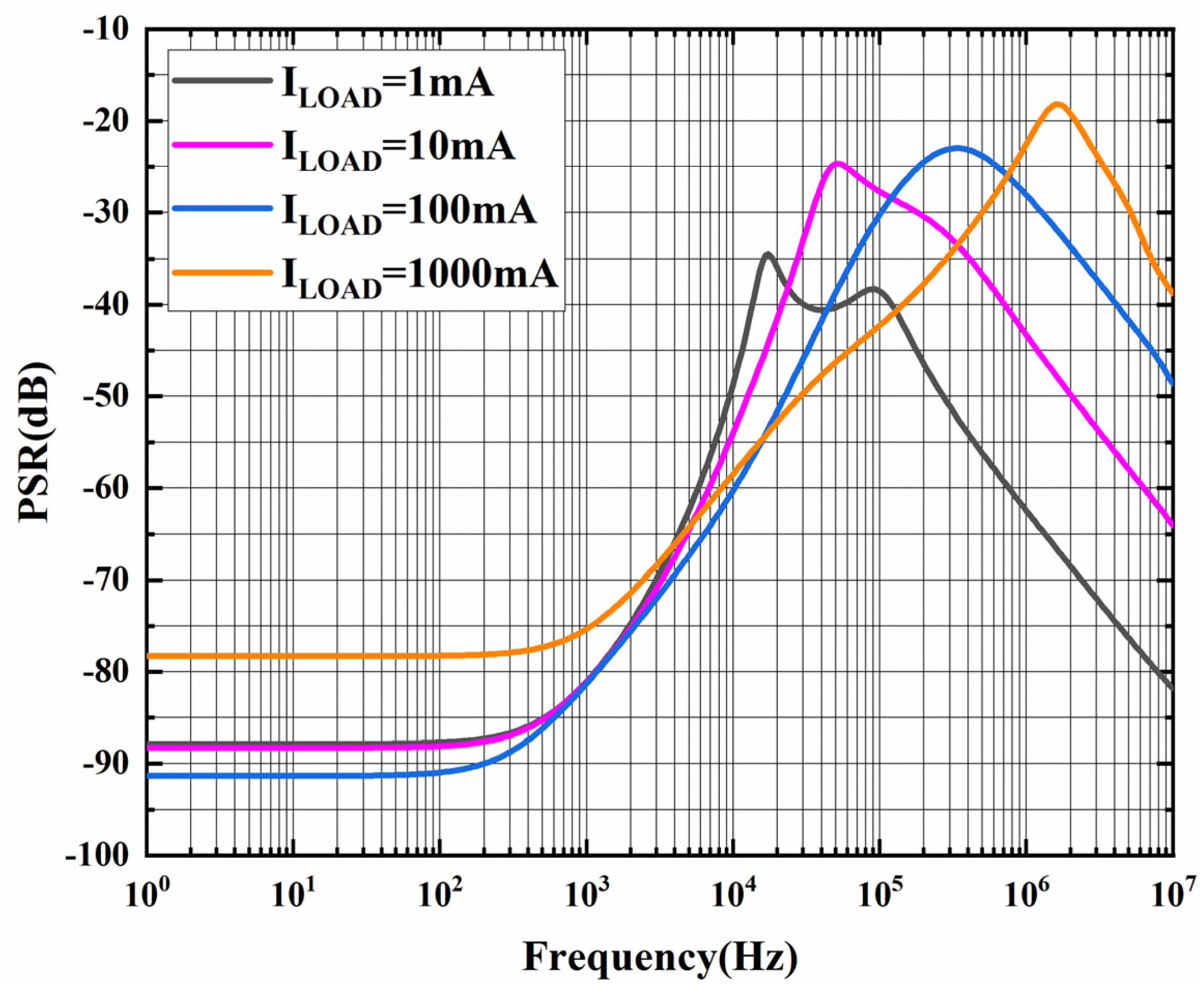
Figure 10.
Simulated load transient response with 900 mA.

Figure 11.
Simulated line transient response when input voltage change from 1.6 V to 5.5 V and 1.6 V to 5.5 V with a 10 transition-edge time.
Figure 11.
Simulated line transient response when input voltage change from 1.6 V to 5.5 V and 1.6 V to 5.5 V with a 10 transition-edge time.

Table 1.
Performance comparison with reported LDOs.
| [5] | [8] | [32] | [33] | [34] | This Study | |
|---|---|---|---|---|---|---|
| Technology (μm) | 0.25 | 0.13 | 0.18 | 0.065 | 0.065 | 0.18 |
| Power MOS type | NPN | PMOS | PMOS | PMOS | PMOS | PMOS |
| Input voltage (V) | 3.9–10 | 1.05–2.0 | 1.2–1.8 | 1.2 | 0.7–1.1 | 1.6~5.5 |
| Dropout voltage (mV) | >200 | 29.7 | 200 | 0.98 | N/A | 200 |
| Max. Output current (mA) | 500 | 300 | 100 | 20 | 120 | 1000 |
| Quiescent current (μA) | 350 | 14–120 | 135.1 | 385 | 495 | 21–424 |
| Current Efficiency (%) | 99.93 | 99.96 | 99.87 | 98.11 | 99.58 | 99.96 |
| Load Regulation (μV/mA) | 32.8 | 6 | 75 | 2300 | 600 | 0.089 |
| Line Regulation (mV/V) | 0.2 | 0.44 | 22.7 | 80 | 15 | 0.562 * |
| FOM (ps) | 3388 | 12.44 | 439 | N/A | 20.46 | 6.031 |
*: Internal bandgap reference voltage is included.
Publisher’s Note: MDPI stays neutral with regard to jurisdictional claims in published maps and institutional affiliations. |
© 2022 by the authors. Licensee MDPI, Basel, Switzerland. This article is an open access article distributed under the terms and conditions of the Creative Commons Attribution (CC BY) license (https://creativecommons.org/licenses/by/4.0/).
Share and Cite
MDPI and ACS Style
Jiang, Y.; Wang, L.; Wang, Y.; Wang, S.; Guo, M. A High-Loop-Gain Low-Dropout Regulator with Adaptive Positive Feedback Compensation Handling 1-A Load Current. Electronics 2022, 11, 949. https://doi.org/10.3390/electronics11060949
AMA Style
Jiang Y, Wang L, Wang Y, Wang S, Guo M. A High-Loop-Gain Low-Dropout Regulator with Adaptive Positive Feedback Compensation Handling 1-A Load Current. Electronics. 2022; 11(6):949. https://doi.org/10.3390/electronics11060949
Chicago/Turabian StyleJiang, Yongchao, Lixin Wang, Yue Wang, Shixin Wang, and Min Guo. 2022. "A High-Loop-Gain Low-Dropout Regulator with Adaptive Positive Feedback Compensation Handling 1-A Load Current" Electronics 11, no. 6: 949. https://doi.org/10.3390/electronics11060949
Note that from the first issue of 2016, this journal uses article numbers instead of page numbers. See further details here.