
A Novel Buck Converter with Dual Loops Control Mechanism


1
Department of Communication Engineering, National Penghu University of Science and Technology, Penghu, Magong City 880011, Taiwan
2
Department of Electrical Engineering, National Penghu University of Science and Technology, Penghu, Magong City 880011, Taiwan
3
Department of Electrical Engineering, Chinese Culture University, Taipei 11114, Taiwan
4
Department of Electronic Engineering, National Chin-Yi University of Technology, Taichung 411030, Taiwan
*
Author to whom correspondence should be addressed.
Electronics 2022, 11(8), 1256; https://doi.org/10.3390/electronics11081256
Submission received: 20 March 2022
/
Revised: 11 April 2022
/
Accepted: 13 April 2022
/
Published: 15 April 2022
(This article belongs to the Section Power Electronics)
Abstract
:This paper presents a novel buck converter with dual-loop control technology, which does not need to detect the inductor current directly. The structure of the control loops is easy to implement, one loop controls the output voltage, and the other controls the switching frequency. With the dual loops control mechanism, the output voltage and switching frequency can be accurately controlled only by measuring the output and input voltage, without sensing the inductor current. The buck converter can generate an output voltage of 1.0–2.5 V when the input voltage and load current are 3.0–3.6 V and 100–500 mA, respectively. The design was verified by SIMPLIS. The simulation results show that the switching frequency variation is less than 1% at the output voltage of 1.0–2.5 V. The recovery time is less than 1.5 μs during the load change. The circuit can be fabricated by using the TSMC 0.35μm 2P4M CMOS processes. The control scheme, theoretical analysis and circuit implementation are presented in this paper.
1. Introduction
Nowadays, power converters are widely used in many applications, such as portable devices, consumer electronics, industrial electronics, and energy storage systems, to produce stable DC or AC power. Even the current hot topics, such as artificial intelligence (AI), wireless sensor networks (WSN), and the Internet of things (IoT), also need to use power converters [1,2,3]. In ultra-low power applications, power management is crucial. A review of charge pump topologies for the power management of IoT nodes is presented in [4]. The literature [4] surveys several solutions of linear charge pump topologies and presents the analysis and implementation of the power management circuit of IoT nodes. A. Ballo et al. [5] introduces the charge pump topology used for IoT power management in ultra-low power applications and provides design guidelines on how to obtain the most appropriate solution under the design specifications. Generally, the standby time of portable products is a critical user experience. Therefore, how to make efficient power conversion is very important.
The DC-DC power converters can be divided into switched inductor converters and switched capacitor (SC) converters [6]. The components of a switched inductor converter are mainly the inductor, switches and control circuits. On the contrary, the SC converter is composed of the capacitors, switches and control circuits. From the perspective of the application, the SC converter is mainly used in low-power applications, due to the capacity of capacitor, while the switched inductor converter has no such limitation, ranging from a fraction of a watt to a few hundred watts. The SC converter has its advantages in power density and power efficiency under specific conversion ratios. However, there will be voltage regulation problems under some voltage conversion ratios [7].
In contrast, the switched inductor converter is popular in power electronics because of its wide range of applications, high design flexibility, high reliability and low cost. This type of DC-DC converter includes Buck, Boost, Buck-Boost, Cuk and SEPIC converters, which are often used in various electronic products [8,9,10]. This paper focuses on the switched inductor DC-DC buck converter, analyzes the advantages/disadvantages of the existing control schemes and proposes the suggestion scheme finally.
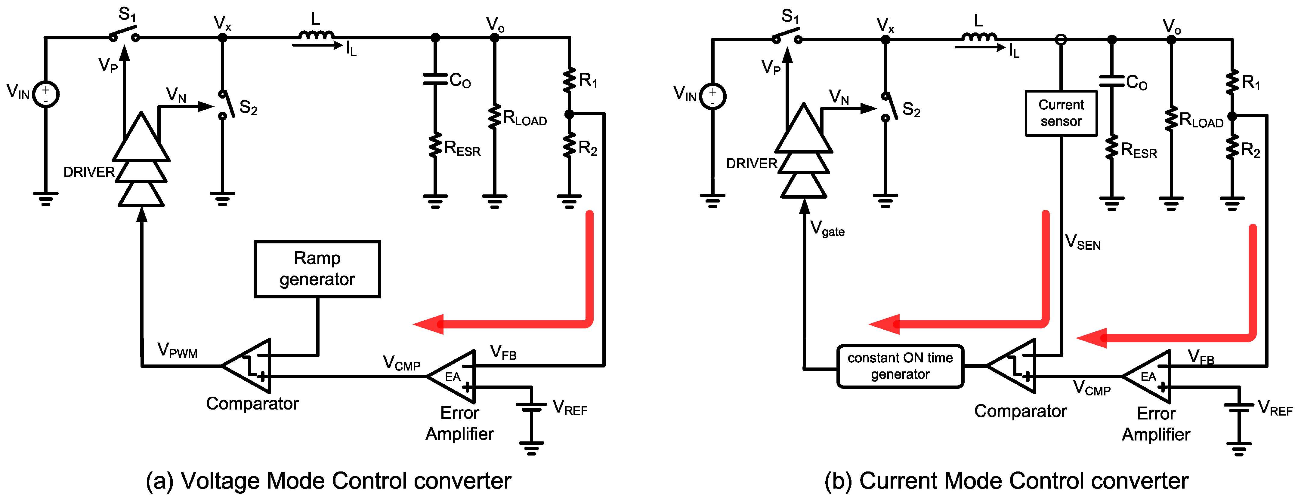
In the existing control schemes of the buck converter, it can be roughly divided into two control modes: voltage mode control (VMC) [11] and current mode control (CMC) [12,13,14,15]. Figure 1 shows the structures of these control modes. From Figure 1, we can find that the difference between the two modes lies in the feedback path. Since the CMC has more of a feedback path than the VMC, the CMC should give a good performance in regard to the transient response and the voltage regulation. Therefore, the CMC technology is widely used in power conversion technology.
Similar to the VMC buck converter, the converter structure based on the charge pumps has been proposed in [16]. The charge-pump-based converter [16] is very suitable in a boost topology. The main advantage of the [16] is that the converter can be fully integrated into silicon. Therefore, the literature [16] provides a good solution for ultra-low power applications. On the other side, similar to the CMC buck converter, Ballo et al. [17] proposed a novel scheme to improve charge transfer switches in linear charge pumps. The proposed converter in [17] belongs to the SC type.
In the switched inductor-based converters, there are many types of the CMC, including peak current mode (PCM), average current mode (ACM), constant on/off time, and adaptive on time (AOT) [18,19,20,21,22,23,24,25,26,27,28,29]. The feature of the CMC is that it needs to directly or indirectly sense the information of inductor current. Therefore, many works of the literature discuss how to sense the inductor current. These works in the literature are summarized and analyzed in [30].
This paper presents a no-inductor-current-sensor buck converter, which adopts dual loops control mechanism. At the same time, the proposed converter has the feature of a constant switching frequency.
2. Proposed Control Topology and Circuit Realization
2.1. Proposed Control Topology
Figure 2 shows the proposed control topology. It uses the dual controllers to regulate the output voltage and the switching frequency. The “proposed adaptive TOFF controller” keeps the switching frequency constant, and the “proposed adaptive TON controller” regulates the output voltage. This topology does not require a current sensor to detect the inductor current actually. The states of switches S1 and S2 are non-overlapping and complementary.
The subfunction blocks in Figure 2 are described as follows:
- (A)
- Constant Frequency Mechanism:
The work of this module is mainly used to detect the switching frequency of the system and generate a control voltage to send to the “proposed adaptive TOFF controller” module. The control signal can adjust TOFF to make the switching frequency constant.
- (B)
- Proposed adaptive TOFF controller:
The work of this module is mainly to regulate TOFF. This module controls the TOFF by the signal of the “constant frequency mechanism”.
- (C)
- Proposed adaptive TON controller:
The work of this module is mainly to regulate TON. This module function is similar to the “proposed adaptive TOFF controller”. This module controls the TON by the output signal of the EA.
- (D)
- EA (Error Amplifier)
The work of the EA is mainly to regulate VFB to VREF, that is, the VFB is equal to the VREF. Because the relationship between Vo and VFB is a resistor division in Figure 3, the Vo value can be decided by setting VREF.
- (E)
- DRIVER:
The work of the DRIVER is mainly to generate sufficient driving capability to drive the switches S1 and S2.
The advantages and disadvantages, as compared with the conventional schemes are listed below:
- Advantages
- (A)
- The scheme does not need to design a complex sensing circuit to sense the inductor current at any time. Compared with the scheme of using the current sensor [2], the proposed scheme is easy to implement and suitable for mass production.
- (B)
- The whole control circuit does not require special semiconductor devices, and there is no special matching issue in layout.
- (C)
- By the “constant frequency mechanism” module, the proposed scheme can make the switching frequency constant, which greatly reduces the difficulty in solving EMI issue. Moreover, the “constant frequency mechanism” is easy to implement, instead of PLL [31].
- Disadvantages
- (A)
- In contrast to SC converter, the scheme cannot be fully integrated into silicon.
2.2. Circuit Realization and Operating Principle
The implementation of the proposed converter is shown in Figure 3. From Figure 3, the realization of the controllers is effortless and suitable for PMIC. In addition, the “constant frequency mechanism” module is realized by referring [31]. For different applications, VO can be designed to the required value by adjusting the VREF in Figure 3. Furthermore, the switching frequency of the converter can also be adjusted by VREF2. Therefore, such a scheme is very flexible in the design. The operation of the converter in Figure 3 can be listed as follows:
- The switch S1 turns ON, and the switch S2 turns OFF. In this state, the inductor is in the charging phase. The ON time of S1 is labeled as TON. The TON is determined by the “proposed adaptive TON controller” module. When S1 is ON, the Vramp begins to rise toward the VCMP. Once the Vramp reaches the VCMP, the S1 is turned OFF, and the S2 is turned ON.
- The switch S1 turns OFF, and the switch S2 turns ON. In this state, the inductor is in the discharging phase. The OFF time of S1 is labeled as TOFF. The TOFF is determined by the “proposed adaptive TOFF controller” module.
- The “constant frequency mechanism” works to detect the switching frequency. The VEA1 controls the “proposed adaptive TOFF controller” to decide TOFF [31].
- In the steady state, the VFB and the Vfreq are almost equal to the VREF and the VREF2, respectively. In other words, the VCMP and the VEA1 will eventually converge to their stable voltages. The key waveforms of the converter are drawn in Figure 4.
3. Theoretical Analysis
3.1. Mathematical Model
As in [30,31], to verify the system’s stability, a mathematical model must be built. Since the converter can be regarded as an analog/digital hybrid system, it is not easy to establish a mathematical model accurately. Much relevant research about modeling is discussed in [32,33,34,35]. Ridley et al. [35] is the most popular reference in the literature. The purpose of mathematical modeling is to help obtain design parameters and increase the reliability of the designed circuit.
By referring to [35], the open-loop transfer function of the converter can be expressed as Equation (1). In Equation (2), the GP(s) is the transfer function of the buck converter. The transfer function of the “EA” module is represented as A(s), composed of the transconductance, gm, and the compensation network. Figure 5 illustrates these relationships.
Figure 5 is derived from Figure 3. In order to measure the open-loop response, the line labeled VCMP in Figure 3 must be broken. In Figure 5, the “constant frequency mechanism” and the “proposed adaptive TOFF controller” modules can be mapped to Figure 3. The “proposed adaptive TON controller” of Figure 5 is divided into three parts: (a) comparator, (b) digital logic, and (c) TON ramp generator, which can also be mapped to Figure 3.
where is the gain of the TON ramp generator, , and
From Equations (1)–(3), it can be seen that the values of the Ki, RO, R3 and C1 will affect the performance of the converter. Generally, the zero wz of the A(s) is designed to be equal to the output pole of the buck converter, as shown in Equation (4). Considering the stability, the pole wp location of the A(s) is designed to be let the system stable. Chou et al. [30,31] introduced the detailed design procedure for this type of the converter and verified it by using MathCAD and SIMPLIS.
Briefly, the C1, RO and R3 are the key design parameters which mainly affect the frequency compensation. In Figure 3, if the external components are confirmed, the Co, RESR, RLOAD and L can be the fixed values. The designer must carefully select the remaining components, especially C1, RO and R3.
3.2. Component Selection
4. Simulation Results
4.1. SIMPLIS Schematic
The SIMPLIS schematic of the proposed converter was built and is shown in Figure 6. For well mapping to Figure 3, the SIMPLIS schematic is grouped by the function module, and annotated on it. For example, the “Constant Frequency Mechanism”, “Proposed Adaptive TON Controller”, “Proposed Adaptive TOFF Controller,” and “DRIVER” modules are all clearly illustrated and annotated in Figure 6.
4.2. Transient Performance
Figure 7 shows the load transient response of the proposed converter. Similar to [30,31], the load current is changed between 0.1 and 0.5 A. The input/output voltages are set to 3.3 V/1.8 V. The recovery time is defined as when the load changes, and the output voltage recovers to within 1% of 1.8 V.
In Figure 7, the step-up and step-down recovery times of the load current transition are 1.5 μs and 0.9 μs, respectively. Therefore, the recovery time of the proposed converter is less than 1.5 μs. In addition, the specifications of the overshoot and undershoot voltage are measured as 16 mV and 12 mV, respectively, both within the range of 16 mV.
The converter can work under the Vin of 3.6 V–3.0 V, and the output voltage is 1.0 V–2.5 V. Figure 8 shows that the maximum ripple voltage is 2.7 mV when the Vin is 3.6 V, the Vo is 2.5 V and load current is 500 mA.
4.3. Load Regulation
The load regulation follows Equation (5). This specification indicates the output regulation capability when the load changes. In application, the load regulation should be as small as possible. Similar to [30,31], the simulation conditions are set as follows: The input/output voltages are 3.3 V/1.8 V. The load current varies from 0.5 A to 0.1 A. As shown in Figure 9, the load regulation is 0.04% through Equation (5).
where is the voltage at the 0.5 A load current, and is the 0.1 A load current.
4.4. Line Regulation
The line regulation follows Equation (6). This specification indicates the output regulation capability when the supply voltage changes. In application, the line regulation should be as small as possible. In the simulation, the supply voltage ranges from 3.0 V to 3.6 V. However, through Equation (6), we can see that the value of this specification is close to 0. Obviously, this specification cannot be presented in the system-level simulation. In general, the real situation may be worse than the simulation.
where ΔVin is the variation of the input voltage, and ΔVo is the variation of the output voltage.
4.5. Switching Frequency Regulation
By the constant frequency mechanism, the adaptive TOFF controller makes the switching frequency constant. The work of the constant switching frequency is summarized as follows: (Figure 3)
- (A)
- Conversion step:
It converts the information of switching frequency into an analog voltage, Vfreq, as shown in Figure 3.
- (B)
- Regulation step:
It uses the error amplifier (EA) to regulate the Vfreq to the designed value, VREF2. The output voltage of the error amplifier will decide the TOFF, that is, the switching frequency.
4.6. Performance List
The performance of the novel buck converter is summarized in Table 2. From the 100 mA load current to the 500 mA load current, the recovery time is less than 1.5 μs. Furthermore, the converter gives a good performance under a supply voltage of 3.0 V–3.6 V and an output voltage of 1.8 V. Finally, the performance comparisons with reported converters are listed in Table 3.
5. Conclusions
In this paper, a novel buck converter with a dual-loop control mechanism is proposed. The converter adopts a novel method to generate the TON and TOFF. The converter has three advantages. First, the control scheme does not need a current sensor, thus greatly reducing the circuit complexity, and it is suitable for mass production. Second, the proposed scheme can make the switching frequency constant, which greatly reduces the difficulty in solving EMI issue. Third, the whole circuit does not require special semiconductor devices to implement, and there is no special matching issue in layout. The scheme was verified by using SIMPLIS. The simulation results show that this control topology can still obtain a good performance, without realizing the inductor current sensor. Furthermore, the proposed buck converter can be implemented with TSMC 0.35 μm 2P4M CMOS processes.
Author Contributions
Conceptualization, H.-H.C. and S.-F.W.; Formal analysis, H.-H.C. and W.-H.L.; Methodology, H.-H.C.; Validation, H.-H.C. and W.-H.L.; Writing—original draft, H.-H.C.; Writing—review & editing, H.-H.C. and H.-L.C. All authors have read and agreed to the published version of the manuscript.
Funding
This research was funded by Ministry of Science and Technology, Taiwan, under Grants MOST 110-2222-E-346-001.
Conflicts of Interest
The authors declare no conflict of interest.
References
- Chen, J.-J.; Lu, M.-X.; Wu, T.-H.; Hwang, Y.-S. Sub-1-V Fast-Response Hysteresis-Controlled CMOS Buck Converter Using Adaptive Ramp Techniques. IEEE Trans. Very Large Scale Integr. (VLSI) Syst. 2012, 21, 1608–1618. [Google Scholar] [CrossRef]
- Chen, J.-J.; Hwang, Y.-S.; Chen, J.-H.; Ku, Y.-T.; Yu, C.-C. A New Fast-Response Current-Mode Buck Converter with Improved I2 -Controlled Techniques. IEEE Trans. Very Large Scale Integr. (VLSI) Syst. 2018, 26, 903–911. [Google Scholar] [CrossRef]
- Hwang, Y.S.; Chen, J.J.; Ku, Y.T.; Yang, J.Y. An Improved Optimum-Damping Current-Mode Buck Converter with Fast-Transient Response and Small-Transient Voltage using New Current Sensing Circuits. IEEE Trans. Ind. Electron. 2020, 68, 9505–9514. [Google Scholar] [CrossRef]
- Ballo, A.; Grasso, A.D.; Palumbo, G. A Review of Charge Pump Topologies for the Power Management of IoT Nodes. Electronics 2019, 8, 480. [Google Scholar] [CrossRef] [Green Version]
- Ballo, A.; Grasso, A.D.; Palumbo, G.; Tanzawa, T. Charge Pumps for Ultra-Low-Power Applications: Analysis, Design, and New Solutions. IEEE Trans. Circuits Syst. II 2021, 68, 2895–2901. [Google Scholar] [CrossRef]
- Souza, A.F.; Tofoli, F.L.; Ribeiro, E.R. Switched Capacitor DC-DC Converters: A Survey on the Main Topologies, Design Characteristics, and Applications. Energies 2021, 14, 2231. [Google Scholar] [CrossRef]
- Seeman, M.D.; Sanders, S.R. Analysis and Optimization of Switched-Capacitor DC–DC Converters. IEEE Trans. Power Electron. 2008, 23, 841–851. [Google Scholar] [CrossRef]
- Deepa, K.; Saju, H.; Kumar, M. Soft switched flyback converter for smps applications. In Proceedings of the 2013 International Conference on Control Communication and Computing (ICCC), Thiruvananthapuram, India, 13–15 December 2013; pp. 475–478. [Google Scholar]
- Aharon, I.; Kuperman, A.; Aharon, I.; Shmilovitz, D. Analysis of Bi-Directional Buck-Boost Converter for Energy Storage Applications. In Proceedings of the IECON 2013—39th Annual Conference of the IEEE Industrial Electronics Society, Vienna, Austria, 10–13 November 2013; pp. 88–96. [Google Scholar]
- Gallo, C.A.; Tofoli, F.L.; Pinto, J.A.C. Two-Stage Isolated Switch-Mode Power Supply with High Efficiency and High Input Power Factor. IEEE Trans. Ind. Electron. 2010, 57, 3754–3766. [Google Scholar] [CrossRef]
- Huang, Q.; Zhan, C.; Burm, J. A 30-MHz Voltage-Mode Buck Converter Using Delay-Line-Based PWM Control. IEEE Trans. Circuits Syst. II Express Briefs 2018, 65, 1659–1663. [Google Scholar] [CrossRef]
- Chen, J.-J.; Hwang, Y.-S.; Ku, Y.-T.; Li, Y.-H.; Chen, J.-A. A Current-Mode-Hysteretic Buck Converter with Constant-Frequency-Controlled and New Active-Current-Sensing Techniques. IEEE Trans. Power Electron. 2020, 36, 3126–3134. [Google Scholar] [CrossRef]
- Chen, J.-J.; Hwang, Y.-S.; Lin, J.-Y.; Ku, Y. A Dead-Beat-Controlled Fast-Transient-Response Buck Converter with Active Pseudo-Current-Sensing Techniques. IEEE Trans. Very Large Scale Integr. (VLSI) Syst. 2019, 27, 1751–1759. [Google Scholar] [CrossRef]
- Chen, W.-W.; Chen, J.-F.; Liang, T.-J.; Wei, L.-C.; Ting, W.-Y. Designing a Dynamic Ramp with an Invariant Inductor in Current-Mode Control for an On-Chip Buck Converter. IEEE Trans. Power Electron. 2013, 29, 750–758. [Google Scholar] [CrossRef]
- Saini, D.K.; Reatti, A.; Kazimierczuk, M.K. Average Current-Mode Control of Buck DC-DC Converter with Reduced Control Voltage Ripple. In Proceedings of the 42nd Annual Conference of the IEEE Industrial Electronics Society, Florence, Italy, 23–26 October 2016; IECON: Florence, Italy, 2016. [Google Scholar]
- Ballo, A.; Bottaro, M.; Grasso, A.D.; Palumbo, G.; Grasso, A.D. Regulated Charge Pumps: A Comparative Study by Means of Verilog-AMS. Electronics 2020, 9, 998. [Google Scholar] [CrossRef]
- ABallo, A.; Grasso, A.D.; Palumbo, G. Current-mode body-biased switch to increase performance of linear charge pumps. Int. J. Circuit Theory Appl. 2020, 48, 1864–1872. [Google Scholar]
- Yan, Y.; Lee, F.C.; Mattavelli, P.; Liu, P.-H. I2 Average Current Mode Control for Switching Converters. IEEE Trans. Power Electron. 2013, 29, 2027–2036. [Google Scholar] [CrossRef]
- Redl, R.; Sokal, N.O. Current-mode control, five different types, used with the three basic classes of power converters: Small-signal AC and large-signal DC characterization, stability requirements, and implementation of practical circuits. In Proceedings of the 1985 IEEE Power Electronics Specialists Conference, Toulouse, France, 24–28 June 1985; pp. 771–785. [Google Scholar]
- Li, J. Current-Mode Control: Modeling and its Digital Application. Ph.D. Dissertation, Faculty of the Virginia Polytechnic Institute and State University, Blacksburg, VA, USA, 2009. [Google Scholar]
- Zhong, S.; Shen, Z. A Hybrid Constant On-Time Mode for Buck Circuits. Electronics 2021, 10, 930. [Google Scholar] [CrossRef]
- Lin, Y.-C.; Chen, C.-J.; Chen, D.; Wang, B. A Ripple-Based Constant On-Time Control with Virtual Inductor Current and Offset Cancellation for DC Power Converters. IEEE Trans. Power Electron. 2012, 27, 4301–4310. [Google Scholar] [CrossRef]
- Nien, C.-F.; Chen, D.; Hsiao, S.-F.; Kong, L.; Chen, C.-J.; Chan, W.-H.; Lin, Y.-L. A Novel Adaptive Quasi-Constant On-Time Current-Mode Buck Converter. IEEE Trans. Power Electron. 2016, 32, 8124–8133. [Google Scholar] [CrossRef]
- Lin, H.-C.; Fung, B.-C.; Chang, T.-Y. A current mode adaptive on-time control scheme for fast transient DC-DC converters. In Proceedings of the 2008 IEEE International Symposium on Circuits and Systems, Seattle, WA, USA, 18–21 May 2008; pp. 2602–2605. [Google Scholar]
- Zhen, S. Variable on time controlled buck converter for DVS applications. In Proceedings of the Conference of the IEEE Industrial Electronics Society, Beijing, China, 29 October–1 November 2017; pp. 1642–1648. [Google Scholar]
- Bari, S.; Li, Q.; Lee, F.C. Fast Adaptive on Time Control for Transient Performance Improvement. In Proceedings of the 2015 IEEE Applied Power Electronics Conference and Exposition (APEC), Charlotte, NC, USA, 15–19 March 2015; pp. 397–403. [Google Scholar]
- Liu, P.-J.; Kuo, M.-H. Adaptive On-Time Buck Converter with Wave Tracking Reference Control for Output Regulation Accuracy. Energies 2021, 14, 3809. [Google Scholar] [CrossRef]
- Bari, S.; Li, Q.; Lee, F.C. A New Fast Adaptive On-Time Control for Transient Response Improvement in Constant On-Time Control. IEEE Trans. Power Electron. 2018, 33, 2680–2689. [Google Scholar] [CrossRef]
- Wong, L.K.; Man, T.K. Adaptive On-Time Converters. IEEE Ind. Electron. Mag. 2010, 4, 28–35. [Google Scholar] [CrossRef]
- Chou, H.-H.; Chen, H.-L.; Fan, Y.-H.; Wang, S.-F. Adaptive On-Time Control Buck Converter with a Novel Virtual Inductor Current Circuit. Electronics 2021, 10, 2143. [Google Scholar] [CrossRef]
- Chou, H.-H.; Chen, H.-L. A Novel Buck Converter with Constant Frequency Controlled Technique. Energies 2021, 14, 5911. [Google Scholar] [CrossRef]
- Li, J.; Lee, F.C. New modeling approach and equivalent circuit representation for current-mode control. IEEE Trans. Power Electron. 2010, 25, 1218–1230. [Google Scholar]
- Enrique, J.M.; Barragán, A.J.; Durán, E.; Andújar, J.M.; Gómez, J.M.E.; Piña, A.J.B.; Aranda, E.D.; Márquez, J.M.A. Theoretical Assessment of DC/DC Power Converters’ Basic Topologies. A Common Static Model. Appl. Sci. 2017, 8, 19. [Google Scholar] [CrossRef] [Green Version]
- Suntio, T. Dynamic Modeling and Analysis of PCM-Controlled DCM-Operating Buck Converters—A Reexamination. Energies 2018, 11, 1267. [Google Scholar] [CrossRef] [Green Version]
- Ridley, R.B. An Accurate and Practical Small-Signal Model for Current-Mode Control. Available online: www.ridleyengineering.com (accessed on 24 July 2021).
- Zhen, S.; Zeng, P.; Chen, J.; Zhou, W.; Wang, J.; Luo, P.; Zhang, B. Transient Response Improvement of DC-DC Converter by Current Mode Variable on Time Control. In Proceedings of the 2018 IEEE 61st International Midwest Symposium on Circuits and Systems (MWSCAS), Windsor, ON, Canada, 5–8 August 2018. [Google Scholar]
- Jiang, C.R.; Chai, C.C.; Han, C.X.; Yang, Y.T. A high performance adaptive on-time controlled valley-current-mode DCDC buck converter. J. Semicond. 2020, 41, 062406. [Google Scholar] [CrossRef]
Figure 1.
The control topology of the conventional converter.

Figure 2.
Control topology of the proposed converter.

Figure 3.
Implementation of the proposed converter.
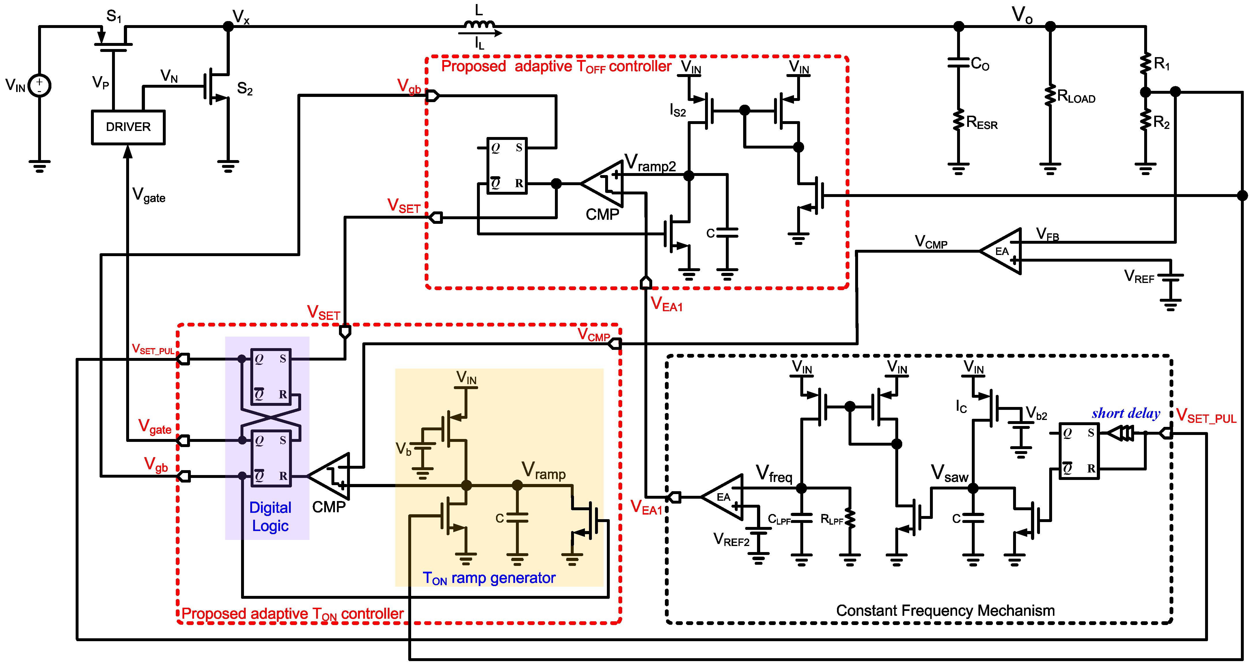
Figure 4.
Key waveforms of the proposed converter.
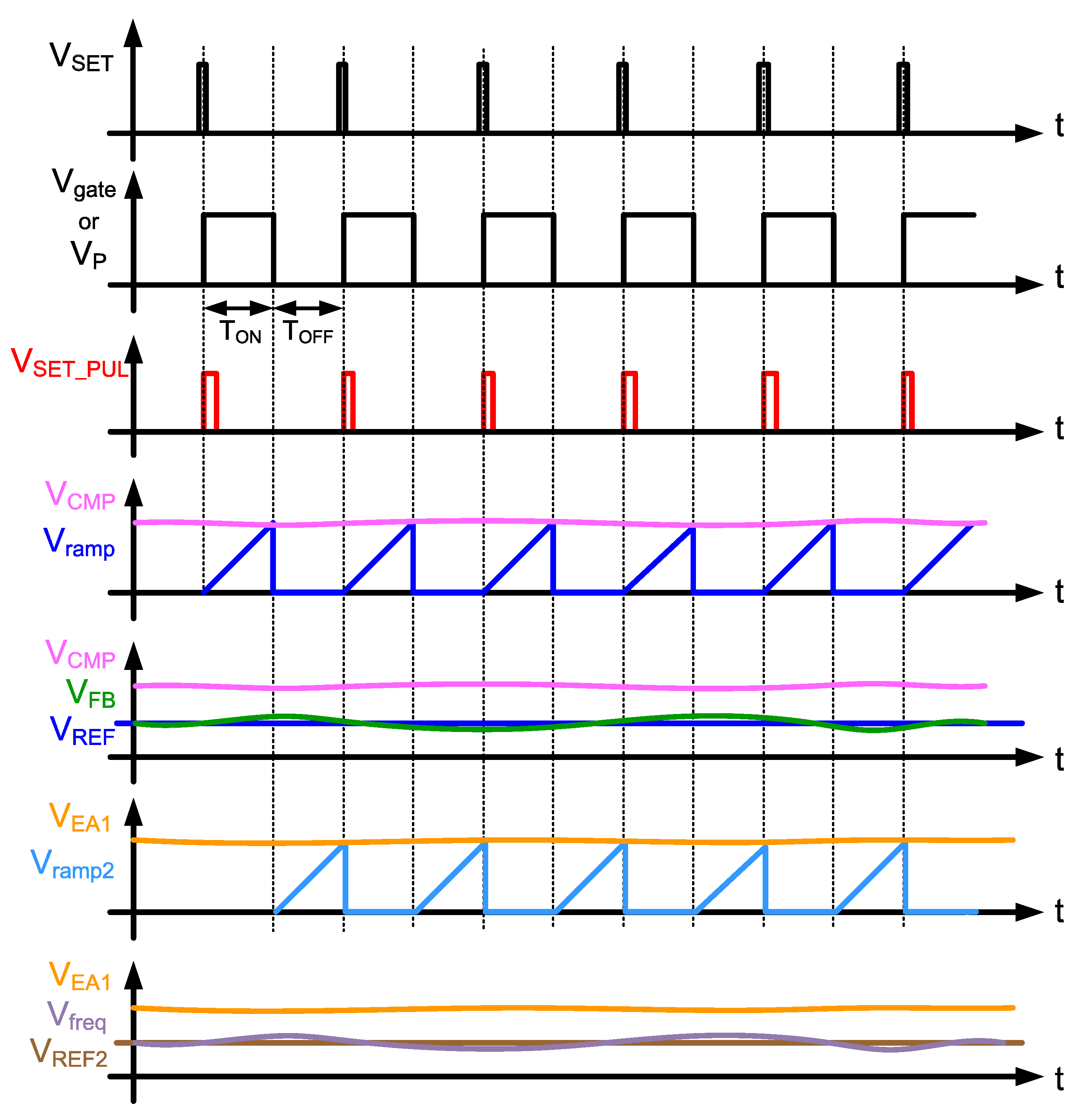
Figure 5.
Block diagram of the overall transfer function.
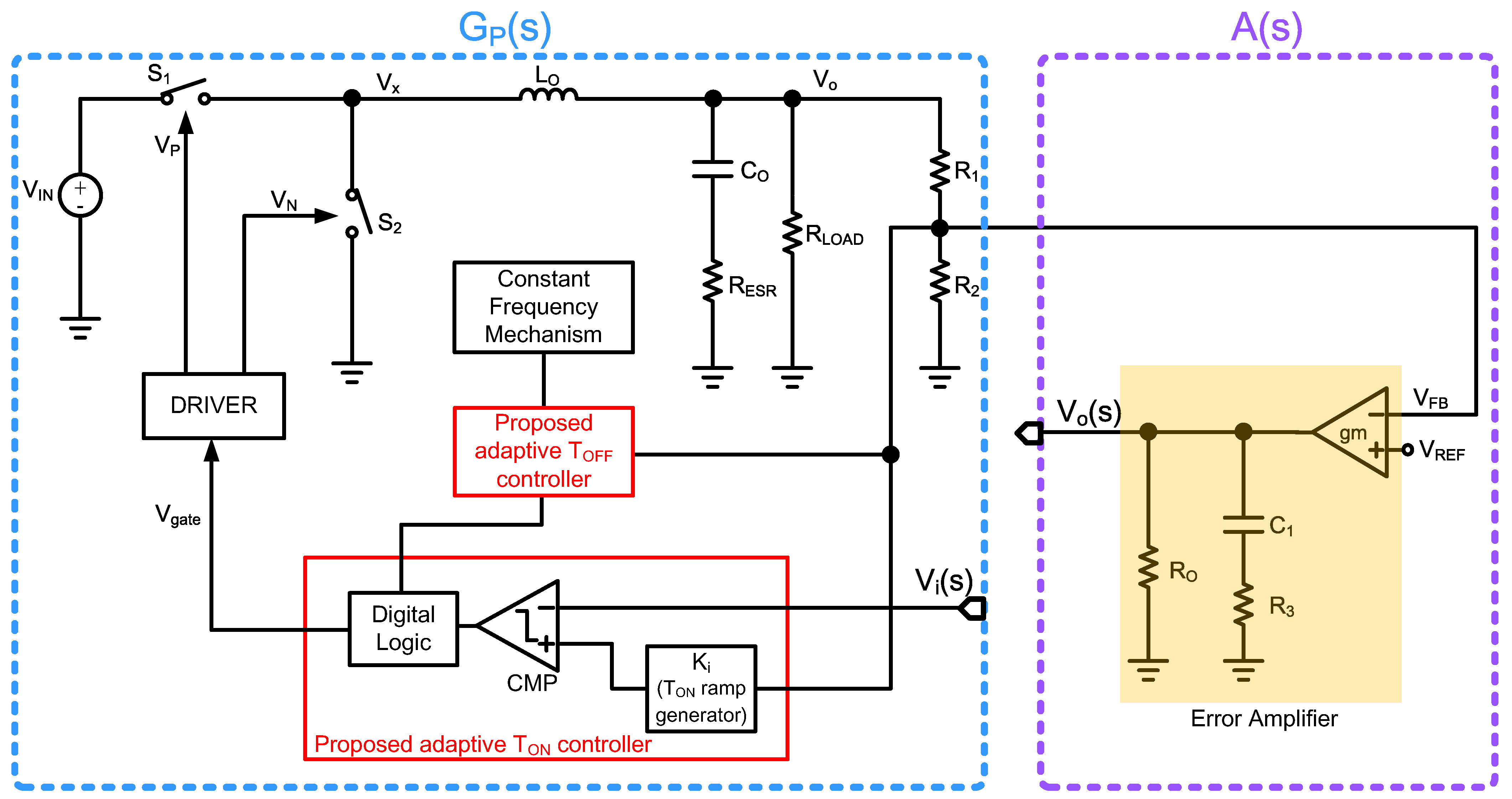
Figure 6.
Schematic of the proposed converter.

Figure 7.
The recovery times for load current transition between 100–500 mA. (a) step-up. (b) step-down.
Figure 7.
The recovery times for load current transition between 100–500 mA. (a) step-up. (b) step-down.
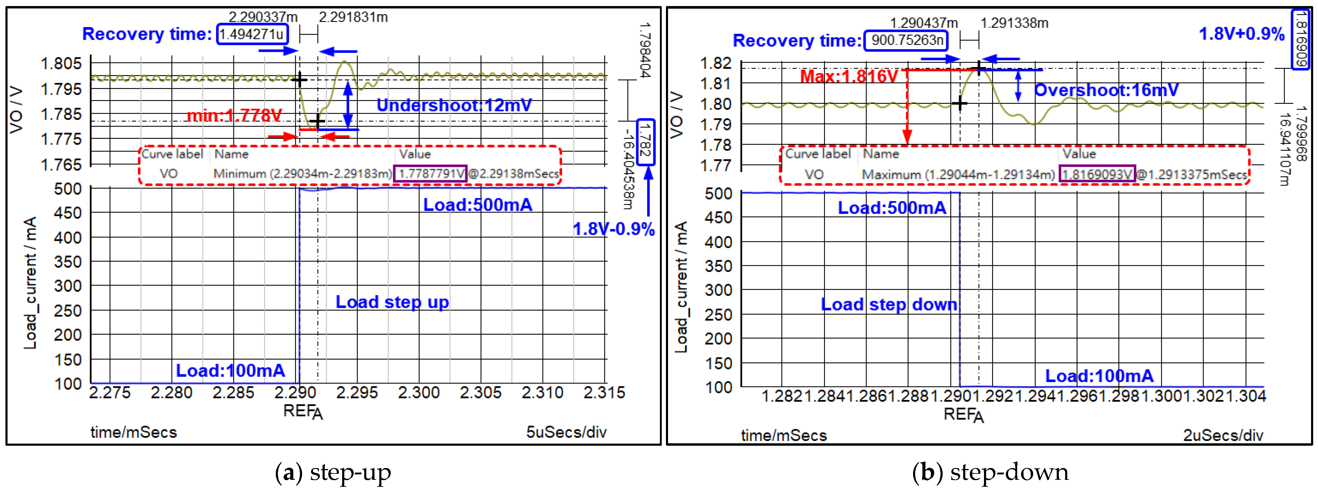
Figure 8.
Performance over a wide input range.
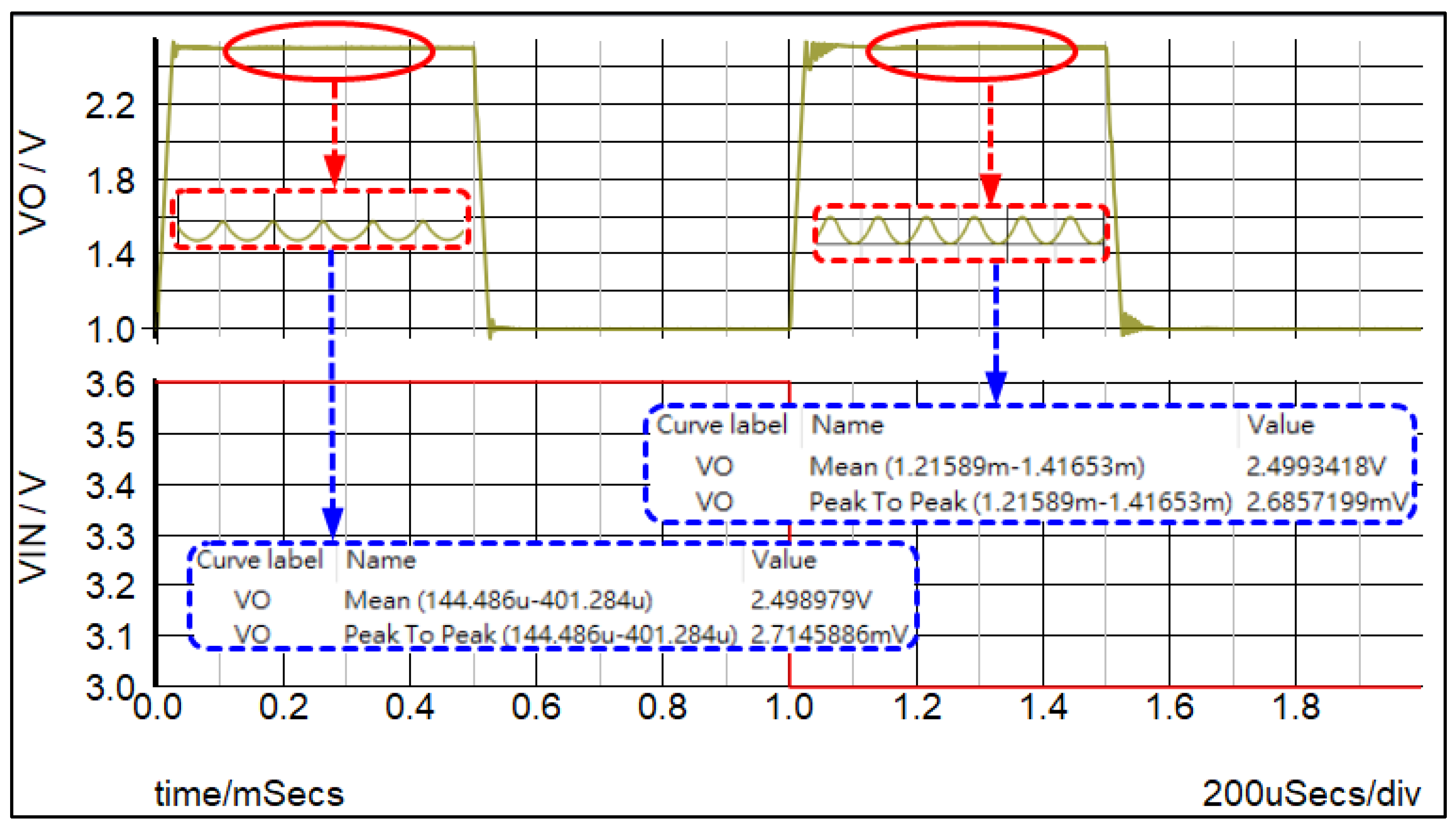
Figure 9.
Load regulation.

Figure 10.
The switching frequency results.


Table 1.
Design parameters.
| Component | Value | Unit |
|---|---|---|
| RLOAD | 3.6 | Ω |
| Co | 10 | μF |
| L | 4.7 | μH |
| RESR | 5 | mΩ |
| Ro | 1 | MΩ |
| R3 | 180 | kΩ |
| C1 | 200 | pF |
Table 2.
Performance summary.
| Parameter | Conditions | Min. | Typ. | Max. | Unit |
|---|---|---|---|---|---|
| Input voltage | 3.0 | 3.6 | V | ||
| Output voltage | 1.0 | 2.5 | V | ||
| Output ripple | Vin = 3.6 V, Vo = 2.5 V | 2.7 | mV | ||
| Load current | 100 | 500 | mA | ||
| Inductor | DCR *: 30 mΩ | 4.7 | μH | ||
| Output capacitor | ESR: 5 mΩ | 10 | μF | ||
| Switching frequency | Vin = 3.0~3.6 V, Vo = 1.0~2.5 V | 1 | MHz | ||
| Recovery time (step-up) | Vo = 1.8 V Load current: 100 mA to 500 mA | 1.5 | μs | ||
| Recovery time (step-down) | Vo = 1.8 V Load current: 500 mA to 100 mA | 0.9 | μs | ||
| Overshoot voltage | Vin = 3.3 V, Vo = 1.8 V | 16 | mV | ||
| Undershoot voltage | Vin = 3.3 V, Vo = 1.8 V | 12 | mV |
* DCR: the DC resistance of inductor.
Table 3.
Performance comparisons with reported converters.
| References | 2018 [36] | 2020 [37] | 2021 [30] | 2021 [31] | This Work |
|---|---|---|---|---|---|
| Results | simulation | simulation | simulation | simulation | simulation |
| Control scheme | AOT | AOT | AOT | AOT | dual loops |
| Process (μm) | 0.35 | 0.18 | 0.35 ** | 0.18 ** | 0.35 ** |
| Input voltage (V) | 12 | 3.3–5.0 | 3.0–3.6 | 3.0–3.6 | 3.0–3.6 |
| Output voltage (V) | 1.2 | 1.8 | 1.0–2.5 | 1.0–2.5 | 1.0–2.5 |
| Inductor (μH) | 1 | 1.5 | 4.7 | 4.7 | 4.7 |
| Output Capacitor (μF) | 47 | 20 | 10 | 10 | 10 |
| Switching Frequency (MHz) | 1 | 1 | 1 | 1 | 1 |
| Switching frequency variation (%) | N/A | N/A | N/A | <1% | <1% |
| Max. Load current (mA) | 5000 | 2000 | 500 | 500 | 500 |
| Load current step (mA) | 4000 | 800 | 400 | 400 | 400 |
| Undershoot/Overshoot (mV) | 20/26 | 13/14 | 23/26 | 20/24 | 16/12 |
| Recovery time (μs) (rise/fall) | <3 | 6/2 | 1.98/1.6 | 1.69/1.62 | 1.5/0.9 |
** This work is system level simulation with SIMPLIS.
Publisher’s Note: MDPI stays neutral with regard to jurisdictional claims in published maps and institutional affiliations. |
© 2022 by the authors. Licensee MDPI, Basel, Switzerland. This article is an open access article distributed under the terms and conditions of the Creative Commons Attribution (CC BY) license (https://creativecommons.org/licenses/by/4.0/).
Share and Cite
MDPI and ACS Style
Chou, H.-H.; Luo, W.-H.; Chen, H.-L.; Wang, S.-F. A Novel Buck Converter with Dual Loops Control Mechanism. Electronics 2022, 11, 1256. https://doi.org/10.3390/electronics11081256
AMA Style
Chou H-H, Luo W-H, Chen H-L, Wang S-F. A Novel Buck Converter with Dual Loops Control Mechanism. Electronics. 2022; 11(8):1256. https://doi.org/10.3390/electronics11081256
Chicago/Turabian StyleChou, Hsiao-Hsing, Wen-Hao Luo, Hsin-Liang Chen, and San-Fu Wang. 2022. "A Novel Buck Converter with Dual Loops Control Mechanism" Electronics 11, no. 8: 1256. https://doi.org/10.3390/electronics11081256
Note that from the first issue of 2016, this journal uses article numbers instead of page numbers. See further details here.