
TID Sensitivity Assessment of Quadrature LC-Tank VCOs Implemented in 65-nm CMOS Technology


Department of Electrical Engineering (ESAT)-ADVISE, KU Leuven, 2440 Geel, Belgium
*
Author to whom correspondence should be addressed.
Electronics 2022, 11(9), 1399; https://doi.org/10.3390/electronics11091399
Submission received: 25 March 2022
/
Revised: 22 April 2022
/
Accepted: 26 April 2022
/
Published: 27 April 2022
(This article belongs to the Special Issue Radiation Tolerant Electronics, Volume II)
Abstract
:This article presents a comprehensive assessment of the ionizing radiation induced effects on the performance of quadrature phase LC-tank based voltage-controlled-oscillators (VCOs). Two different quadrature VCOs (QVCOs) that are capable of generating frequencies in the range of 2.5 GHz to 2.9 GHz are implemented in a commercial 65 nm bulk CMOS technology to target for harsh radiation environments like space applications and high-energy physics (HEP) experiments. Each of the QVCOs consumes 13 mW power from a 1.2 V supply. The architectures are based on the popular implementation of two different types of QVCOs: parallel-coupled QVCO (PQVCO) and super-harmonic coupled QVCO (SQVCO). The various performance metrics (oscillation frequency, quadrature phase, phase noise, frequency tuning range, and power consumption) of the two different QVCOs are evaluated with respect to a Total ionizing Dose (TID) up to a level of approximately 100 Mrad (SiO) through X-ray irradiation. During irradiation, the electrical characterization of the samples of the prototype are performed under biased condition at room temperature. Before irradiation, the QVCOs (PQVCO and SQVCO) achieve phase noise equal to −115 dBc/Hz and −119 dBc/Hz at 1 MHz offset, resulting in figure-of-merit (FoM) of −172.2 dBc/Hz and −176.4 dBc/Hz respectively. The test-setup of the TID experiment is discussed and the results obtained are statistically analyzed in this article to perform a comparative study of the performance of the two different QVCOs and evaluate the effectiveness of the radiation hardened by design techniques (RHBDs) employed in the implementations. Post-irradiation, the overall variations of the frequencies of the oscillators are less than 1% and the change in tuning range (TR) is less than 5% as observed from the tested samples.
Keywords:
quadrature; super-harmonic; LC-tank; Q-phase; VCO; QVCO; radiation; TID; SEE; X-ray; high energy physics; radiation hardened by design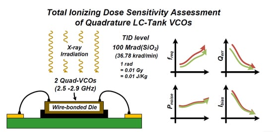
1. Introduction
Various high frequency designs predominantly in the area of radio-frequency and millimeter-wave based applications [1] require quadrature phase shifted signals to enable wireless as well as wired communication systems. Wireless communication systems with integrated transceivers require quadrature signals for up and down conversion and eventually require accurate quadrature phase for effective image-rejection in the base-band [2,3,4]. In the case of wired communication, QVCOs play a key role in multi-phase clock generation and in particular assist in the implementation of the half-rate clock and data recovery (CDR) circuits [5,6]. Additionally, QVCOs have also been explored to be integrated in phased-array transceivers [7,8].
Numerous integrated design techniques [9,10] for quadrature phase generation are reported in the literature to date and can be broadly identified as using (1) active R-C oscillators [11], (2) relaxation oscillators [12], (3) ring oscillators [13,14], (4) poly-phase filters [15,16], (5) frequency divide-by-2 circuits [17], (6) cross-coupled QVCOs, and (7) super-harmonic coupled QVCOs. Amid these, LC-tank oscillator-based options have prevailed as the design choice considering its superior performance in terms of phase noise and spectral purity within the given power budget. However, these are achieved with significant area penalty due to on-chip inductors. Other non-LC-tank based options are explored, despite the fact that, in some low-frequency applications they are limited by the area constraints and they do not have particularly stringent phase noise requirements. LC-tank based QVCOs typically contain two identical LC oscillators with the outputs cross coupled with each other. The quadrature outputs can be coupled through active devices [9,18,19,20] or passive devices [21,22]. The former method improves phase accuracy but at the cost of increased phase noise, whereas the latter showcases improved phase noise contribution but trades off phase accuracy due to limited coupling strength. Conventionally, the coupling mechanism in the cross-coupled QVCOs follow either parallel [9,20] or series [18] coupling schemes using the fundamental frequency component. The existing trade-off between phase noise and phase accuracy among these architectures can be eliminated by achieving quadrature phase locking using super-harmonic coupling, i.e., second harmonic injection at 180 out-of-phase at the oscillators’ common-mode nodes [10].
The use of QVCOs is extensive in various communication systems and half-rate CDR circuits. In modern days, these oscillators have also found indispensable use in high-speed communication in space (satellite communication, on-board spacefibre network) applications and data transmission during HEP experiments. Considering the harsh radiation environment these oscillators are subjected to, the oscillators required to sustain up to a TID level of several Mrad for space applications but several hundreds of Mrad for HEP experiment. In CMOS technology, the effects of radiation on metal–oxide–semiconductor field-effect transistor (MOSFET) devices are multifold. While exposed to continuous radiation, the performance of the devices is degraded with the change in threshold voltage, drain current, intrinsic gain and noise levels [23]. The radiation induced effects in presence of mismatch and non-linearity degenerate the system’s performance, and in many of the cases, striking radiation particles lead to functional failures and transients at the output. Radiation strike in the gate-oxide region of MOSFET devices generates pairs of electron–hole and its numbers are proportional to the energy deposited during the interaction and inversely proportional to the squared value of its gate-oxide thickness (). The oxide-trap charges result in an increase in threshold voltage for p-channel MOS (PMOS) devices and a decrease for n-channel MOS (NMOS) devices. This effect in NMOS devices is counter-acted by interface trap charges, but aggravated in the case of PMOS devices. With the scaling of CMOS technologies, the reduction in gate-oxide is likely to lessen the TID induced problems, but on the contrary has increased SEE induced transients due to the lower critical charge. However, in lower feature size (sub-90 nm) dense technologies, the accumulated charges in shallow trench isolation (STI) regions still affect the device performance [24,25,26] over the course of time.
As reported in the literature, the performance of LC-tank based single VCOs operating under ionizing radiation are extensively studied in [27,28]. The vulnerability of VCO architectures with respect to TID effects for space applications as well as in HEP experiments are explored in [29], whereas the effects of radiation-induced single-event-effects (SEEs) in VCOs are studied and a few possible remedies are suggested with some design improvements in [28,30,31]. In comparison, the knowledge about the effects of ionizing radiation on the performance of QVCOs are limited due to scarcity in the number of studies [32,33] done on QVCOs under radiation exposure. The SEE induced effects are studied in [32] on QVCOs implemented in 65 nm bulk CMOS technology. The TID induced effects on a parallel-coupled QVCO implemented in 32 nm silicon-on-insulator (SOI) CMOS technology is explored in [33]. The study reports on the degradation of several performance parameters (oscillation frequency, phase noise and power consumption), but gives no insight on the radiation induced effects on quadrature phase accuracy. This article focuses on giving more insights on the effects of radiation on QVCOs with a particular interest in TID induced variations. To the authors’ knowledge, for the first time to date, an experimental study and comparison of TID induced performance variation is done between two different topologies of LC-tank based QVCOs implemented in 65 nm bulk CMOS technology.
The rest of the article is arranged as follows: Section 2 discusses the implementation of the QVCOs in detail. The test-setup for X-ray irradiation is elaborated in Section 3 together with a detailed description of the results of the experiment and a comparison of performance studies of the two different QVCOs. Section 4 concludes the article with the summary of the TID sensitivity study on the two QVCOs.
2. Implementation
For the TID experiment, two different topologies of QVCOs are implemented for quadrature phase generation: parallel coupled QVCO (PQVCO) and super-harmonic coupled QVCO (SQVCO).
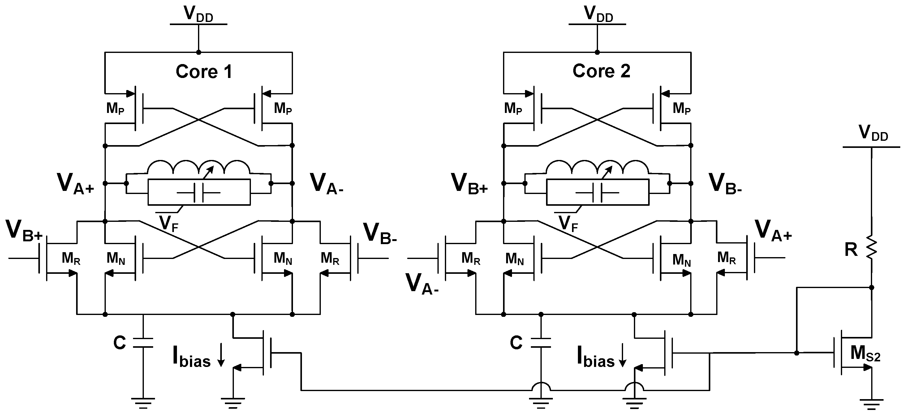
A schematic diagram of the PQVCO as proposed in [34] with two identical core structures is shown in Figure 1. Each oscillator core is implemented with complementary cross-coupled PMOS-NMOS transistor pairs () with an LC-tank. The output of each oscillator is coupled to the other’s output nodes parallelly using NMOS transistor () pairs. Based on theory explained in [35], if the two oscillator cores are symmetrical and matched in terms of parasitics, the four outputs , , , produce quadrature phase shifted differential In-phase and Q-phase (I and Q) output signals. The tunable capacitors in the LC-tank circuit are realised using n-well MOS varactors () and the inductor is implemented in top-metal to maximize the inductor quality factor. As shown in Figure 2a, the n-well MOS varactors are ac-coupled to the oscillator’s output nodes using capacitors (∼5 × ) and the gate-voltage is varied using connected through a resistor. This arrangement helps to reduce the sensitivity towards single event transients (SETs) [36]. Here, any charge collected between the n-well and p-substrate interface finds a low impedance path to ground through the metal wires. However, this improvement pays a penalty of reduced frequency tuning range (TR). Also wider devices are chosen for core PMOS-NMOS pairs () to minimize radiation induced performance variation [37], in particular to reduce parasitic turn-on of the lateral devices due to STI-trapped charges. However, the use of wider devices results in increased power consumption. The oscillators are designed to operate with full swing with large bias current (∼10 mA) at the edge of the current limited region to achieve optimum phase noise performance within the power budget. The bias current is generated by using typical current-mirror circuits formed with NMOS pairs. The bottom-biasing using NMOS is chosen instead of top-biased PMOS as the radiation induced variation is less in NMOS devices compared to PMOS devices in 65 nm CMOS technology [37].
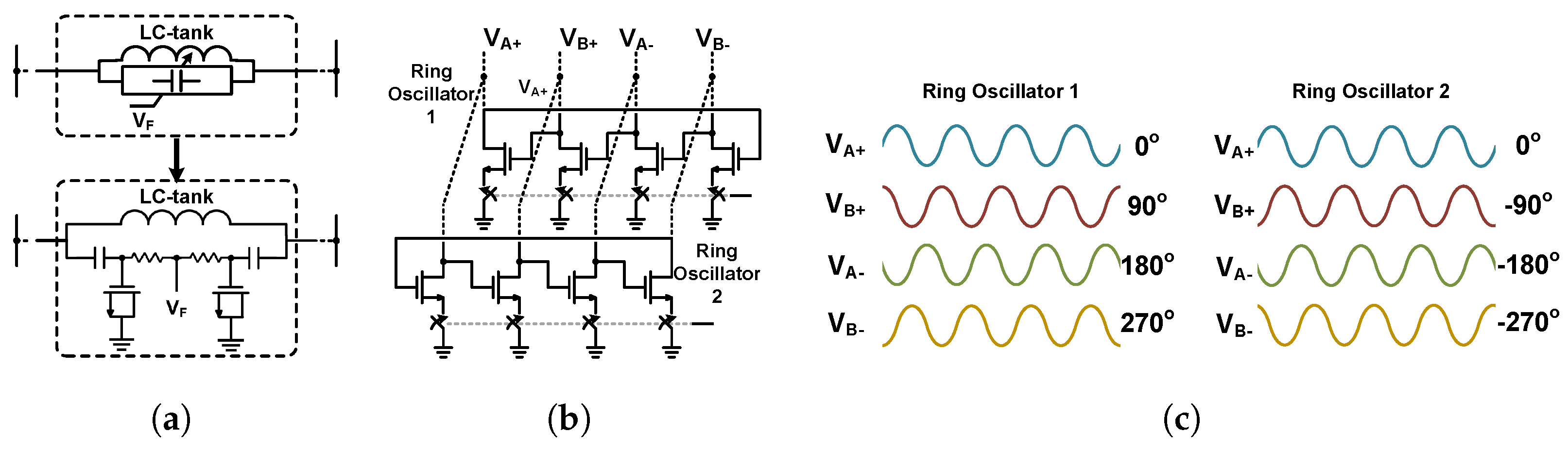
A simplified block diagram of the PQVCO cross-coupled with each other through transconductance () formed by the coupling NMOS transistors () is shown in Figure 3. The LC-tank circuits () form the tank band-pass filter at the resonance frequency and complementary PMOS-NMOS pairs () create the cell to compensate for tank losses. Quadrature phase accuracy can be improved with stronger coupling strength , but it leads to increased phase noise around the oscillation frequency. Therefore, the sizes of are chosen smaller (1/4 times) with respect to the core MOS devices () to minimize the phase noise contribution while maintaining the quadrature phase error within acceptable limits (<1). Due to symmetry in operation in the identical core structures, the PQVCO is likely to exhibit bi-modal oscillation [38]. But in presence of mismatch in the tank circuits or coupling devices one of the modes prevails and leads to oscillation with either 90 or −90 phase shifted outputs. The ambiguity in phase is resolved by introducing ring oscillator structures [2,39] at the output nodes. As shown in Figure 2b, two ring oscillators are provided and either of them can be enabled to direct the oscillation in either leading or lagging phases. The resulting waveforms of , , , based on different ring oscillator configurations are shown in Figure 2c.
Figure 4 shows a schematic of the SQVCO implemented for the TID experiment based on the architecture proposed in [39]. As elaborated in Figure 4, the two oscillator cores are identical in nature and the common-mode nodes are coupled with each other at 180 out-of-phase through a center-tap inductor. Ideally, in a differential configuration, the odd harmonics of the oscillator circulate through the switching core MOS devices, and higher order even harmonics appear at the common-mode node of the oscillator core. As per the super-harmonic injection locking mechanism [39], the second harmonics of each oscillator are mutually coupled with each other at 180 out-of-phase, and this leads to quadrature phase differences at the fundamental frequency component. Here, in this architecture a center-tap inductor is used in series with the bias circuit and each half is configured to resonate with the parasitic capacitors at twice the fundamental frequency. The second harmonic at the common-mode nodes are coupled magnetically through each half of the inductor and maintain a 180 phase difference between each other. A layout representation of the center-tap inductor working as the coupling transformer is shown in the bottom-left corner of Figure 4. The inductor is implemented in top-metal with dummy metal fillings and guard rings to prevent substrate coupling.
Unlike the PQVCOs, the absence of coupling through active devices in this architecture breaks the trade-off between quadrature accuracy and phase-noise contribution. Even though the sizes of the core MOS devices are identical in the PQVCO and SQVCO and both are driven by equal bias currents, the phase-noise performance is better in the SQVCO as compared to PQVCO. The coupling inductor acts as a tail-noise filter [40]. It generates a high impedance at twice the fundamental frequency at resonance and therefore reduces flicker noise up-conversion and thermal noise down-conversion around the oscillation frequency.
For better insights in the operation, a simplified block diagram of the SQVCO circuit components [2] are shown in Figure 5. The LC-tank components () act as a band-pass filter centered at resonance frequency where the tank losses are compensated by the cell created by the complementary PMOS-NMOS pairs (). The common-mode node at the oscillator core acts as frequency doubler and injects the signal to the other with an added phase shift of 180. The injected out-of-phase second harmonic produces a quadrature phase shift while mixing with the fundamental frequency component. Here, in this architecture the quadrature accuracy largely depends on the tail node impedance and resonating signal strength at the tail inductor [39]. Similar to the PQVCO, two ring oscillators are provided at the output nodes as shown in Figure 2b to resolve the quadrature phase ambiguity (lead or lag). In addition, the core PMOS-NMOS switching pairs and the bias circuit of both types of QVCOs: PQVCO and SQVCO, are implemented with p-type and n-type guard-rings to prevent single-event-latchup (SEL) induced failures.
The off-chip driving strength of the differential output signal pairs from the oscillators are improved using cascaded CMOS digital buffers with increased driving strength. As shown in Figure 6 Two parallel chains of digital buffers are used in differential configuration with cross-coupled latches connected in between the nodes for phase alignment.
3. Experimental Results
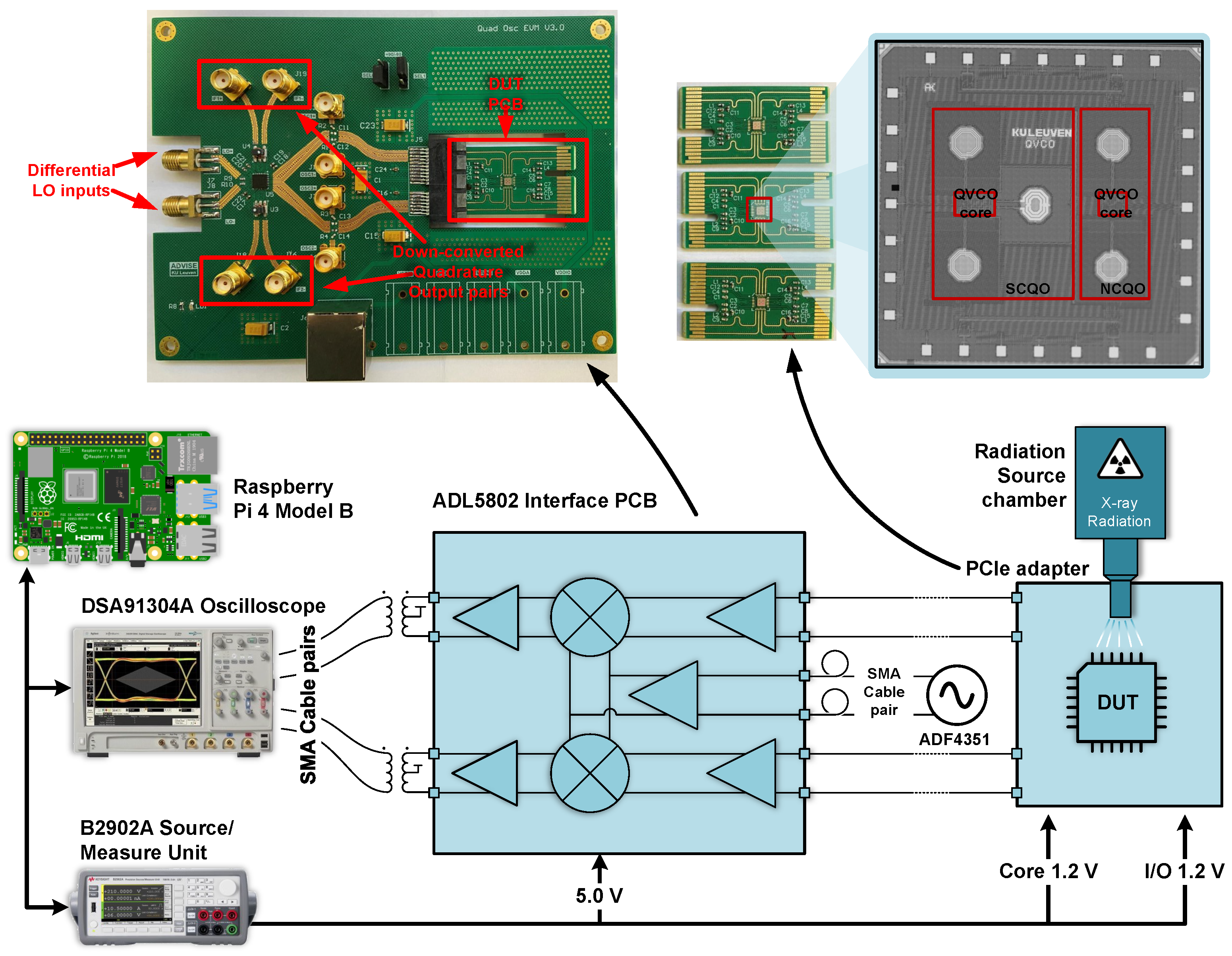
The prototypes of the quadrature LC oscillators (PQVCO and SQVCO) are implemented together in a single die using a commercial 9-metal 65 nm CMOS technology. An overview of the test setup used for the radiation assessment of the devices is provided in Figure 7. It consists of 2 printed-circuit-boards (PCBs) and the measurement equipment which are controlled by a raspberry pi 4 based controller board. The device-under-test (DUT) samples with the decoupling capacitors on the core and input-output () supplies are wire-bonded to peripheral-component-interconnect-express (PCIe) adapter boards. The micro-photograph of the fabricated die sample is shown in the top-right corner of Figure 7. The buffered quadrature outputs of the oscillators with an approximate frequency range of 2.5 GHz to 2.9 GHz are down-converted to an intermediate frequency (IF) of 500 MHz using an off-chip double balanced active mixer ADL5802. The DUT is connected to the mixer through the PCIe interface, and the mixer is driven by a differential local oscillator (LO) signal (2.4 GHz) generated from low phase noise VCO, ADF4351. The ADL5802 interface PCB with the DUT sample is placed inside the X-ray irradiation chamber. The differential IF quadrature output pairs from the on-board 1:1 balun transformer are brought out of the X-ray chamber to the Keysight DSA91304A oscilloscope using 2 m long sub-miniature version A (SMA) cables for frequency and quadrature phase measurement. The ADL5802 interface PCB and of the DUT are powered from a fixed 5 V and 1.2 V supplies respectively. One of the channels of the Keysight B2902A precision source/measure unit is used to provide 1.2 V to the and measure the current consumed. While the other channel is used to tune the varactor input voltage during the measurement. Additionally a PN9000 phase noise analyzer is utilized to measure the output phase noise of the free running quadrature oscillator.
The radiation assessment of the DUT is conducted under bias condition at room temperature. While testing, the DUT is placed at the center of the incident X-ray beam having a diameter of approximately 3 cm. The X-ray beam is generated from a 40 keV, 40 mA W-tube from Seifert and resulted in a dose rate of 36.78 krad/min. Before irradiation, the dose rate of the X-ray beam is calibrated using a PIN diode-based dose sensor. During irradiation, the various performance metrics (frequency, quadrature phase, core power) of the DUT are measured repeatedly up to a TID level of 100 Mrad (SiO).
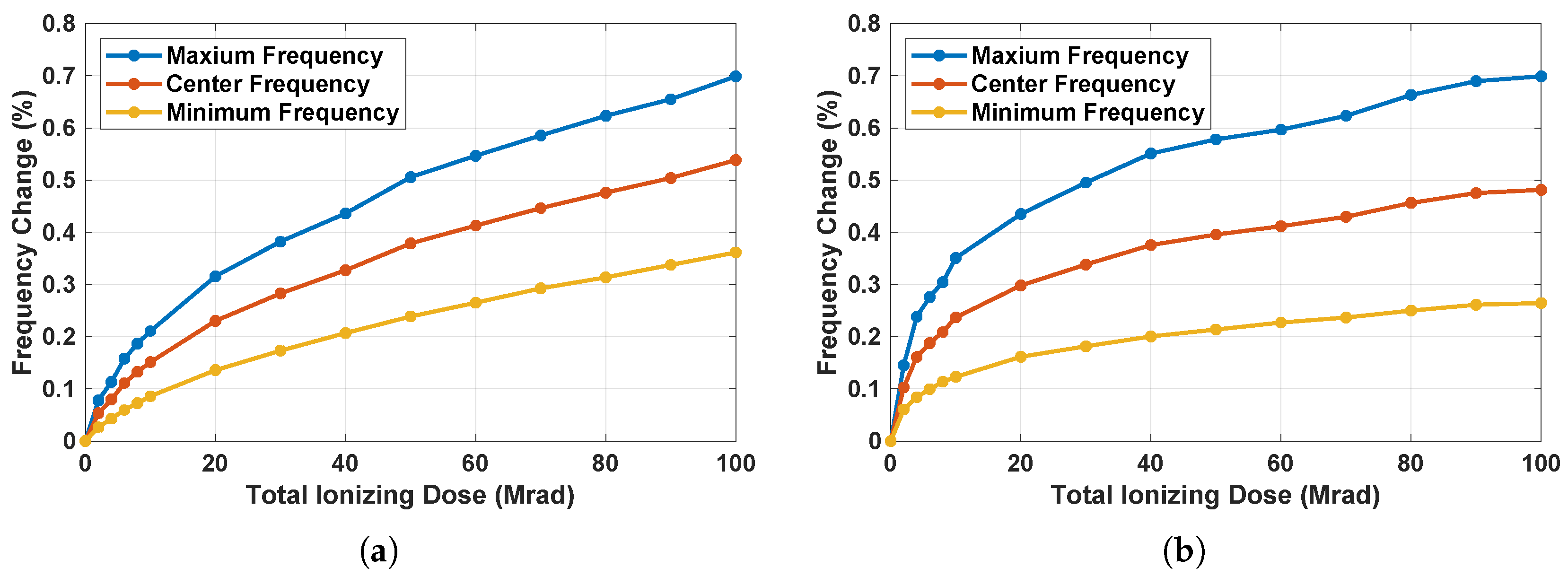
The percentage variations of the measured output frequencies (, and ) of PQVCO and SQVCO are shown in Figure 8a and Figure 8b respectively. Before irradiation, the frequency of the PQVCO ranges from 2.524 GHz to 2.786 GHz with a TR of 9.86% and the frequency of the SQVCO ranges from 2.635 GHz to 2.908 GHz with a TR of 9.88%. Similar to the TID experiments [28,29], the oscillation frequency of both the oscillators gradually increases with respect to TID and an increment of approximately 0.5% can be observed at the center frequency. The increase in the frequency can be accounted for primarily due to the decrease in the transconductances () of the cross-coupled PMOS-NMOS pair with respect to TID [37]. As elaborated in [41], the frequency of oscillation can be expressed as,
where is the tank resonance frequency, is the inductor quality (Q) factor, is the capacitor Q factor, is the capacitance at the common-mode biasing node, is the tank-capacitance, is effective transconductance of the cross-coupled pair, and is the effective impedance at the common-mode biasing mode at the second harmonic of the oscillation frequency.
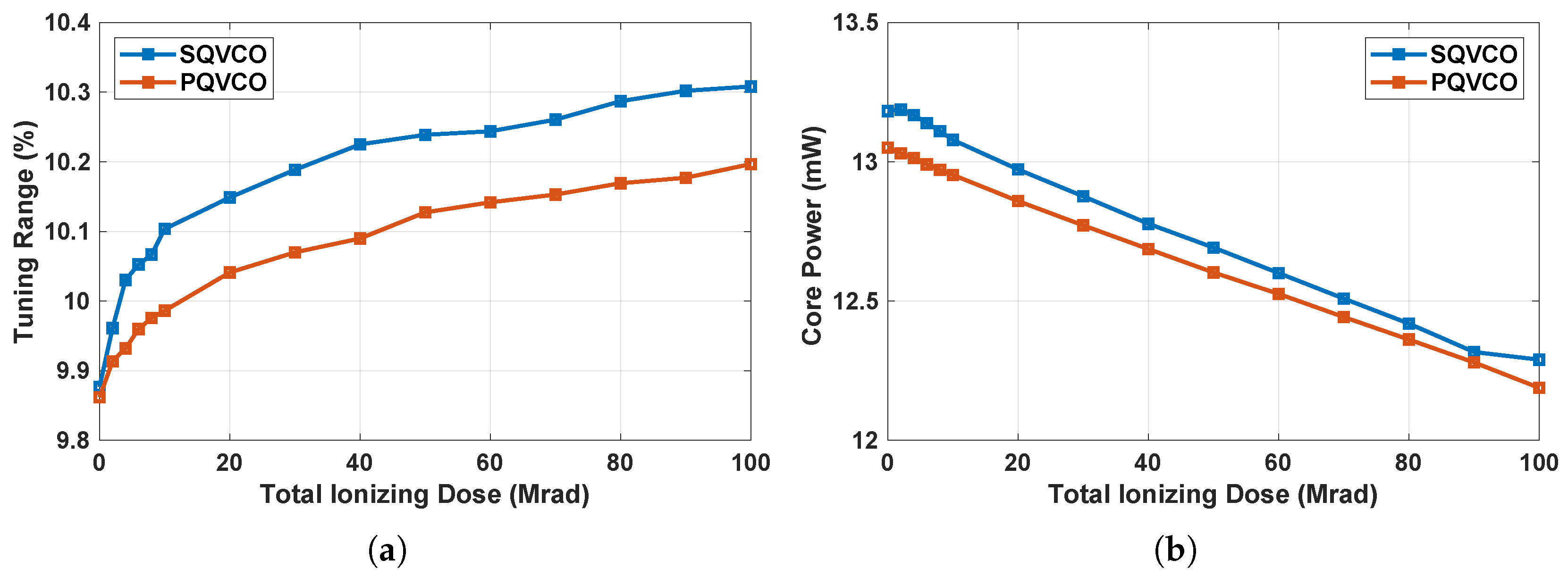
In the oscillators (PQVCO, SQVCO), the NMOS varactors are ac-coupled and therefore are not affected by the level of output common-mode voltages. As the varactor voltage is tuned from 0 to , the varactors’ gate voltage is always greater than the source and drain voltage and so they completely operate in accumulation-mode. The effects of oxide-trap charges and interface trap charges on the varactors with respect to bias voltage are analyzed in detail in [42]. During irradiation, the radiation induced negative charges (oxide-trap and interface trap) result into reduction of the width of the depletion region, which in turn increases the capacitance of the varactors [29,43]. This radiation-induced effect is counteracting previous induced increase in frequency. However, as elaborated in Equation (1) the combined effect of the increase in and the decrease in results in an increase of the frequency of oscillation. In the case of , the contribution of is less compared to that of . For lower values of , the effect of is much more dominant and, therefore, the relative variation of is more than . In the case of SQVCO, the effective impedance at the common-mode biasing node is larger compared to PQVCO because of the resonance of the coupling inductor. Therefore, the increase in the term is less in SQVCO than PQVCO, which results in a slightly larger relative variation of in PQVCO compared to SQVCO. The variations of the TR of the oscillators, which can be expressed as TR = 100 × ( − )/, are measured with respect to TID and shown in Figure 9a. After 100 Mrad (SiO) TID, the relative variation of TR of the PQVCO is 3.4% and that of the SQVCO is 4.4%. In spite of having similar relative variations of for both the oscillators, the relative variation of TR of the PQVCO is less compared to SQVCO primarily due to larger variations of in the PQVCO compared to the SQVCO.
The variations of the dissipated core power of the two different oscillators: SQVCO and PQVCO, are shown in Figure 9b. Before irradiation, the core of the PQVCO consumes a power of 13 mW, whereas the core of the SQVCO consumes a power of 13.2 mW. The dissipated core power reduces with respect to TID and after 100 Mrad (SiO), the core power changes around 7% for both oscillators. NMOS pairs in current-mirror formation with resistive pull-up are used to provide the bias currents to the core of the oscillators. While exposed to radiation, the threshold voltage of the NMOS devices gradually decreases [37], which in turn results in an increased overdrive voltage and a decrease in the current through the resistive pull-up path. Due to mirroring action, the core bias currents also undergo similar reductions. The reduction in bias current also corroborates the fact of increment in oscillation frequency with respect to radiation. As elaborated in [41], the relationship between the oscillation frequency and the bias current is such that when the oscillator is biased at the edge of current-limited region using large bias current, a reduction in bias current shows a slight increase in frequency.
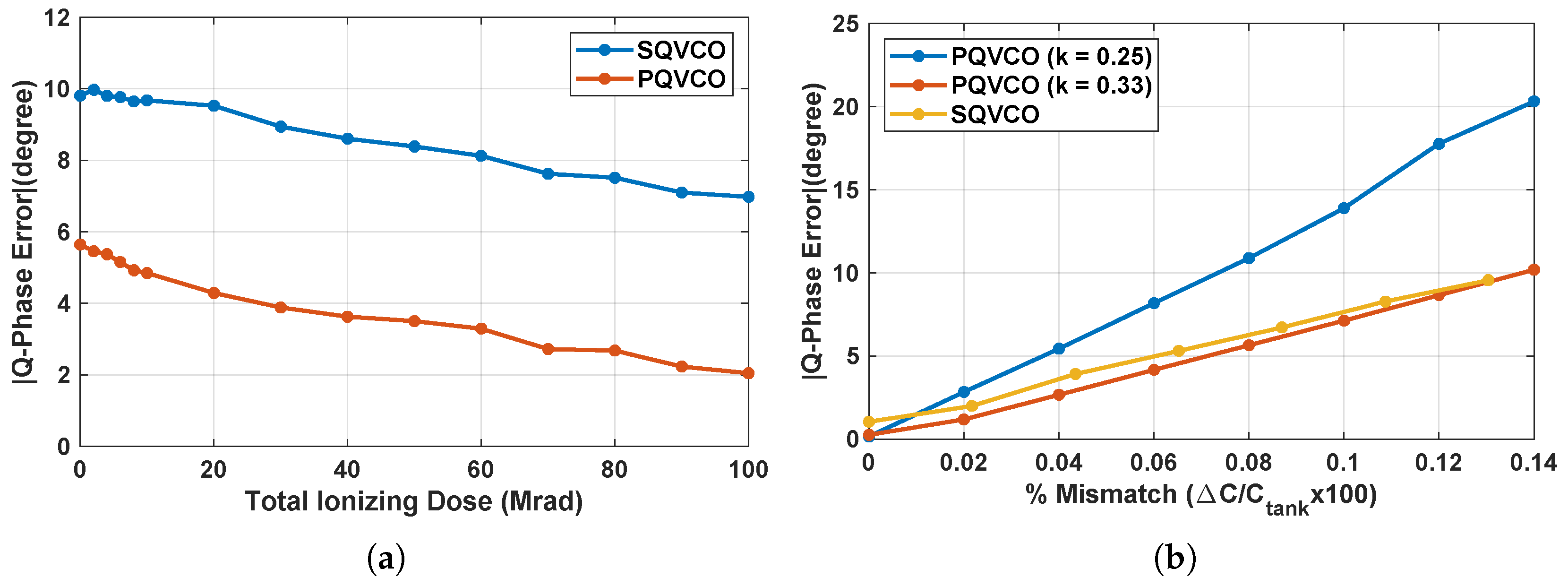
The variations of the absolute Q-phase error of the two oscillators are measured with respect to radiation up to a level of 100 Mrad (SiO). Before irradiation, the Q-phase error is larger (10) in the SQVCO compared to the Q-phase error (5.9) of the PQVCO. The Q-phase error largely depends on the mismatch between the tank resonance of the mutually coupled oscillator cores and the coupling strength of the I/Q phases. The variation of absolute Q-phase error of the two oscillators with respect to the mismatch of based on post-layout simulation results are shown in Figure 10b. With increasing mismatch between of the oscillator cores, the Q-phase error decreases. In the case of the PQVCO, the change in phase error is much more rapid with respect to the mismatch for lower values of the coupling factor (K). During the radiation experiment, the capacitance of the NMOS varactor with respect to the tuning voltage increases with respect to the radiation dose [29,43]. The increasing capacitances eventually reduce the relative mismatch between the . The effect can be seen with respect to radiation as the Q-phase error tends to reduce for both the oscillators as depicted in Figure 10b. As found from the simulation (Figure 10b), increasing the coupling strength (K) diminishes the effects of mismatches.
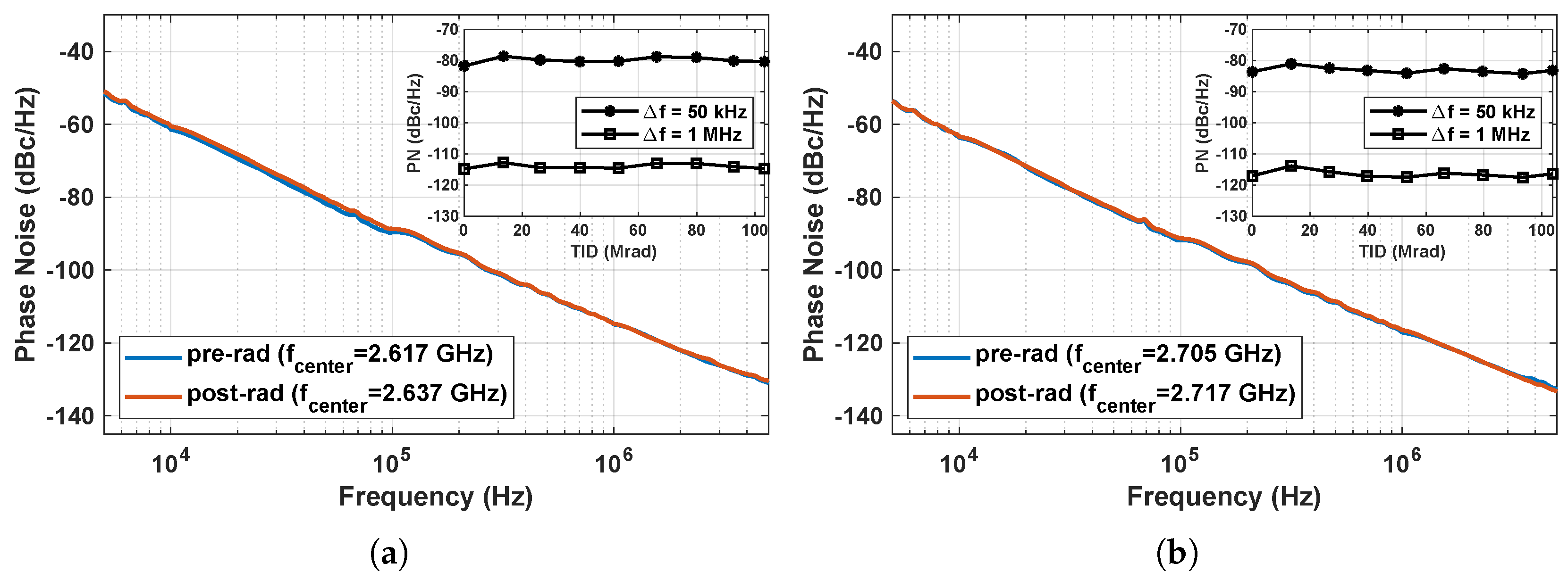
The phase noise characteristics of the PQVCO and the SQVCO measured at frequency are shown in Figure 11a and Figure 11b respectively. The blue lines show the phase noise contributions measured prior to radiation exposure and the red ones show the phase noise observed after 100 Mrad (SiO). As can be observed in Figure 11a,b the phase noise characteristics in the 1/ region (>300 kHz offset) do not undergo much variation. This is counter intuitive with 7% reduction in the bias current. Here, the oscillators are biased at the edge of the current-limited region to produce full swing outputs and achieve optimum phase noise performance. In this region of operation, the changing bias current has minimal effect on the phase noise characteristics [44] of the oscillators. Although, the thermal noise contribution of the cross-coupled core devices are supposed to increase with respect to TID [45], the overall phase noise characteristics in the 1/ region does not change much. This is primarily due to the wider device sizes as used in the cross-coupled pairs which reduce the thermal noise contributions in the phase noise characteristics. However, a close observation can reveal the close-in phase noise in the 1/ region (<300 kHz offset) increases slightly in the case of the PQVCO compared to the SQVCO. This is due to the extra pair of NMOS devices used for coupling the I and Q phases. The sizes of the devices are less compared to the core devices (coupling factor K = 0.25), and therefore contribute more 1/f noise. Overall, the phase noise characteristic of the SQVCO is slightly better than for the PQVCO due to the tail-noise filter [40] in the form of the coupling inductor present in the SQVCO.
Table 1 presents a performance comparison of the implemented QVCOs with respect to previously reported VCOs [28,29,46,47] and QVCOs [33] which are studied under radiation (TID) exposure. Similar to [28], the implemented QVCOs in this work are targeted to operate in the s-band. The implemented QVCOs consume double power in comparison with [28] as two oscillator cores are coupled together to generate quadrature phases. Based on open loop phase noise characteristics, the implemented QVCOs achieve more than 3 dB better phase noise at 1 MHz offset. However, [28] has a similar rate of variations of the frequency with respect to TID level when compared to the implemented QVCOs. The oscillator in [47] has combined small varactors with large digitally switchable capacitor-banks (64 units) and therefore could achieve better phase noise performance compared to the other reported designs. Prior to this work as published in the literature to date, ref. [33] has been the sole instance of TID study performed on QVCOs. Therefore, the results are included in the comparison, even though it is implemented using a 32 nm CMOS SOI technology which is different from the one used in this work. Although TID induced variations tend to reduce with smaller feature sizes, the QVCOs reported in [33] show more frequency variation and less TID tolerance compared to the QVCOs implemented in this work.
4. Conclusions
The performance study and evaluation of radiation induced effects on the prototypes of the QVCOs: PQVCO and SQVCO are presented in this article. It shall help to understand the vulnerabilities of the implementation and thereby improve the design for future implementations. The samples of the prototypes are tested under X-ray radiation up to a level of 100 Mrad (SiO). Prior to radiation exposure, the measured frequency of the PQVCO ranges from 2.524 GHz to 2.786 GHz with a TR of 9.86% and the measured frequency of the SQVCO ranges from 2.635 GHz to 2.908 GHz with a TR of 9.88%. The overall variations of the frequencies of the oscillators are less than 1% and change in TR is less than 5% after the radiation exposure, which makes them suitable to be integrated inside phase-locked-loops (PLLs) and half-rate CDRs. Although the bias current reduces by 7% after 100 Mrad (SiO) irradiation, it has little contribution on the phase noise performance of the QVCOs. The most vulnerable performance metric is the Q-phase error of the oscillators. Here, in this experiment the decreasing relative mismatch between the improves the Q-phase error. In the case of the oscillator SQVCO the Q-phase error improves from 10 to 7 and in the case of the oscillators PQVCO, it improves from 5.9 to 2. However, for applications involving much higher frequencies, the value of used would be less, which may worsen the radiation induced variations in Q-phase. The solution would be to increase the coupling strength in the PQVCO to minimize the mismatch induced variations at the expense of phase noise performance. In the case of SQVCO, extra effort is needed to produce matching layouts of the oscillator cores for reducing the mismatch.
Author Contributions
Conceptualization, A.K., V.D.S. and P.L.; Data curation, A.K.; Investigation, A.K.; Methodology, A.K., V.D.S. and P.L.; Supervision, V.D.S. and P.L.; Writing—original draft, A.K.; Writing—review and editing, A.K., V.D.S. and P.L. All authors have read and agreed to the published version of the manuscript.
Funding
This work is funded by the European’s Union Horizon 2020 Research and Innovation Programme under grant agreement number 721624 ‘RADSAGA’.
Institutional Review Board Statement
Not applicable.
Informed Consent Statement
Not applicable.
Data Availability Statement
Not applicable.
Conflicts of Interest
The authors declare no conflict of interest. The funders had no role in the design of the study; in the collection, analyses, or interpretation of data; in the writing of the manuscript, or in the decision to publish the results.
References
- Musa, A.; Murakami, R.; Sato, T.; Chaivipas, W.; Okada, K.; Matsuzawa, A. A Low Phase Noise Quadrature Injection Locked Frequency Synthesizer for MM-Wave Applications. IEEE J. Solid-State Circuits 2011, 46, 2635–2649. [Google Scholar] [CrossRef]
- Chamas, I.R.; Raman, S. Analysis and Design of a CMOS Phase-Tunable Injection-Coupled LC Quadrature VCO (PTIC-QVCO). IEEE J. Solid-State Circuits 2009, 44, 784–796. [Google Scholar] [CrossRef]
- Eroglu, A. Non-Invasive Quadrature Modulator Balancing Method to Optimize Image Band Rejection. IEEE Trans. Circuits Syst. I Regul. Pap. 2014, 61, 600–612. [Google Scholar] [CrossRef]
- Nikoofard, A.; Kananian, S.; Fotowat-Ahmady, A. A fully analog calibration technique for phase and gain mismatches in image-reject receivers. AEU-Int. J. Electron. Commun. 2015, 69, 823–835. [Google Scholar] [CrossRef]
- Lee, J.; Razavi, B. A 40-Gb/s clock and data recovery circuit in 0.18-μm CMOS technology. IEEE J. Solid-State Circuits 2003, 38, 2181–2190. [Google Scholar] [CrossRef]
- Mazzanti, A.; Svelto, F.; Andreani, P. On the amplitude and phase errors of quadrature LC-tank CMOS oscillators. IEEE J. Solid-State Circuits 2006, 41, 1305–1313. [Google Scholar] [CrossRef]
- Natarajan, A.; Komijani, A.; Guan, X.; Babakhani, A.; Hajimiri, A. A 77-GHz Phased-Array Transceiver with On-Chip Antennas in Silicon: Transmitter and Local LO-Path Phase Shifting. IEEE J. Solid-State Circuits 2006, 41, 2807–2819. [Google Scholar] [CrossRef] [Green Version]
- Scheir, K.; Bronckers, S.; Borremans, J.; Wambacq, P.; Rolain, Y. A 52 GHz Phased-Array Receiver Front-End in 90 nm Digital CMOS. IEEE J. Solid-State Circuits 2008, 43, 2651–2659. [Google Scholar] [CrossRef]
- Nikoofard, A.; Kananian, S.; Fotowat-Ahmady, A. Off-Resonance Oscillation, Phase Retention, and Orthogonality Modeling in Quadrature Oscillators. IEEE Trans. Circuits Syst. I Regul. Pap. 2016, 63, 883–894. [Google Scholar] [CrossRef]
- Zhang, L.; Kuo, N.C.; Niknejad, A.M. A 37.5–45 GHz Superharmonic-Coupled QVCO with Tunable Phase Accuracy in 28 nm CMOS. IEEE J. Solid-State Circuits 2019, 54, 2754–2764. [Google Scholar] [CrossRef]
- Oliveira, L.B.; Fernandes, J.R.; Filanovsky, I.M.; Verhoeven, C.J.; Silva, M.M. Analysis and Design of Quadrature Oscillators; Springer Science & Business Media: Berlin/Heidelberg, Germany, 2008. [Google Scholar]
- Koo, J.; Kim, B.; Park, H.J.; Sim, J.Y. A Quadrature RC Oscillator with Noise Reduction by Voltage Swing Control. IEEE Trans. Circuits Syst. I Regul. Pap. 2019, 66, 3077–3088. [Google Scholar] [CrossRef]
- Dai, L.; Harjani, R. A low-phase-noise CMOS ring oscillator with differential control and quadrature outputs. In Proceedings of the 14th Annual IEEE International ASIC/SOC Conference (IEEE Cat. No.01TH8558), Arlington, VA, USA, 12–15 September 2001; pp. 134–138. [Google Scholar] [CrossRef]
- Pankratz, E.J.; Sanchez-Sinencio, E. Multiloop High-Power-Supply-Rejection Quadrature Ring Oscillator. IEEE J. Solid-State Circuits 2012, 47, 2033–2048. [Google Scholar] [CrossRef]
- Behbahani, F.; Kishigami, Y.; Leete, J.; Abidi, A. CMOS mixers and polyphase filters for large image rejection. IEEE J. Solid-State Circuits 2001, 36, 873–887. [Google Scholar] [CrossRef] [Green Version]
- Sah, S.P.; Yu, X.; Heo, D. Design and Analysis of a Wideband 15–35-GHz Quadrature Phase Shifter with Inductive Loading. IEEE Trans. Microw. Theory Tech. 2013, 61, 3024–3033. [Google Scholar] [CrossRef]
- Lee, T.H. The Design of CMOS Radio-Frequency Integrated Circuits; Cambridge University Press: Cambridge, UK, 2003. [Google Scholar]
- Andreani, P.; Bonfanti, A.; Romano, L.; Samori, C. Analysis and design of a 1.8-GHz CMOS LC quadrature VCO. IEEE J. Solid-State Circuits 2002, 37, 1737–1747. [Google Scholar] [CrossRef]
- Chang, H.Y.; Chiu, Y.T. K-Band CMOS Differential and Quadrature Voltage-Controlled Oscillators for Low Phase-Noise and Low-Power Applications. IEEE Trans. Microw. Theory Tech. 2012, 60, 46–59. [Google Scholar] [CrossRef]
- Chang, H.Y.; Lin, C.H.; Liu, Y.C.; Yeh, Y.L.; Chen, K.; Wu, S.H. 65-nm CMOS Dual-Gate Device for Ka-Band Broadband Low-Noise Amplifier and High-Accuracy Quadrature Voltage-Controlled Oscillator. IEEE Trans. Microw. Theory Tech. 2013, 61, 2402–2413. [Google Scholar] [CrossRef]
- Decanis, U.; Ghilioni, A.; Monaco, E.; Mazzanti, A.; Svelto, F. A Low-Noise Quadrature VCO Based on Magnetically Coupled Resonators and a Wideband Frequency Divider at Millimeter Waves. IEEE J. Solid-State Circuits 2011, 46, 2943–2955. [Google Scholar] [CrossRef]
- Kuo, N.C.; Chien, J.C.; Niknejad, A.M. Design and Analysis on Bidirectionally and Passively Coupled QVCO with Nonlinear Coupler. IEEE Trans. Microw. Theory Tech. 2015, 63, 1130–1141. [Google Scholar] [CrossRef]
- Karmakar, A.; Wang, J.; Prinzie, J.; De Smedt, V.; Leroux, P. A Review of Semiconductor Based Ionising Radiation Sensors Used in Harsh Radiation Environments and Their Applications. Radiation 2021, 1, 194–217. [Google Scholar] [CrossRef]
- Faccio, F.; Michelis, S.; Cornale, D.; Paccagnella, A.; Gerardin, S. Radiation-Induced Short Channel (RISCE) and Narrow Channel (RINCE) Effects in 65 and 130 nm MOSFETs. IEEE Trans. Nucl. Sci. 2015, 62, 2933–2940. [Google Scholar] [CrossRef]
- Borghello, G. Ionizing Radiation Effects in Nanoscale CMOS Technologies Exposed to Ultra-High Doses. Ph.D. Thesis, University of Udine, Udine, Italy, 2019. [Google Scholar]
- Borghello, G.; Lerario, E.; Faccio, F.; Koch, H.; Termo, G.; Michelis, S.; Marquez, F.; Palomo, F.; Muñoz, F. Ionizing radiation damage in 65 nm CMOS technology: Influence of geometry, bias and temperature at ultra-high doses. Microelectron. Reliab. 2021, 116, 114016. [Google Scholar] [CrossRef]
- Wang, T.; Wang, K.; Chen, L.; Dinh, A.; Bhuva, B.; Shuler, R. A RHBD LC-Tank Oscillator Design Tolerant to Single-Event Transients. IEEE Trans. Nucl. Sci. 2010, 57, 3620–3625. [Google Scholar] [CrossRef]
- Prinzie, J.; Christiansen, J.; Moreira, P.; Steyaert, M.; Leroux, P. Comparison of a 65 nm CMOS Ring- and LC-Oscillator Based PLL in Terms of TID and SEU Sensitivity. IEEE Trans. Nucl. Sci. 2017, 64, 245–252. [Google Scholar] [CrossRef]
- Monda, D.; Ciarpi, G.; Saponara, S. Design and Verification of a 6.25 GHz LC-Tank VCO Integrated in 65 nm CMOS Technology Operating up to 1 Grad TID. IEEE Trans. Nucl. Sci. 2021, 68, 2524–2532. [Google Scholar] [CrossRef]
- Jagtap, S.; Sharma, D.; Gupta, S. Design of SET tolerant LC oscillators using distributed bias circuitry. Microelectron. Reliab. 2015, 55, 1537–1541. [Google Scholar] [CrossRef]
- Karthigeyan, A.; Radha, S.; Manikandan, E. Single event transient mitigation techniques for a cross-coupled LC oscillator, including a single-event transient hardened CMOS LC-VCO circuit. IET Circuits Devices Syst. 2022, 16, 178–188. [Google Scholar] [CrossRef]
- Jagtap, S.; Anmadwar, S.; Rudrapati, S.; Gupta, S. A Single-Event Transient-Tolerant High-Frequency CMOS Quadrature Phase Oscillator. IEEE Trans. Nucl. Sci. 2019, 66, 2072–2079. [Google Scholar] [CrossRef]
- Loveless, T.D.; Jagannathan, S.; Zhang, E.X.; Fleetwood, D.M.; Kauppila, J.S.; Haeffner, T.D.; Massengill, L.W. Combined Effects of Total Ionizing Dose and Temperature on a K-Band Quadrature LC-Tank VCO in a 32 nm CMOS SOI Technology. IEEE Trans. Nucl. Sci. 2017, 64, 204–211. [Google Scholar] [CrossRef]
- Chamas, I.R.; Raman, S. A Comprehensive Analysis of Quadrature Signal Synthesis in Cross-Coupled RF VCOs. IEEE Trans. Circuits Syst. I Regul. Pap. 2007, 54, 689–704. [Google Scholar] [CrossRef]
- Mirzaei, A.; Heidari, M.E.; Bagheri, R.; Chehrazi, S.; Abidi, A.A. The Quadrature LC Oscillator: A Complete Portrait Based on Injection Locking. IEEE J. Solid-State Circuits 2007, 42, 1916–1932. [Google Scholar] [CrossRef]
- Prinzie, J.; Christiansen, J.; Moreira, P.; Steyaert, M.; Leroux, P. A 2.56-GHz SEU Radiation Hard LC-Tank VCO for High-Speed Communication Links in 65-nm CMOS Technology. IEEE Trans. Nucl. Sci. 2018, 65, 407–412. [Google Scholar] [CrossRef]
- Menouni, M.; Barbero, M.; Bompard, F.; Bonacini, S.; Fougeron, D.; Gaglione, R.; Rozanov, A.; Valerio, P.; Wang, A. 1-Grad total dose evaluation of 65 nm CMOS technology for the HL-LHC upgrades. J. Instrum. 2015, 10, C05009. [Google Scholar] [CrossRef] [Green Version]
- Tong, H.; Cheng, S.; Lo, Y.C.; Karsilayan, A.I.; Silva-Martinez, J. An LC Quadrature VCO Using Capacitive Source Degeneration Coupling to Eliminate Bi-Modal Oscillation. IEEE Trans. Circuits Syst. I Regul. Pap. 2012, 59, 1871–1879. [Google Scholar] [CrossRef]
- Gierkink, S.; Levantino, S.; Frye, R.; Samori, C.; Boccuzzi, V. A low-phase-noise 5-GHz CMOS quadrature VCO using superharmonic coupling. IEEE J. Solid-State Circuits 2003, 38, 1148–1154. [Google Scholar] [CrossRef]
- Hegazi, E.; Sjoland, H.; Abidi, A. A filtering technique to lower LC oscillator phase noise. IEEE J. Solid-State Circuits 2001, 36, 1921–1930. [Google Scholar] [CrossRef] [Green Version]
- Wu, T.; Moon, U.K.; Mayaram, K. Dependence of LC VCO oscillation frequency on bias current. In Proceedings of the 2006 IEEE International Symposium on Circuits and Systems (ISCAS), Island of Kos, Greece, 21–24 May 2006; p. 4. [Google Scholar] [CrossRef] [Green Version]
- Heiman, F.; Warfield, G. The effects of oxide traps on the MOS capacitance. IEEE Trans. Electron Devices 1965, 12, 167–178. [Google Scholar] [CrossRef] [Green Version]
- Fernández-Martínez, P.; Cortés, I.; Hidalgo, S.; Flores, D.; Palomo, F.R. Simulation of Total Ionising Dose in MOS capacitors. In Proceedings of the 8th Spanish Conference on Electron Devices, CDE’2011, Palma de Mallorca, Spain, 8–11 February 2011; pp. 1–4. [Google Scholar] [CrossRef]
- Rael, J.; Abidi, A.A. Physical processes of phase noise in differential LC oscillators. In Proceedings of the IEEE 2000 Custom Integrated Circuits Conference (Cat. No. 00CH37044), Orlando, FL, USA, 24 May 2000; pp. 569–572. [Google Scholar]
- Re, V.; Gaioni, L.; Manghisoni, M.; Ratti, L.; Traversi, G. Comprehensive Study of Total Ionizing Dose Damage Mechanisms and Their Effects on Noise Sources in a 90 nm CMOS Technology. IEEE Trans. Nucl. Sci. 2008, 55, 3272–3279. [Google Scholar] [CrossRef]
- Mazza, G.; Panati, S. A Compact, Low Jitter, CMOS 65 nm 4.8–6 GHz Phase-Locked Loop for Applications in HEP Experiments Front-End Electronics. IEEE Trans. Nucl. Sci. 2018, 65, 1212–1217. [Google Scholar] [CrossRef]
- Biereigel, S.; Kulis, S.; Leitao, P.; Francisco, R.; Moreira, P.; Leroux, P.; Prinzie, J. A low noise fault tolerant radiation hardened 2.56 Gbps clock-data recovery circuit with high speed feed forward correction in 65 nm CMOS. IEEE Trans. Circuits Syst. I Regul. Pap. 2019, 67, 1438–1446. [Google Scholar] [CrossRef]
Figure 1.
A schematic representation of the parallel coupled quadrature LC-tank VCO (PQVCO).

Figure 2.
(a) Tunable LC-tank circuit with ac-coupled NMOS varactor, (b) ring oscillators for phase lead/lag selection, and (c) oscillator generated output waveforms for different ring oscillator configurations.
Figure 2.
(a) Tunable LC-tank circuit with ac-coupled NMOS varactor, (b) ring oscillators for phase lead/lag selection, and (c) oscillator generated output waveforms for different ring oscillator configurations.

Figure 3.
A simplified block diagram of the PQVCO where two oscillator cores are coupled with each other through transconductance () circuit.
Figure 3.
A simplified block diagram of the PQVCO where two oscillator cores are coupled with each other through transconductance () circuit.
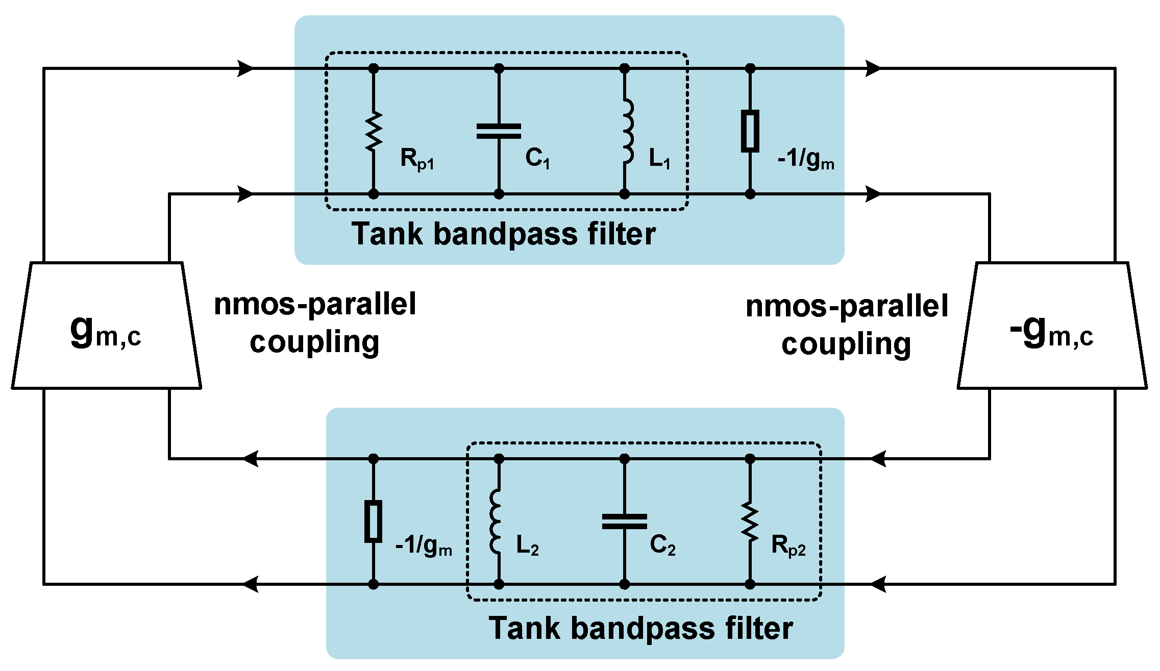
Figure 4.
A schematic representation of the super-harmonic coupled quadrature LC-tank VCO (SQVCO).
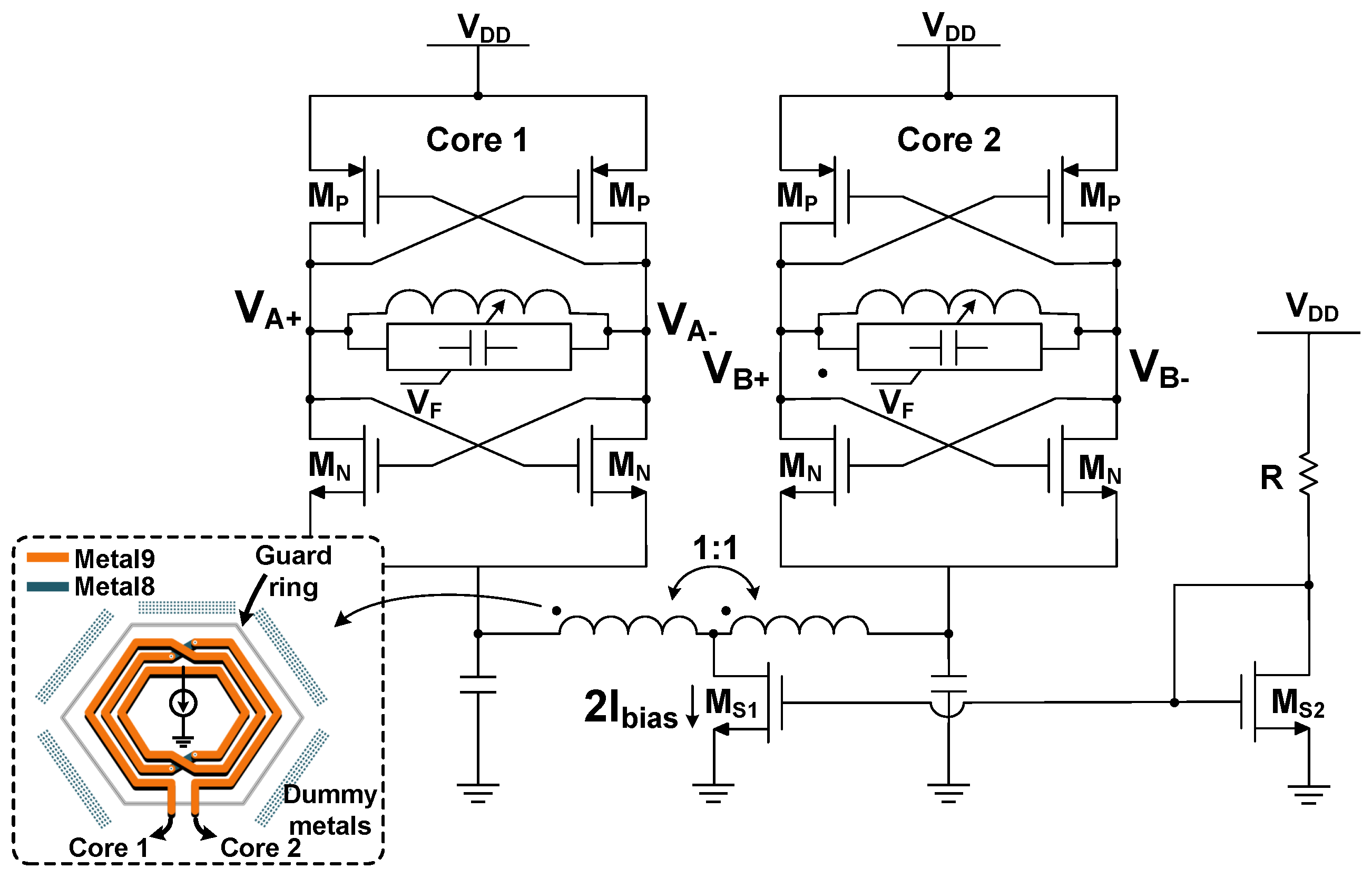
Figure 5.
A simplified block diagram of the SQVCO where two oscillator cores coupled with each other through a center-tap inductor.
Figure 5.
A simplified block diagram of the SQVCO where two oscillator cores coupled with each other through a center-tap inductor.
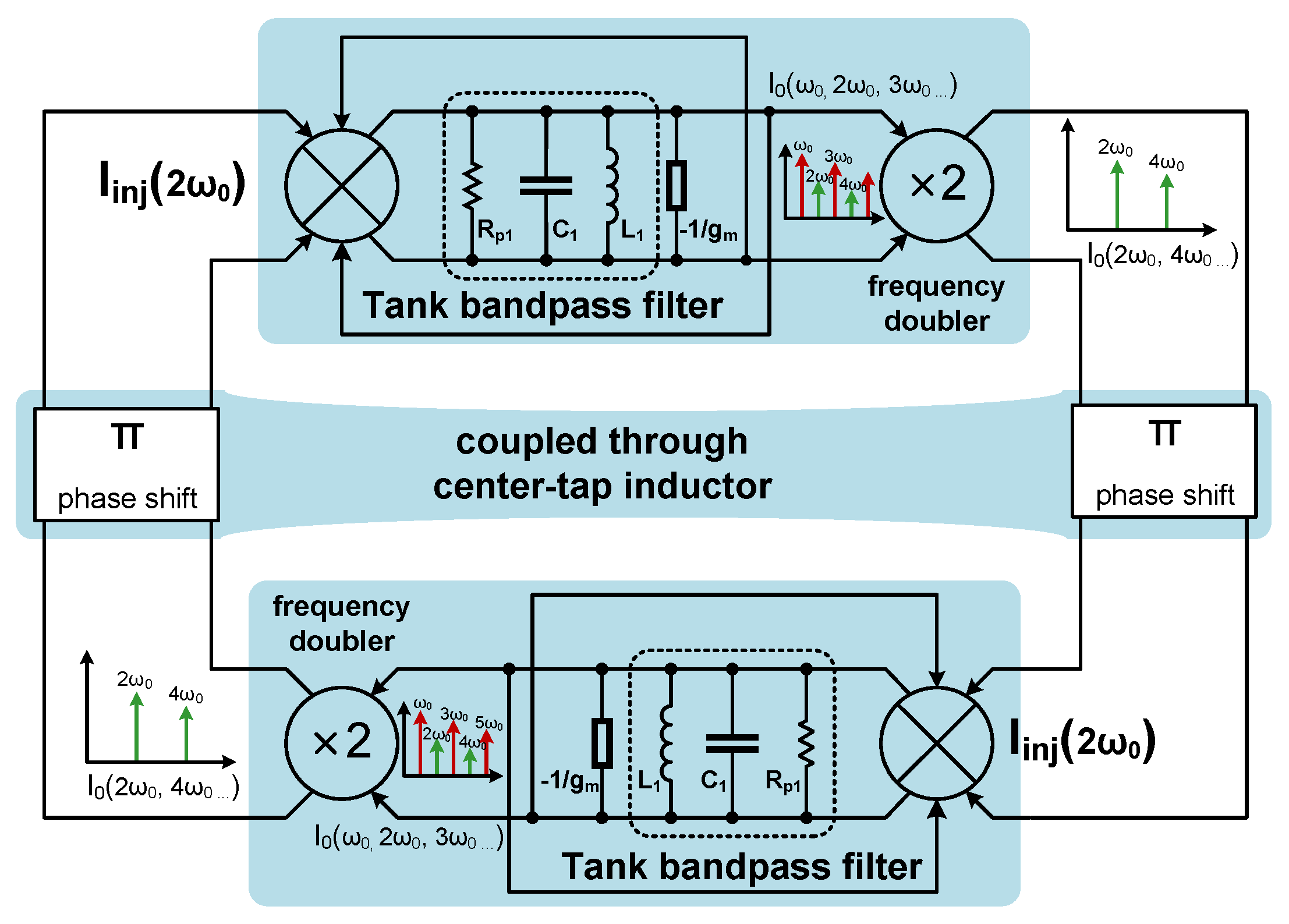
Figure 6.
Cascaded CMOS digital buffers used at the oscillator outputs.
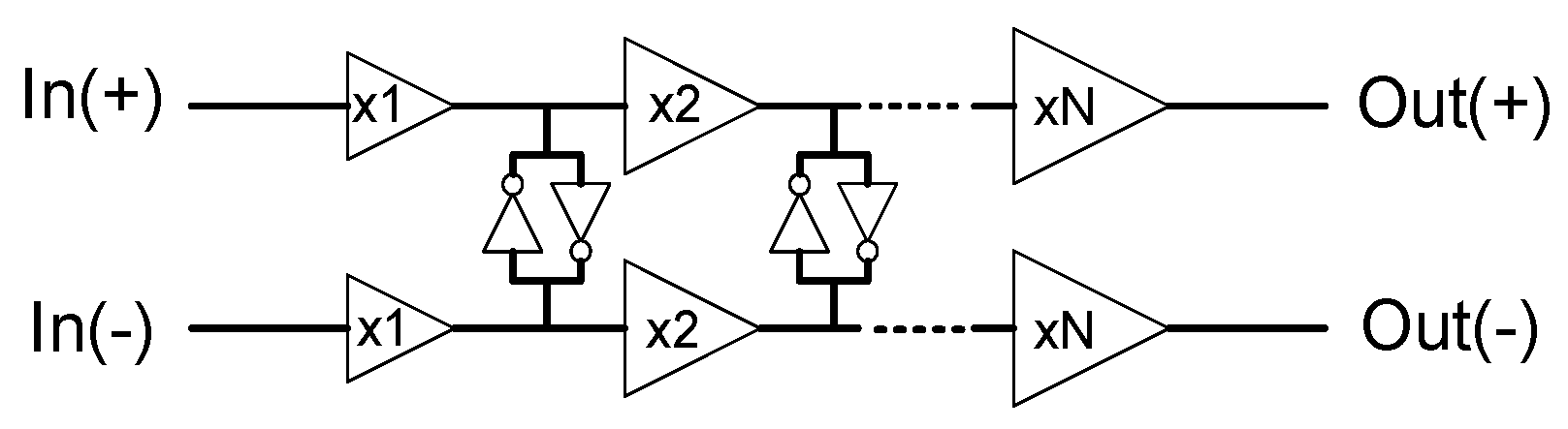
Figure 7.
Overview of test setup for radiation assessment of QVCOs and the micrograph of the die (2 mm × 2 mm) in the top right corner.
Figure 7.
Overview of test setup for radiation assessment of QVCOs and the micrograph of the die (2 mm × 2 mm) in the top right corner.

Figure 8.
Percentage frequency variations of (a) PQVCO and (b) SQVCO measured with respect to the TID of the order of 100 Mrad (SiO).
Figure 8.
Percentage frequency variations of (a) PQVCO and (b) SQVCO measured with respect to the TID of the order of 100 Mrad (SiO).

Figure 9.
(a) Tuning ranges, (b) core power consumption of SQVCO and PQVCO measured with respect to the TID of the order of 100 Mrad (SiO).
Figure 9.
(a) Tuning ranges, (b) core power consumption of SQVCO and PQVCO measured with respect to the TID of the order of 100 Mrad (SiO).

Figure 10.
(a) Variations of Q-phase error measured with respect to TID of 100 Mrad (SiO), (b) simulated Q-phase error for the SQVCO and PQVCO with respect to different relative mismatch in .
Figure 10.
(a) Variations of Q-phase error measured with respect to TID of 100 Mrad (SiO), (b) simulated Q-phase error for the SQVCO and PQVCO with respect to different relative mismatch in .

Figure 11.
Phase noise measured at before (pre-rad) and after (post-rad) radiation exposure of the order of 100 Mrad (SiO) from the outputs of the (a) PQVCO and (b) SQVCO.
Figure 11.
Phase noise measured at before (pre-rad) and after (post-rad) radiation exposure of the order of 100 Mrad (SiO) from the outputs of the (a) PQVCO and (b) SQVCO.


Table 1.
Performance comparison with respect to previously published VCOs and QVCOs which are tested under radiation (TID).
Table 1.
Performance comparison with respect to previously published VCOs and QVCOs which are tested under radiation (TID).
| Reference | TNS’17 [28] | TNS’18 [36] | TNS’18 [46] | TCASI’19 [47] | TNS’21 [29] | TNS’17 [33] | This Work | |
|---|---|---|---|---|---|---|---|---|
| Technology (nm) | 65 | 65 | 65 | 65 | 65 | 32 | 65 | |
| Type | VCO | VCO | VCO | VCO | VCO | QVCO | QVCO | QVCO |
| Oscillator Area (mm) | - | - | 0.124 | - | 0.061 | 0.0484 | 0.458 | 0.367 |
| Frequency (GHz) | 2.2–3.2 | 2.5–2.65 | 4.8–6.0 | 4.9–5.2 | 5.4–6.8 | 20.1–20.7 | 2.6–2.9 | 2.5–2.8 |
| Tuning Range (%) | 30 ** | 5.8 | 4 | 5.9 ** | 23 | 3 | 9.9 | |
| Phase Noise @1 MHz (dBc/Hz) | −110 | −118 | - | −122 | −100 | −99 | −119 | −115 |
| VCO Gain (MHz/V) | 240 ** | - | 1850 | 100 ** | 225 | 610 | 273 | 262 |
| Power (mW) | 6 | 1.8 | 18 | 34 | 2.85 | 12.8 | 13.2 | 13 |
| FoM (dBc/Hz) | −171 | −188.7 | - | −180 | −171.4 | −176 | −176.4 | −172.2 |
| Frequency Change (%) | 3.5 | - | - | 3.2 | 2.54 | 1.4 | 0.7 | |
| TID Tolerance | 600 | - | 250 | 350 | 1000 | 0.5 | 100 | |
§ FoM = Phase Noise@Δf − 20log() + 10log(). † SQVCO, ‡ PQVCO. §§ Open-loop phase noise, ** Varactors and digitally-controlled capacitor-banks used.
Publisher’s Note: MDPI stays neutral with regard to jurisdictional claims in published maps and institutional affiliations. |
© 2022 by the authors. Licensee MDPI, Basel, Switzerland. This article is an open access article distributed under the terms and conditions of the Creative Commons Attribution (CC BY) license (https://creativecommons.org/licenses/by/4.0/).
Share and Cite
MDPI and ACS Style
Karmakar, A.; De Smedt, V.; Leroux, P. TID Sensitivity Assessment of Quadrature LC-Tank VCOs Implemented in 65-nm CMOS Technology. Electronics 2022, 11, 1399. https://doi.org/10.3390/electronics11091399
AMA Style
Karmakar A, De Smedt V, Leroux P. TID Sensitivity Assessment of Quadrature LC-Tank VCOs Implemented in 65-nm CMOS Technology. Electronics. 2022; 11(9):1399. https://doi.org/10.3390/electronics11091399
Chicago/Turabian StyleKarmakar, Arijit, Valentijn De Smedt, and Paul Leroux. 2022. "TID Sensitivity Assessment of Quadrature LC-Tank VCOs Implemented in 65-nm CMOS Technology" Electronics 11, no. 9: 1399. https://doi.org/10.3390/electronics11091399
Note that from the first issue of 2016, this journal uses article numbers instead of page numbers. See further details here.