
CMOS Front End for Interfacing Spin-Hall Nano-Oscillators for Neuromorphic Computing in the GHz Range

 ,
, 
Abstract
:1. Introduction
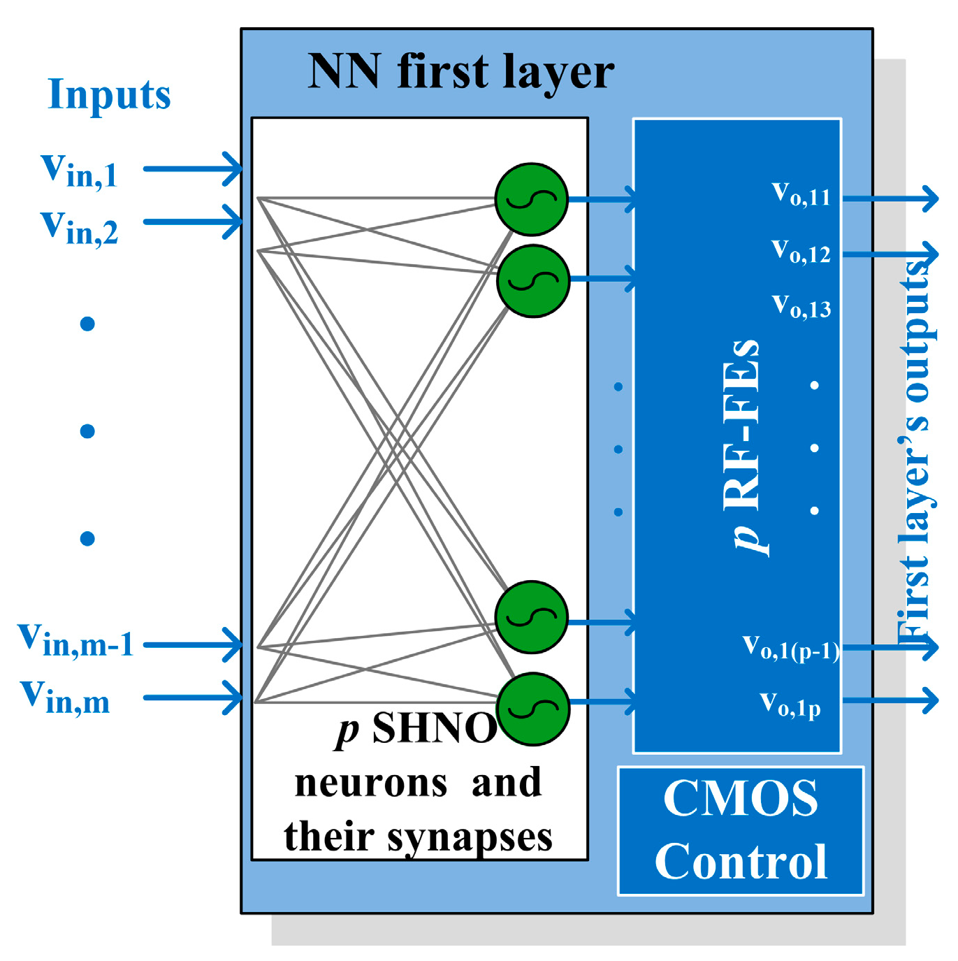
2. NCS Scheme
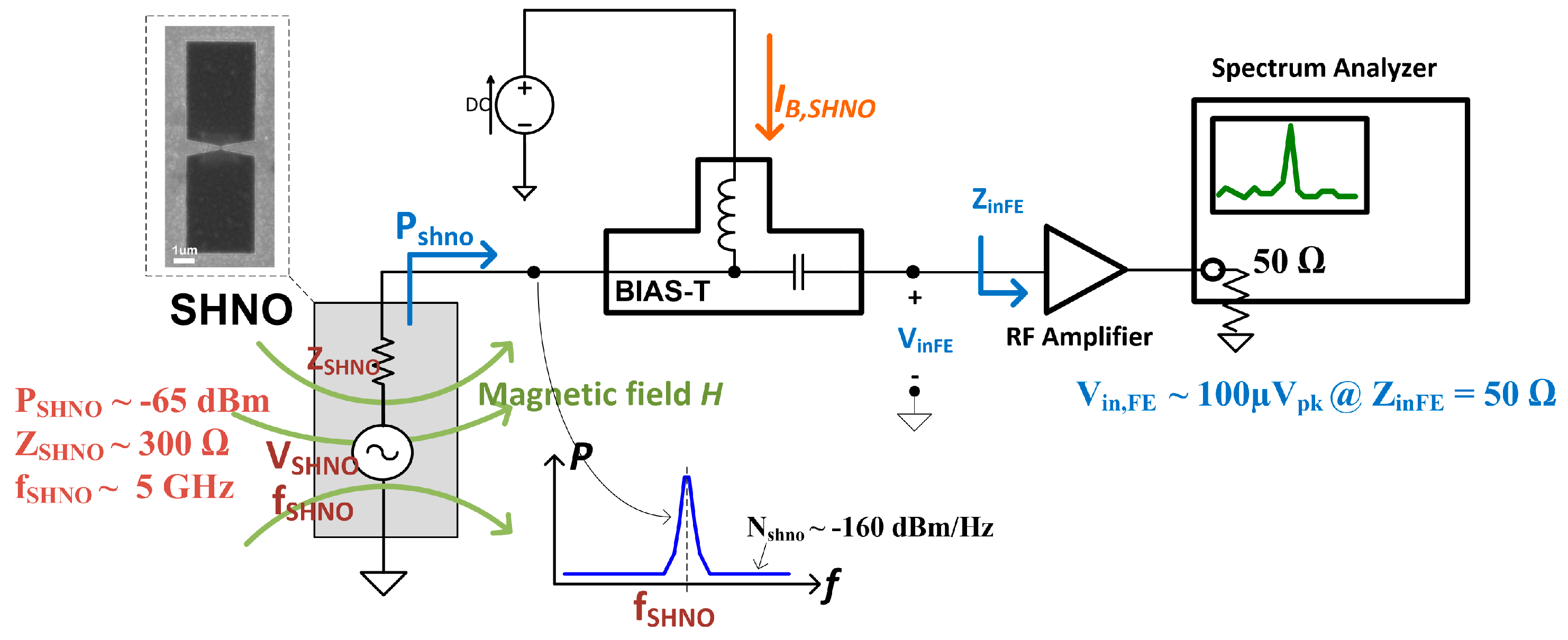
3. SHNO Electrical Model
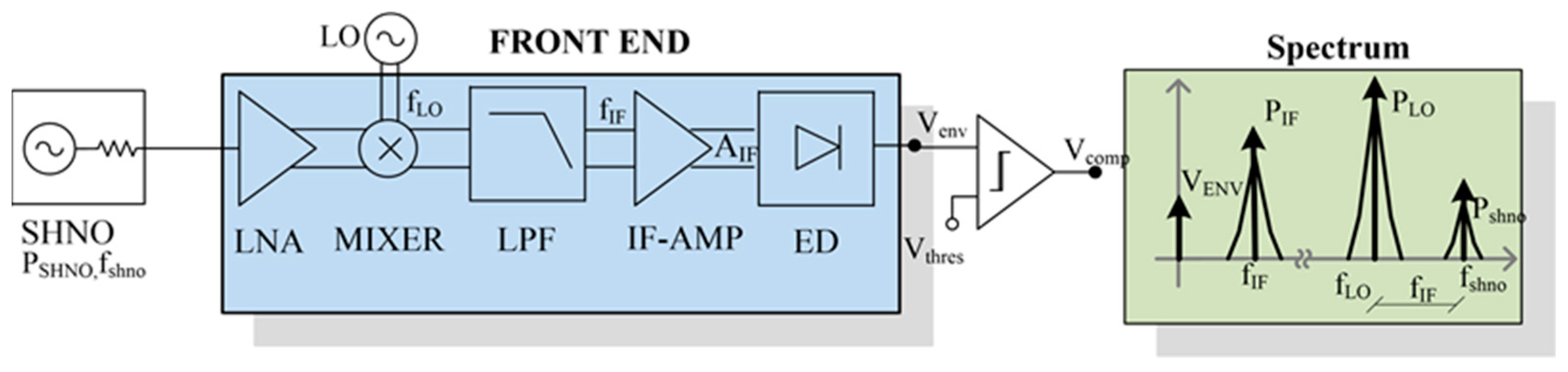
4. RF Front End
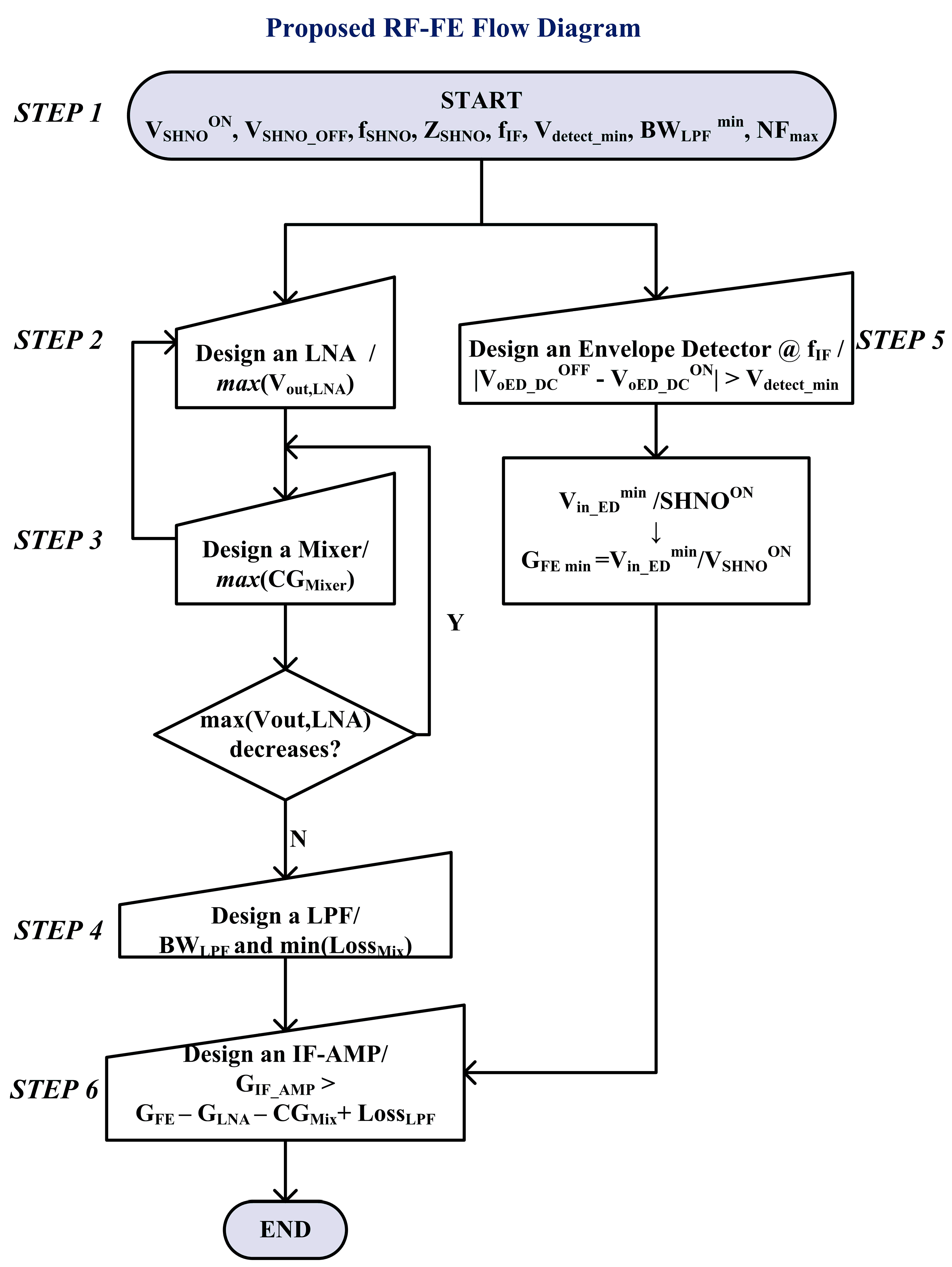
- STEP 1.
- Start by fixing a set of initial parameters and limits: SHNO voltage where it is considered to be turned on and off, VSHNOON/OFF, SHNO oscillation frequency fSHNO, SHNO output impedance ZSHNO, intermediate-frequency fIF, voltage difference that the comparator can discern, Vdetect_min, minimum bandwidth of the LPF, BWLPFmin, and maximum noise figure NFmax of the RF-FE.
- STEP 2.
- Design an LNA that maximizes its output voltage, Vout,LNA at fSHNO, and whose noise figure NF is below NFmax. (Maximizing Vout,LNA implicitly means improve a good LNA input matching).
- STEP 3.
- Design a mixer (co-designed with the LNA) that maximizes its conversion gain CGMixer. If Vout,LNA is substantially reduced (i.e., if the mixer excessively loads the LNA), a new mixer should be designed. If it is not possible, a new LNA architecture should be chosen to cope with the load fixed by the mixer.
- STEP 4.
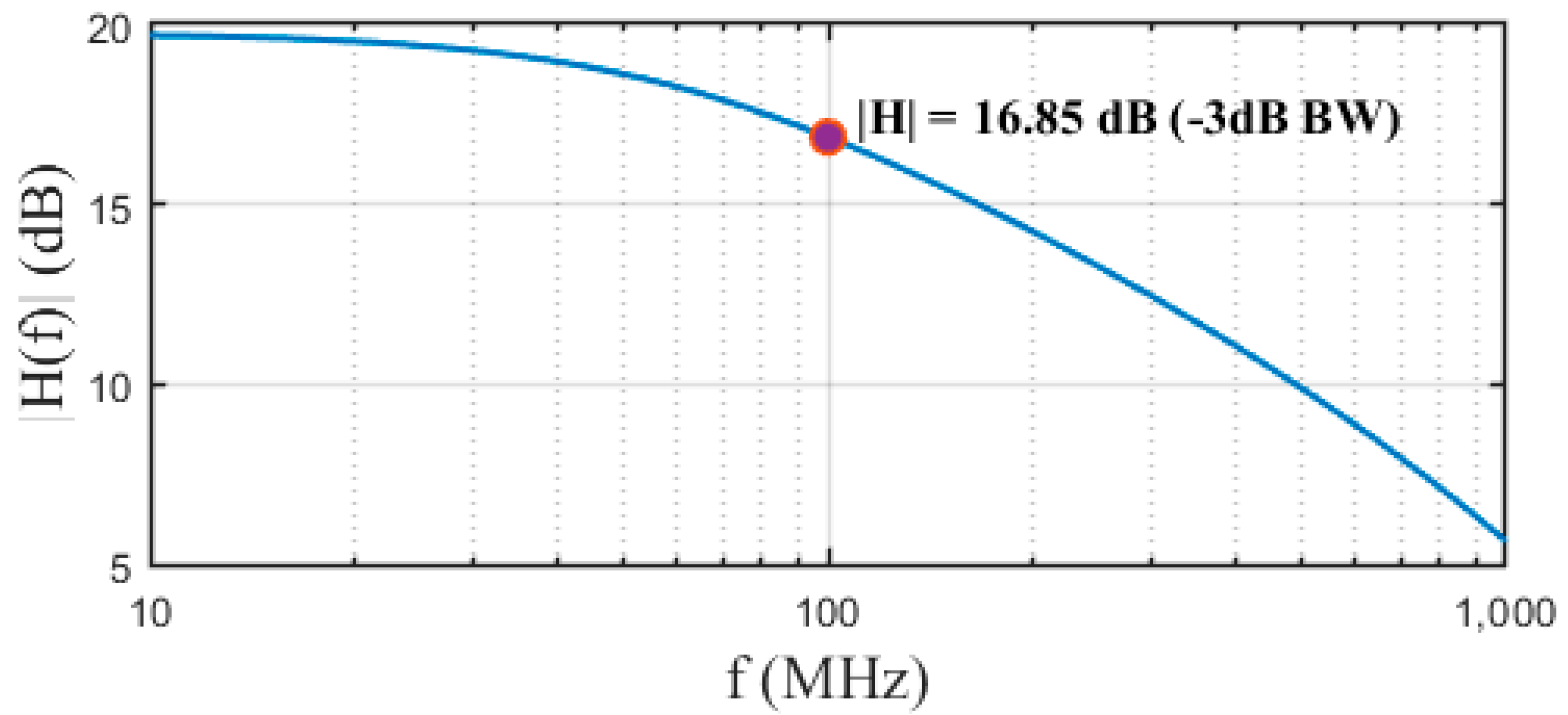
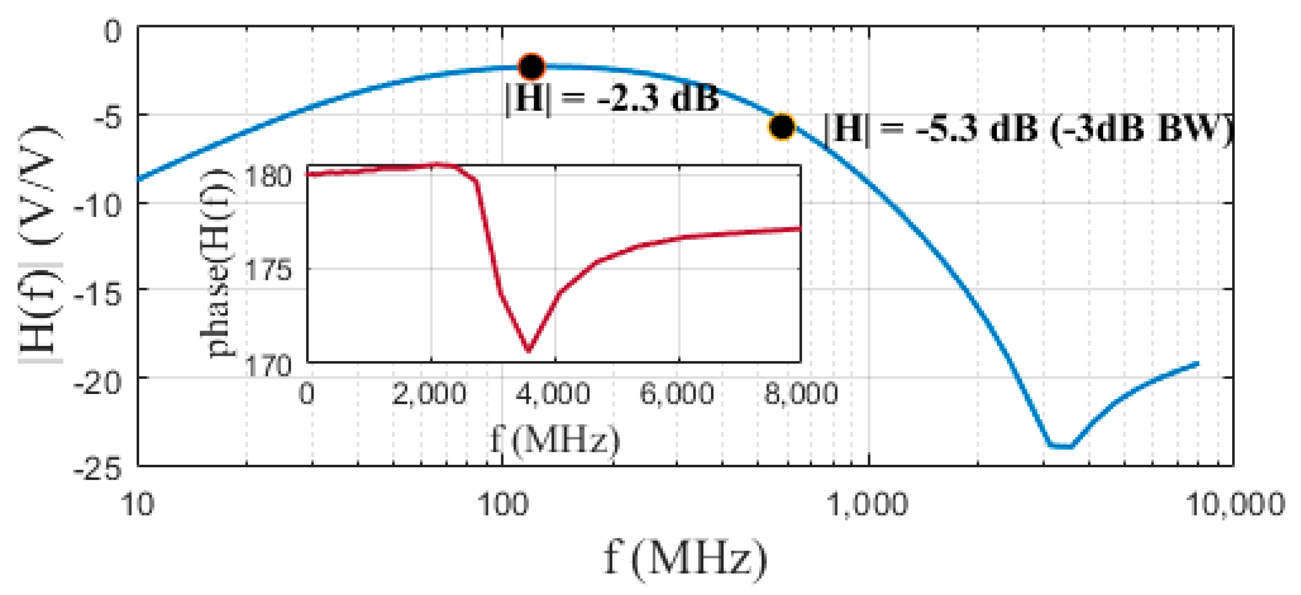
- Design an LPF (the simplest and with the smallest possible area) whose 3-dB bandwidth, BWLPF, is fIF, and with a minimum loss in the transfer magnitude, LossLPF.
- STEP 5.
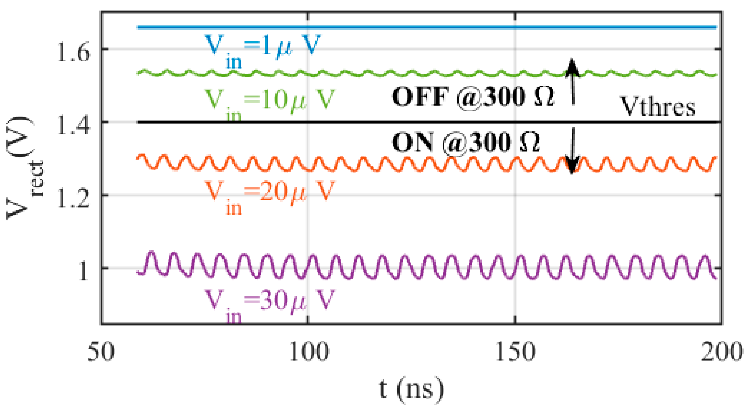
- In parallel, design an Envelope Detector whose output DC voltage, VoED_DC, is proportional to its output input and VoED_DCOFF − VoED_DCON| > Vdetect_min. The envelope detector fixes a minimum input voltage Vin_EDmin.
- STEP 6.
- With the information found in STEP 4 and STEP 5, design an intermediate-frequency amplifier IF-AMP, with a gain higher than GIF_AMP = GFE − GLNA − CGMix + LossLPF. The RF-FE gain is defined as GFE = Vin_EDmin /VSHNOON. Now the design is finished.
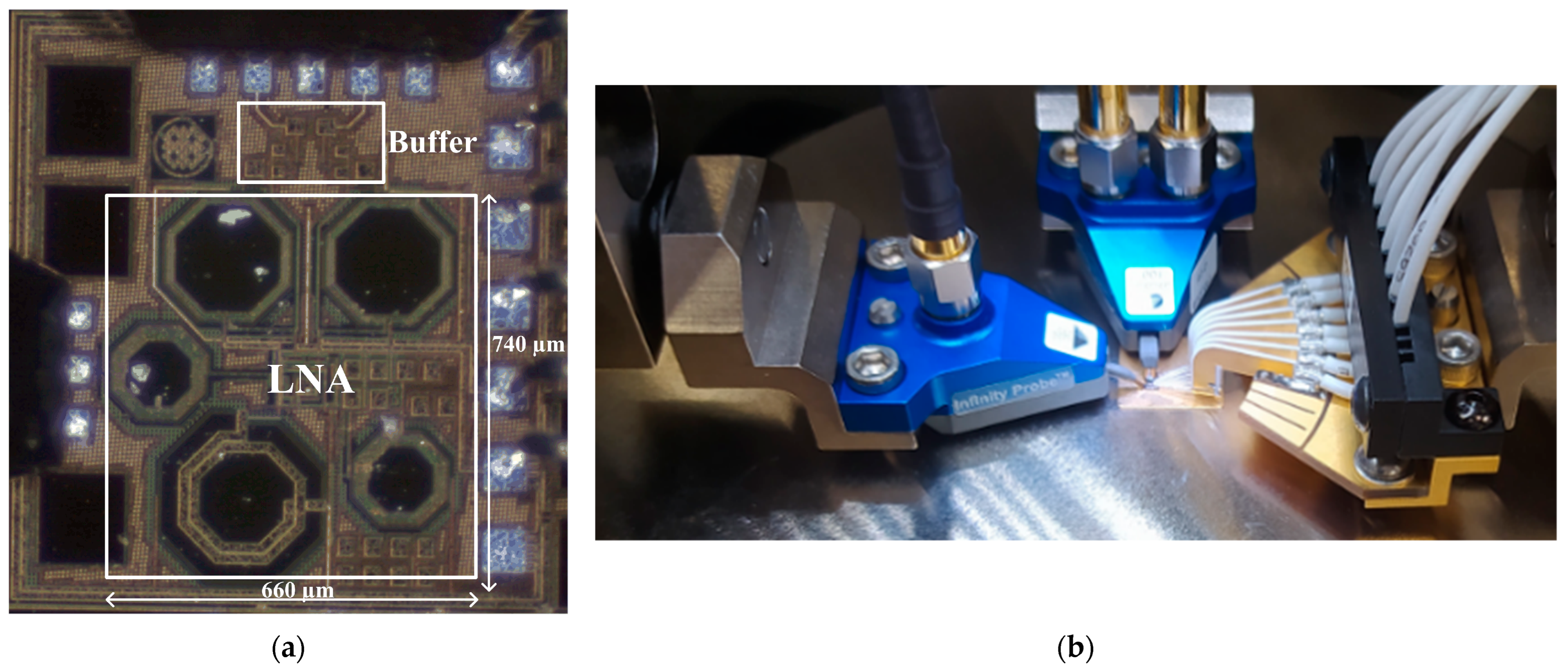
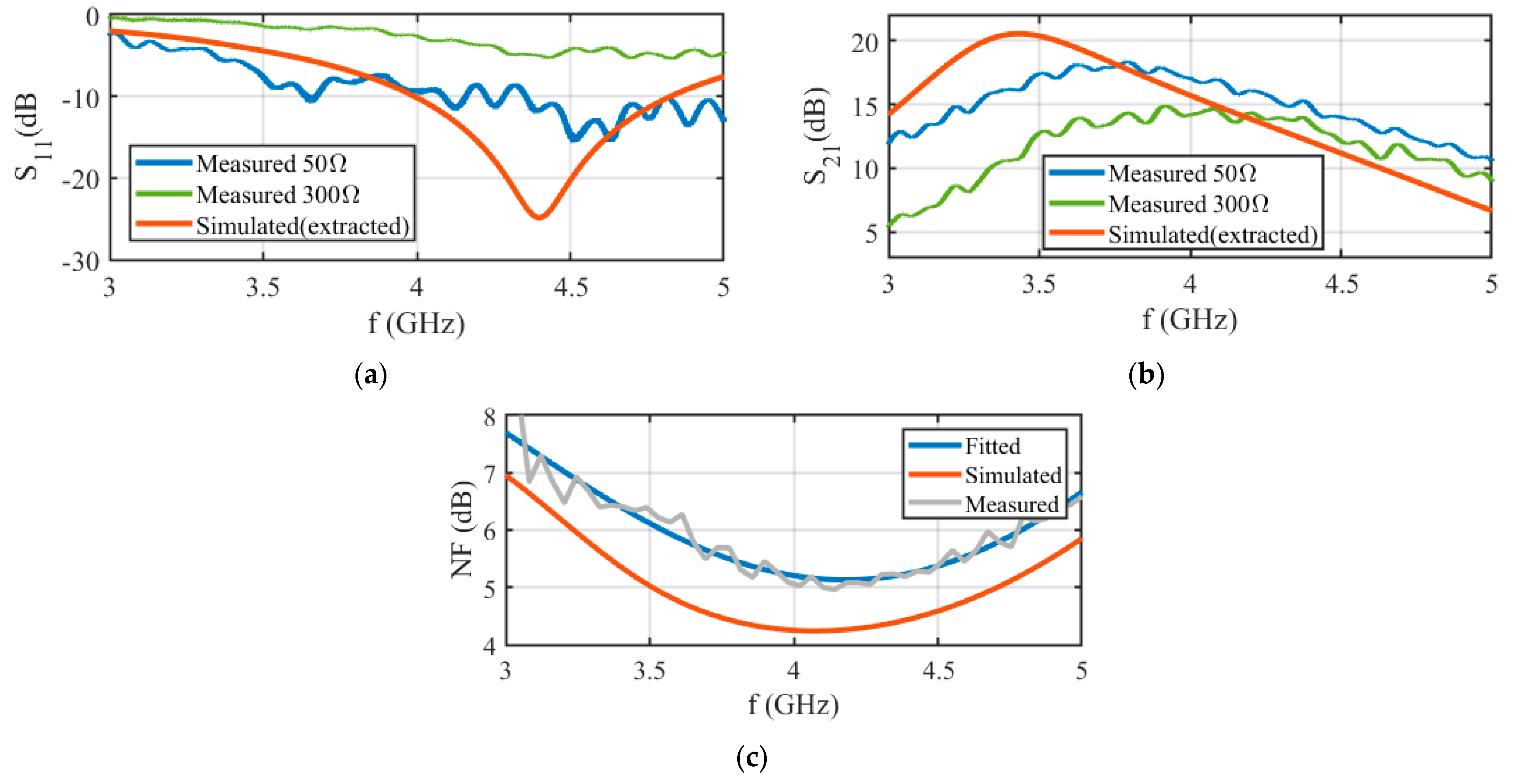
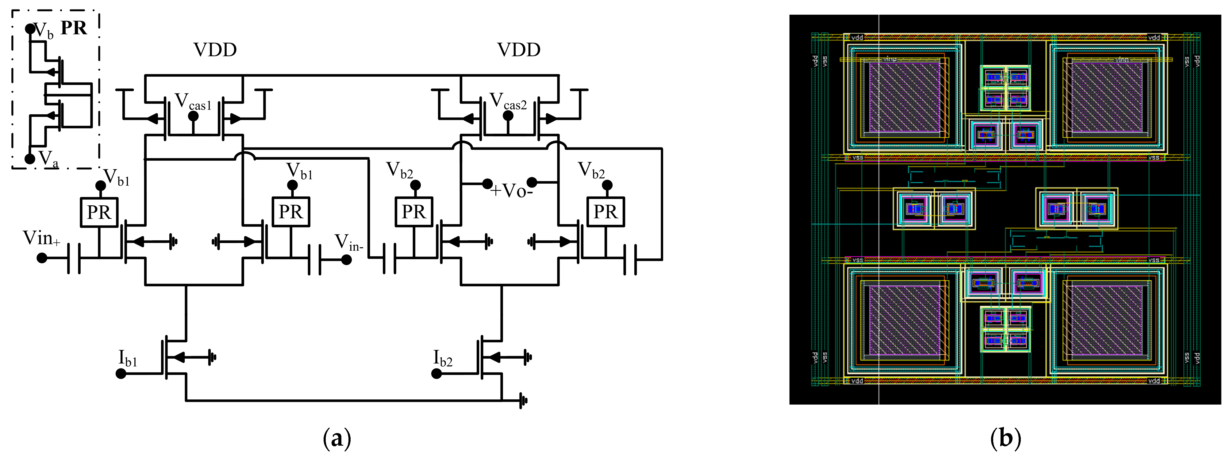
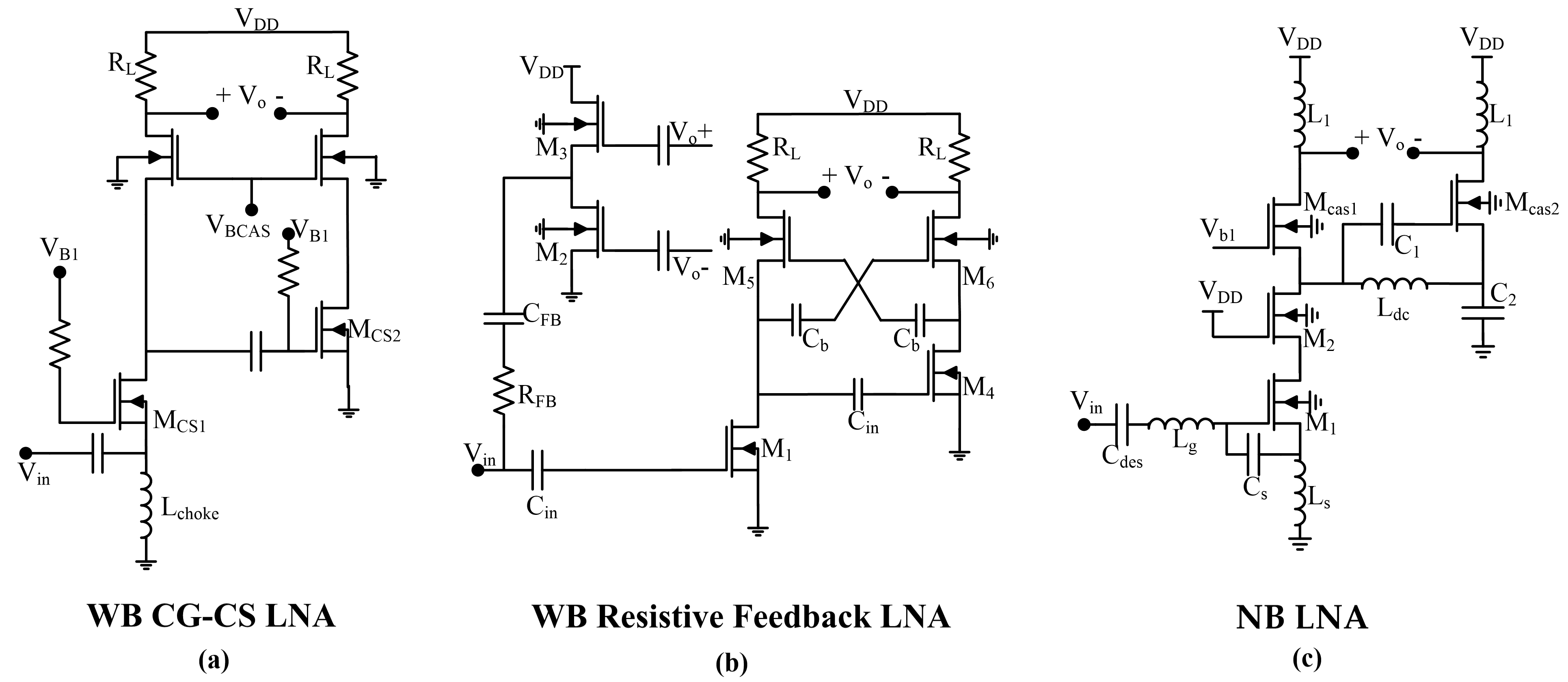
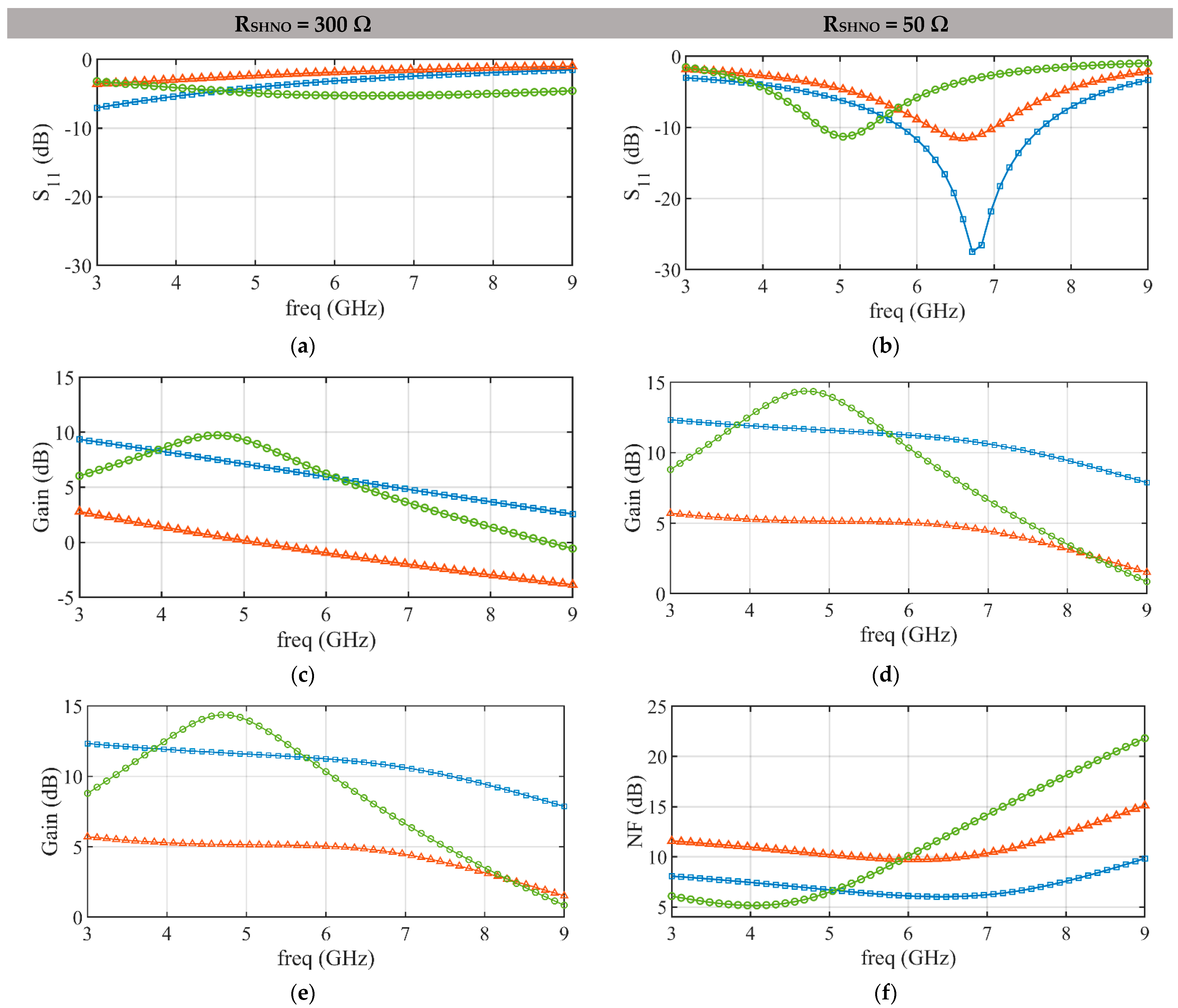
4.1. LNA
- Area: since p RF-FEs are needed, with p > 1 (see Figure 1), using NB-LNAs implies the take-up of a lot of silicon area due to passive inductors. WB-LNAs with no inductors occupy much less area.
- Input matching: since SHNO output impedance is far from (50 + 0j) Ω, input matching is better achieved in NB-LNAs due to inductors. Conversely, in WB-LNAs, the real part of the LNA input impedance Re(Zin) is generally adjusted using the input transistor connected in a common-gate fashion, being Re(Zin) ≅ 1/gm at low frequency. If there were no combination of transistor size and bias such that it generates a gm that gives a good return loss, the matching would be compromised.
- Gain: for WB-LNAs, their gain can be low because this is, generally, directly proportional to input transistor gm. Therefore, if ZSHNO is high, gm is low, and gain is reduced. For NB-LNAs, the inductor input matching network helps both to boost the gain and provides more degrees of freedom to achieve the matching.
- Noise Figure: Since improving matching and gain has a direct impact on noise reduction, it is expected that NB-LNAs have better noise figure than WB-LNAs.
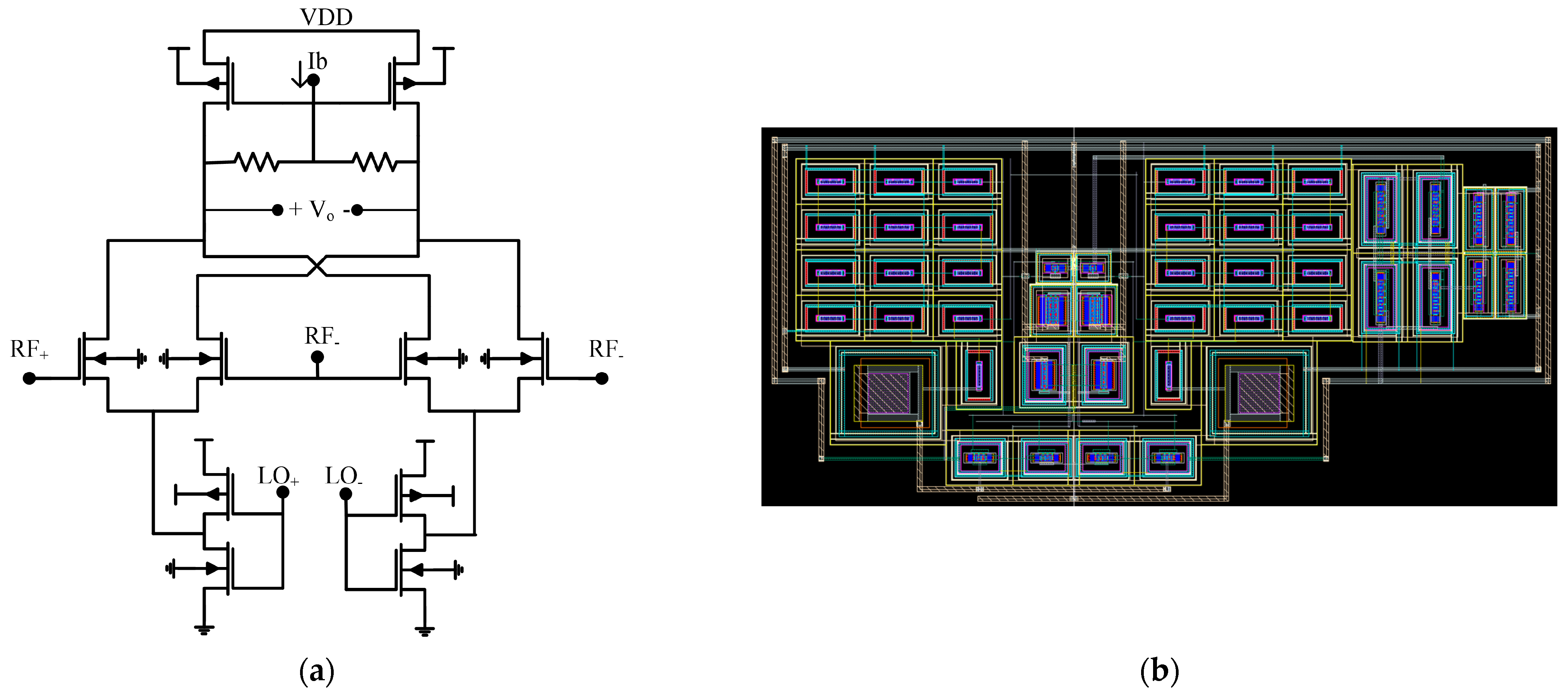
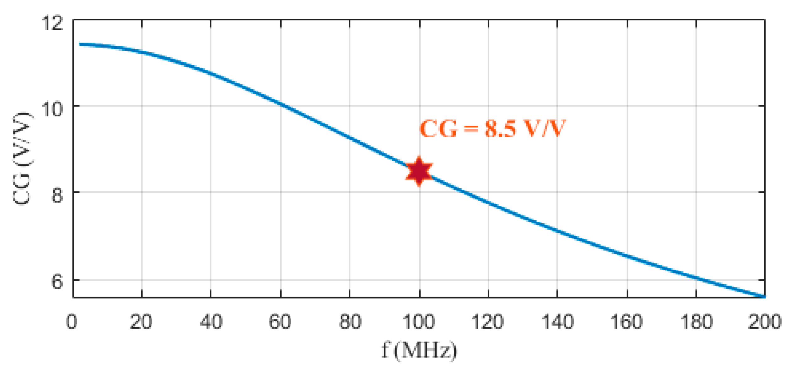
4.2. Mixer
4.3. Filter and Intermediate-Frequency Amplifier
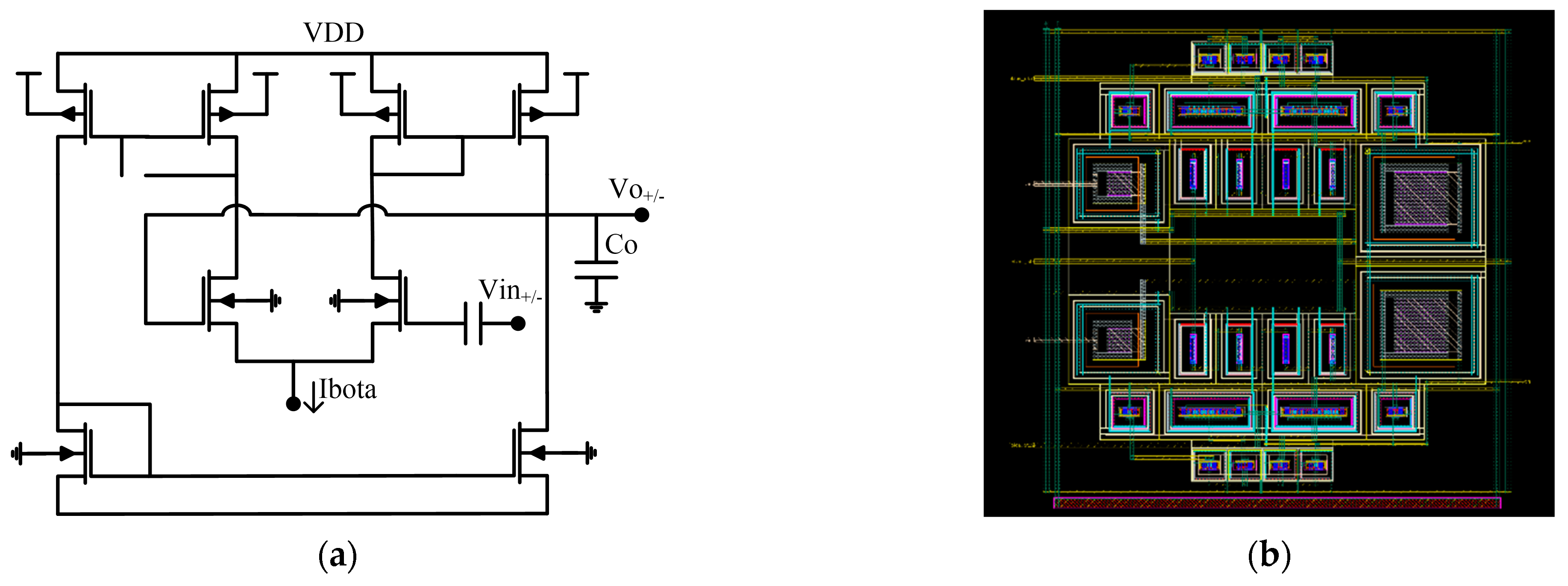
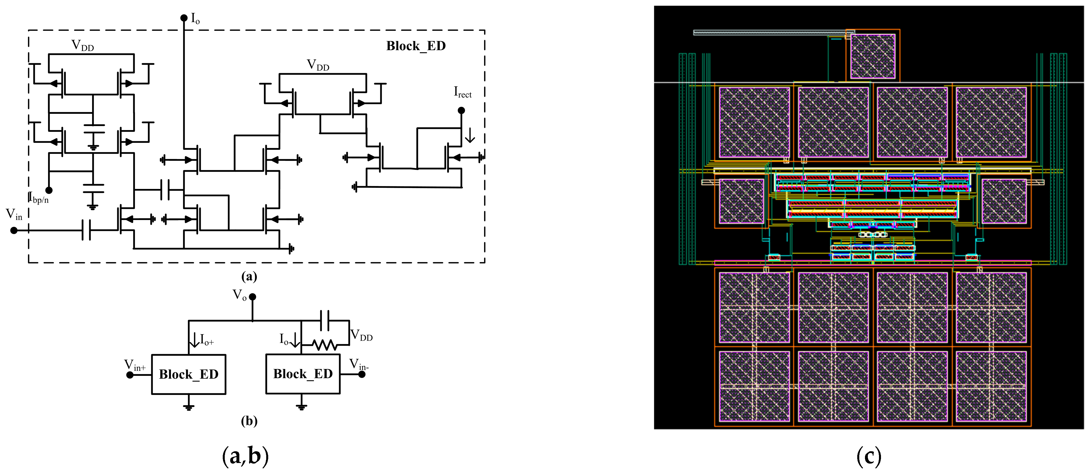
4.4. Envelope Detector
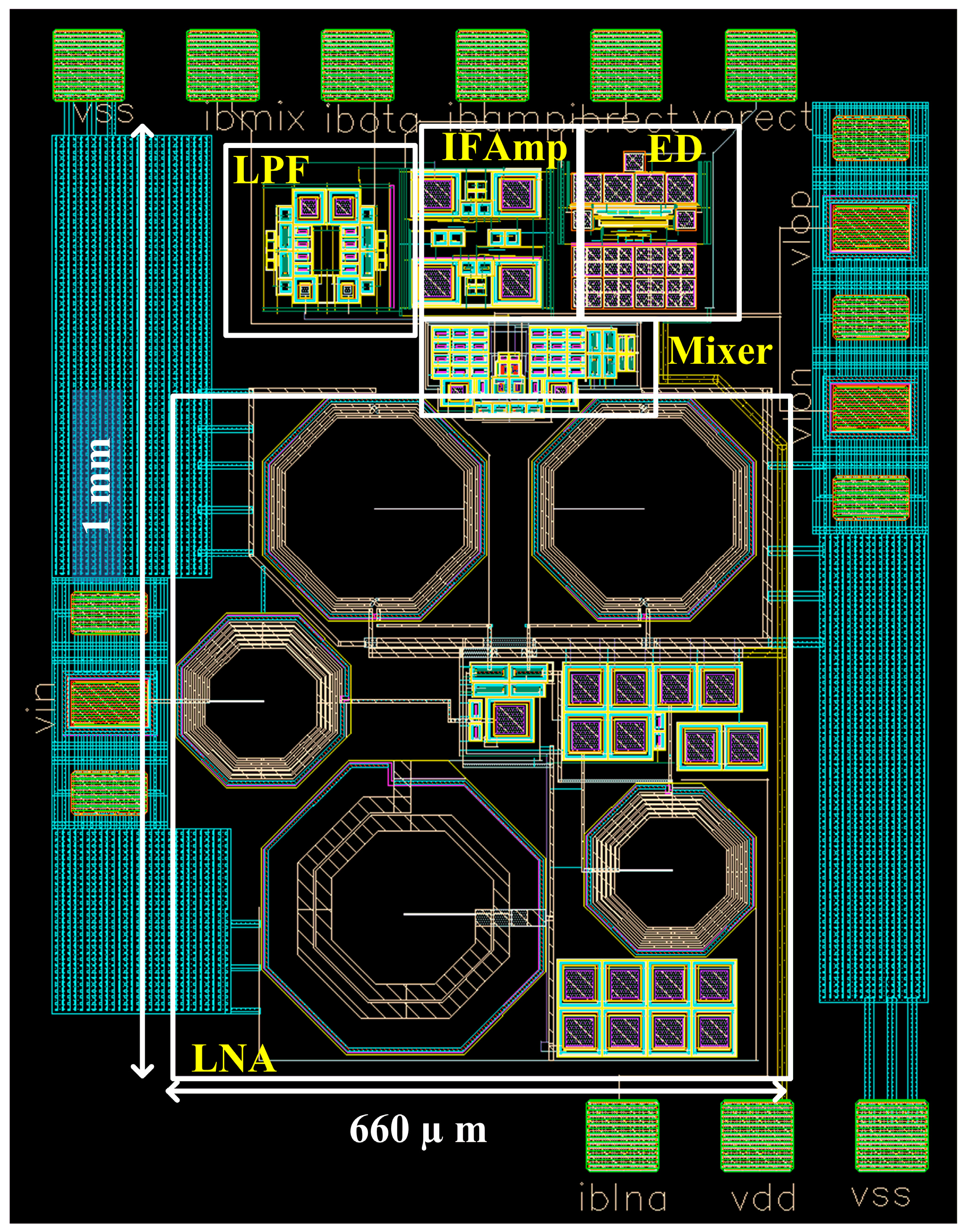
4.5. Complete FE Block
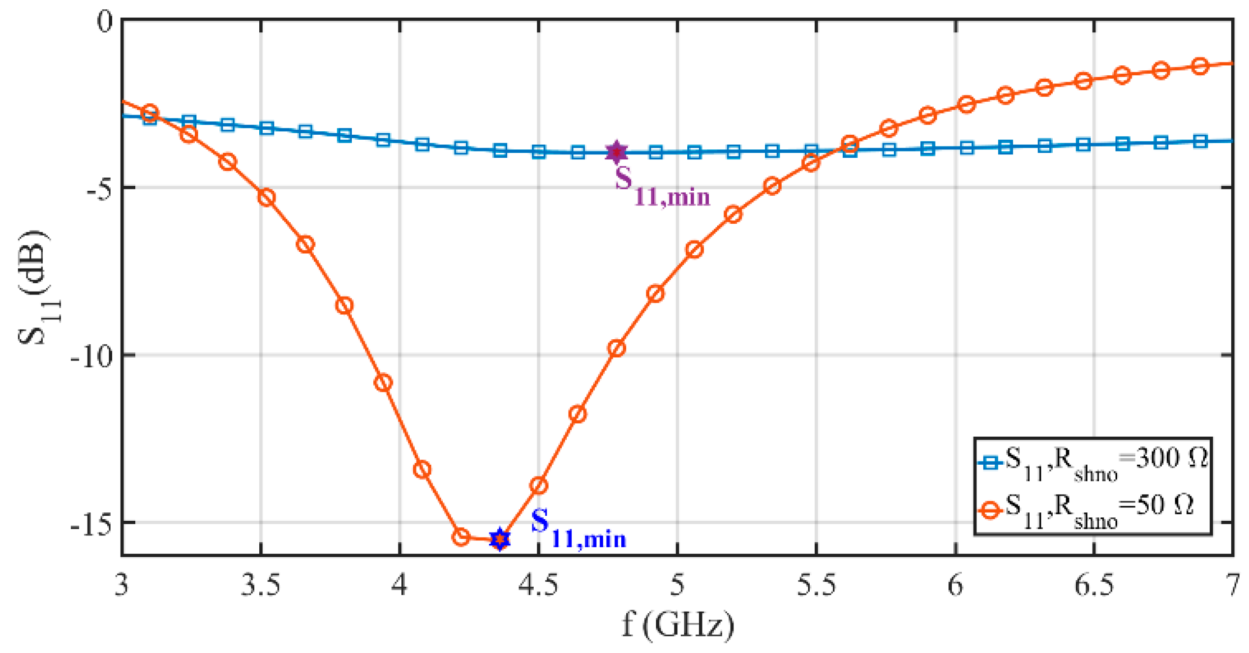
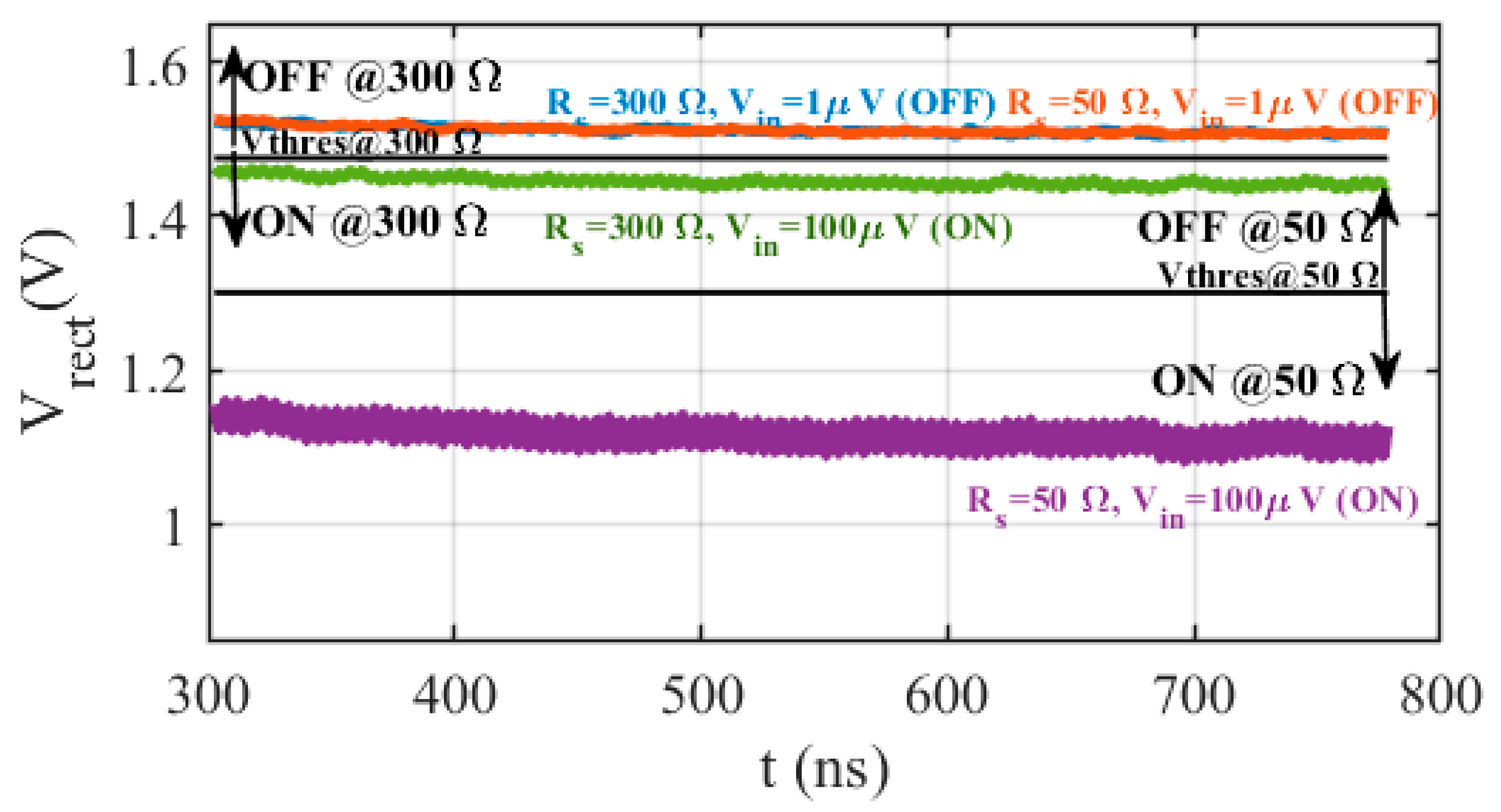
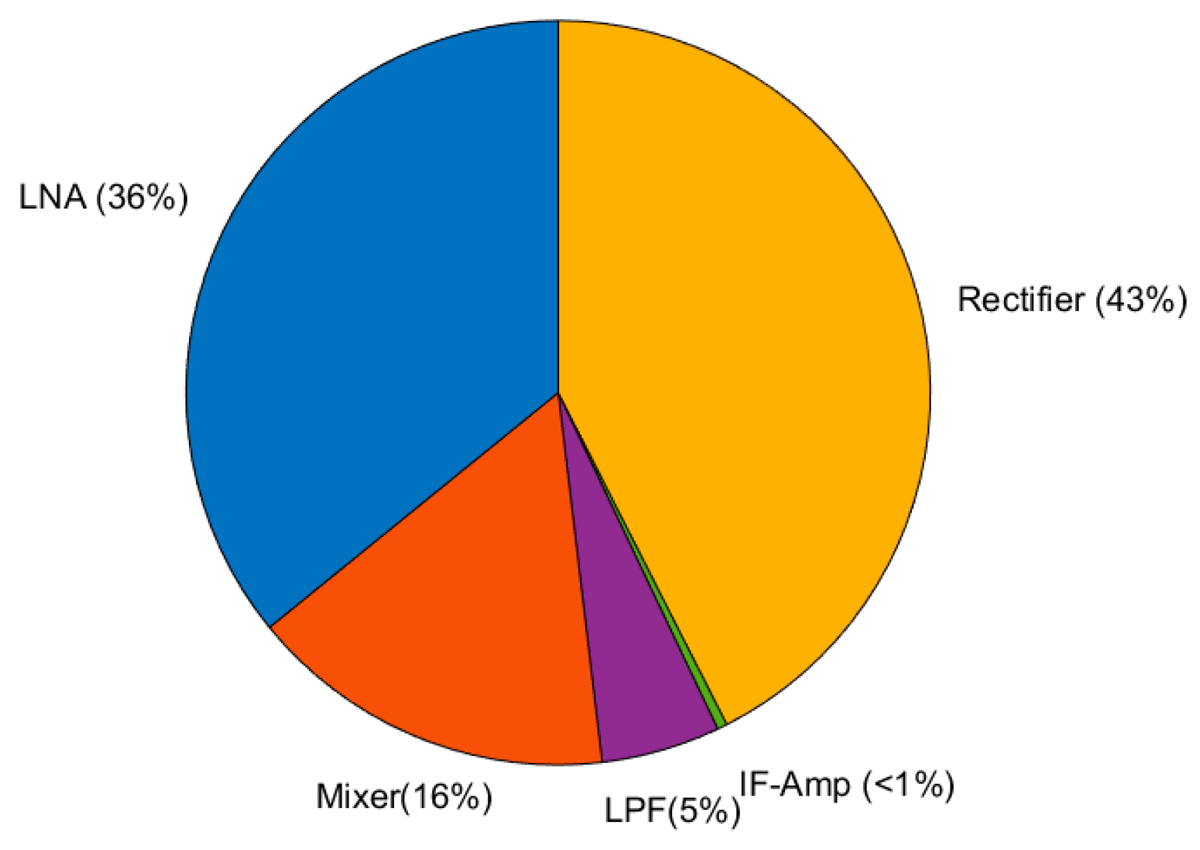
5. FE Results and Discussion
6. Conclusions and Future Work
Author Contributions
Funding
Data Availability Statement
Conflicts of Interest
References
- Tsunami of Data Could Consume one Fifth of Global Electricity by 2025|Environment|The Guardian. Available online: https://www.theguardian.com/environment/2017/dec/11/tsunami-of-data-could-consume-fifth-global-electricity-by-2025 (accessed on 3 March 2022).
- Mead, C. Neuromorphic Electronic Systems. Proc. IEEE 1990, 78, 1629–1636. [Google Scholar] [CrossRef] [Green Version]
- Human Brain Project Home. Available online: https://www.humanbrainproject.eu/en/ (accessed on 3 March 2022).
- Research Groups: APT—Advanced Processor Technologies (School of Computer Science—The University of Manchester). Available online: http://apt.cs.manchester.ac.uk/projects/SpiNNaker/project/ (accessed on 3 March 2022).
- Awad, A.A.; Dürrenfeld, P.; Houshang, A.; Dvornik, M.; Iacocca, E.; Dumas, R.K.; Åkerman, J. Long-range mutual synchronization of spin Hall nano-oscillators. Nat. Phys. 2016, 13, 292–299. [Google Scholar] [CrossRef]
- Demidov, V.E.; Urazhdin, S.; Ulrichs, H.; Tiberkevych, V.; Slavin, A.; Baither, D.; Schmitz, G.; Demokritov, S.O. Magnetic nano-oscillator driven by pure spin current. Nat. Mater. 2012, 11, 1028–1031. [Google Scholar] [CrossRef] [PubMed]
- Demidov, V.E.; Urazhdin, S.; Zholud, A.; Sadovnikov, A.V.; Demokritov, S.O. Nanoconstriction-based spin-Hall nano-oscillator. Appl. Phys. Lett. 2014, 105, 172410. [Google Scholar] [CrossRef]
- Dürrenfeld, P.; Awad, A.A.; Houshang, A.; Dumas, R.K.; Åkerman, J. A 20 nm spin Hall nano-oscillator. Nanoscale 2017, 3, 1285–1291. [Google Scholar] [CrossRef]
- Kumar, A.; Rajabali, M.; González, V.H.; Zahedinejad, M.; Houshang, A.; Åkerman, J. Fabrication of voltage-gated spin Hall nano-oscillators. Nanoscale 2022, 14, 1432–1439. [Google Scholar] [CrossRef]
- Muralidhar, S.; Houshang, A.; Alemán, A.; Khymyn, R.; Awad, A.A.; Åkerman, J. Optothermal control of spin Hall nano-oscillators. Appl. Phys. Lett. 2022, 120, 262401. [Google Scholar] [CrossRef]
- Zahedinejad, M.; Awad, A.A.; Muralidhar, S.; Khymyn, R.; Fulara, H.; Mazraati, H.; Dvornik, M.; Åkerman, J. Two-dimensional mutually synchronized spin Hall nano-oscillator arrays for neuromorphic computing. Nat. Nanotechnol. 2020, 15, 47–52. [Google Scholar] [CrossRef]
- Tarequzzaman, M.; Böhnert, T.; Decker, M.; Costa, J.D.; Borme, J.; Lacoste, B.; Paz, E.; Jenkins, A.S.; Serrano-Guisan, S.; Back, C.H.; et al. Spin torque nano-oscillator driven by combined spin injection from tunneling and spin Hall current. Commun. Phys. 2019, 2, 20. [Google Scholar] [CrossRef] [Green Version]
- Zahedinejad, M.; Mazraati, H.; Fulara, H.; Yue, J.; Jiang, S.; Awad, A.A.; Akerman, J. CMOS compatible W/CoFeB/MgO spin Hall nano-oscillators with wide frequency tunability. Appl. Phys. Lett. 2018, 112, 132404. [Google Scholar] [CrossRef]
- Romera, M.; Talatchian, P.; Tsunegi, S.; Araujo, F.A.; Cros, V.; Bortolotti, P.; Trastoy, J.; Yakushiji, K.; Fukushima, A.; Kubota, H.; et al. Vowel recognition with four coupled spin-torque nano-oscillators. Nature 2018, 563, 230–234. [Google Scholar] [CrossRef] [PubMed] [Green Version]
- Houshang, A.; Zahedinejad, M.; Muralidhar, S.; Chęciński, J.; Khymyn, R.; Rajabali, M.; Fulara, H.; Awad, A.A.; Dvornik, M.; Åkerman, J. Phase-Binarized Spin Hall Nano-Oscillator Arrays: Towards Spin Hall Ising Machines. Phys. Rev. Appl. 2022, 17, 014003. [Google Scholar] [CrossRef]
- Zahedinejad, M.; Fulara, H.; Khymyn, R.; Houshang, A.; Dvornik, M.; Fukami, S.; Kanai, S.; Ohno, H.; Åkerman, J. Memristive control of mutual spin Hall nano-oscillator synchronization for neuromorphic computing. Nat. Mater. 2021, 21, 81–87. [Google Scholar] [CrossRef]
- Leroux, N.; De Riz, A.; Sanz-Hernández, D.; Marković, D.; Mizrahi, A.; Grollier, J. Convolutional neural networks with radio-frequency spintronic nano-devices. Neuromorphic Comput. Eng. 2022, 2, 034002. [Google Scholar] [CrossRef]
- Ding, S.; Wang, N.; Bao, H.; Chen, B.; Wu, H.; Xu, Q. Memristor synapse-coupled piecewise-linear simplified Hopfield neural network: Dynamics analysis and circuit implementation. Chaos Solitons Fractals 2023, 166, 112899. [Google Scholar] [CrossRef]
- Fulara, H.; Zahedinejad, M.; Khymyn, R.; Awad, A.A.; Muralidhar, S.; Dvornik, M.; Akerman, J. Spin-orbit torque–driven propagating spin waves. Sci. Adv. 2019, 5, 9. [Google Scholar] [CrossRef] [PubMed] [Green Version]
- Ginés, A.; Fiorelli, R.; Villeagas, A.; Doldan, R.; Barragan, M.; Vazquez, D.; Rueda, A. Design of an Energy-Efficient ZigBee Transceiver, in Mixed-Signal Circuits; CRC Press: Boca Raton, FL, USA, 2018; pp. 192–223. [Google Scholar] [CrossRef]
- Razavi, B. RF MICROELECTRONICS, 2nd ed.; Prentice Hall: Hoboken, NJ, USA, 2011. [Google Scholar]
- Bagheri, R.; Mirzaei, A.; Chehrazi, S.; Heidari, M.E.; Lee, M.; Mikhemar, M.; Tang, W.; Abidi, A.A. An 800-MHz—6-GHz Software-Defined Wireless Receiver in 90-nm CMOS. IEEE J. Solid-State Circuits 2006, 41, 2860–2876. [Google Scholar] [CrossRef]
- Im, D.; Nam, I.; Lee, K. A CMOS active feedback balun-LNA with high IIP2 for wideband digital TV receivers. IEEE Trans. Microw. Theory Tech. 2010, 58, 3566–3579. [Google Scholar] [CrossRef]
- Ji, Y.; Wang, C.; Liu, J.; Liao, H. 1.8dB NF 3.6mW CMOS active balun low noise amplifier for GPS. Electron. Lett. 2010, 46, 251–252. [Google Scholar] [CrossRef]
- Fiorelli, R.; Silveira, F.; Peralías, E. MOST moderate-weak-inversion region as the optimum design zone for CMOS 2.4-GHz CS-LNAs. IEEE Trans. Microw. Theory Tech. 2014, 62, 556–566. [Google Scholar] [CrossRef] [Green Version]
- Fiorelli, R.; Silveira, F. Common gate LNA design space exploration in all inversion regions. In Proceedings of the 2008 Argentine School of Micro-Nanoelectronics, Technology and Applications, Buenos Aires, Argentina, 18–19 September 2008. [Google Scholar]
- Fiorelli, R.; Peralías, E. Semi-empirical RF MOST model for CMOS 65 nm technologies: Theory, extraction method and validation. Integration 2016, 52, 228–236. [Google Scholar] [CrossRef] [Green Version]
- Klumperink, E.; Louwsma, S.; Wienk, G.; Nauta, B. A CMOS switched transconductor mixer. IEEE J. Solid-State Circuits 2004, 39, 1231–1240. [Google Scholar] [CrossRef] [Green Version]
- Fiorelli, R.; Villegas, A.; Peralias, E.; Vazquez, D.; Rueda, A. 2.4-GHz single-ended input low-power low-voltage active front-end for ZigBee applications in 90 nm CMOS. In Proceedings of the 2011 20th European Conference on Circuit Theory and Design (ECCTD), Linköping, Sweden, 29–31 August 2011; pp. 829–832. [Google Scholar] [CrossRef] [Green Version]
- Deliyannis, T.; Sun, Y.; Fidler, J. Continuous-Time Active Filter Design; CRC Press: Boca Raton, FL, USA, 2019. [Google Scholar] [CrossRef]
- Xia, J.; Boumaiza, S. A Novel Broadband Linear-in-Magnitude RF Envelope Detector With Enhanced Detection Speed and Accuracy. IEEE Microw. Wirel. Compon. Lett. 2015, 25, 325–327. [Google Scholar] [CrossRef]


Disclaimer/Publisher’s Note: The statements, opinions and data contained in all publications are solely those of the individual author(s) and contributor(s) and not of MDPI and/or the editor(s). MDPI and/or the editor(s) disclaim responsibility for any injury to people or property resulting from any ideas, methods, instructions or products referred to in the content. |
© 2023 by the authors. Licensee MDPI, Basel, Switzerland. This article is an open access article distributed under the terms and conditions of the Creative Commons Attribution (CC BY) license (https://creativecommons.org/licenses/by/4.0/).
Share and Cite
Fiorelli, R.; Peralías, E.; Méndez-Romero, R.; Rajabali, M.; Kumar, A.; Zahedinejad, M.; Åkerman, J.; Moradi, F.; Serrano-Gotarredona, T.; Linares-Barranco, B. CMOS Front End for Interfacing Spin-Hall Nano-Oscillators for Neuromorphic Computing in the GHz Range. Electronics 2023, 12, 230. https://doi.org/10.3390/electronics12010230
Fiorelli R, Peralías E, Méndez-Romero R, Rajabali M, Kumar A, Zahedinejad M, Åkerman J, Moradi F, Serrano-Gotarredona T, Linares-Barranco B. CMOS Front End for Interfacing Spin-Hall Nano-Oscillators for Neuromorphic Computing in the GHz Range. Electronics. 2023; 12(1):230. https://doi.org/10.3390/electronics12010230
Chicago/Turabian StyleFiorelli, Rafaella, Eduardo Peralías, Roberto Méndez-Romero, Mona Rajabali, Akash Kumar, Mohammad Zahedinejad, Johan Åkerman, Farshad Moradi, Teresa Serrano-Gotarredona, and Bernabé Linares-Barranco. 2023. "CMOS Front End for Interfacing Spin-Hall Nano-Oscillators for Neuromorphic Computing in the GHz Range" Electronics 12, no. 1: 230. https://doi.org/10.3390/electronics12010230