
A Compact W-Band Low-Noise Radiometry Sensor for a Single-Pixel Passive Millimeter-Wave Imager

1
Department of Electronics and Communications Engineering, Kocaeli University, Kocaeli 41001, Turkey
2
Department of Electrics and Electronics Engineering, Karamanoglu MehmetBey University, Karaman 70200, Turkey
*
Author to whom correspondence should be addressed.
Electronics 2023, 12(10), 2330; https://doi.org/10.3390/electronics12102330
Submission received: 1 April 2023
/
Revised: 16 May 2023
/
Accepted: 18 May 2023
/
Published: 22 May 2023
(This article belongs to the Special Issue Recent Advances in Micro/Millimeter-Wave Imaging Technology)
Abstract
:Recently, studies on the remote detection of dangerous objects on the person have gained importance with increased security problems. Therefore, the use of passive millimeter waves in security systems is increasing because they are harmless to health and can penetrate clothes. In this study, a compact low-noise radiometric sensor (LNRS) that can be used to view hidden objects on the person was constructed. The LNRS can be arrayed thanks to its small size and ease of use, and can be used in imaging applications thanks to the 0.24 K resolution obtained. In addition, a passive millimeter imaging system (PMMWI) was developed to obtain images with the LNRS. The PMMWI system, which is realized in a quasi-optical structure, can be used in many experimental studies thanks to its compact structure.
1. Introduction
Due to the increasing security needs worldwide, studies on remote sensing are increasing. In particular, studies on remote sensing systems are gaining importance. Today, the focus is on remote sensing systems of hidden objects hidden on the person; these are used in places where people enter and exit, such as airports, train stations, schools, and shopping centers. One of the technologies used in these systems is imaging systems with millimeter-wave passive radiometry receivers [1].
Any object with a temperature other than absolute zero can emit millimeter waves. The strength of the propagating wave depends on the temperature of the object and its emissivity. Millimeter waves penetrate clothing, non-metallic objects, and foggy, cloudy environments. Due to this feature, millimeter-wave receivers can be used in imaging systems. Systems that perform imaging at millimeter-wave frequencies using the natural propagation of objects are called millimeter-wave passive imaging systems (PMMWI). These systems are structures that obtain images by collecting electromagnetic waves emitted from objects using sensitive radiometric receivers. These systems are passive as they use natural electromagnetic waves emitted from objects [2,3]. Although the image quality is relatively low compared to other systems (backscatter X-ray and active millimeter wave), the main advantage of PMMWIs is that they do not cause any harm to human health since they are not broadcast. They can also display from a longer (safe) distance (standoff distance) [4]. In addition, a PMMWI can be hidden and display larger areas and moving people.
Studies about PMMWI systems became even more prominent in the late 1990s with the development of monolithic microwave integrated circuit (MMIC) based LNAs (low-noise amplifiers) at 100 GHz frequencies [5]. First, millimeter-wave imagers started to be developed in 1996 when Lockheed Martin Company obtained images of weapons under clothing with a single-pixel PMMWI with 0.4 K sensitivity [6]. After this date, commercial PMMWI systems continued to be developed in various structures for security applications, remote sensing, and metrology systems [7].
In the studies carried out to date, PMMWI has been performed with a receiver that converts frequency down-conversion with a sub-harmonic mixer at a frequency of 0.2 THz [8]. In such receivers, the hardware is more complex and costly as it requires a LO (local oscillator) and is unsuitable for stringing. There are PMMWI systems in which active and passive receivers are used. Although these systems are advantageous in terms of increasing image quality and detection, they bring hardware complexity and a signal processing burden to the system with software. In a study performed by [9], PMMWI commercial devices use receivers operating between 30 GHz and 35 GHz. Image processing algorithms increase the image resolution due to the frequency band. Although some systems use passive receiver arrays, they require an active source for imaging [10]. There are single-chip receivers in the MMIC structure [11]. Although compact receivers can be realized with such MMICs, these integrated circuits (IC) need external LO because they are super-heterodyne [12]. In [13], image processing algorithms are used to increase the image quality of the imaging system using a 35 GHz frequency receiver.
There are systems using bolometers as sensors. Bolometer detectors used at millimeter-wave (mmW) frequencies are not in commercial production yet, and cooling of the detectors is one of the biggest obstacles to their use [14,15]. Direct diode detection receivers have a wide operating frequency band, and therefore a high thermal resolution [16]. Thus, they improve the image quality of the PMMWI in which they are used. However, they have not yet been produced commercially, so PMMWI applications are limited and have the disadvantage of requiring an external signal/noise source for long-range imaging. Today, receiver detector ICs produced with the antenna are at the prototype stage [17]. The fact that this type of detector is not yet commercially available and requires complex circuits to perform PMMWI makes it challenging to use.
According to the literature review, it has been seen that the studies on performing PMMWI, in general, are studies on hardware development, and software and image processing algorithms. Using image processing algorithms with software imposes a software processing load on the system. Hardware development has focused on using different receiver topologies and next-generation semiconductor sensor technologies. Such studies not only improve image quality but also bring hardware complexity and complicate reproducibility. Considering all these studies, it is possible to summarize the main objectives of this study as follows:
- Despite using the known preamplifier total power receiver topology, the receiver is equipped with new-generation LNA MMICs with low-noise figures.
- Zero bias Schottky diode structure is used as a detector with the LNA in the receiver. Thus, a compact receiver structure was obtained.
- The receiver structure is designed with a waveguide output so that a different antenna or LNA can be added to the front when necessary.
2. Materials and Methods
A typical optical imaging system is given in Figure 1. Briefly, the operation of this optical system makes use of the rays emanating from the target, which are directed onto the optical sensor array through the optical lens. The image obtained in the sensor is recorded. Similarly, using an optic assembly and sensor, a PMMWI system is obtained when it operates at millimeter-wave frequencies.
All natural objects with an absolute temperature above zero emit electromagnetic radiation. According to Planck’s law, a blackbody radiates uniformly in all directions with a spectral energy density of Eλ [18].
Here, is frequency, is the absolute temperature of the radiating object in Kelvin, Planck constant , is the Boltzmann constant , and is the speed of light (2.9979 × 10⁸ m·s−1).
In the low-frequency region, Plank’s law tends to Rayleigh–Jeans approximation. In addition, the ratio of the radiation emitted from natural objects to the radiation emitted from a blackbody with a similar surface is called emissivity (ε) and is between 0 and 1. In this case, every material with a temperature different from absolute zero radiates in proportion to its emissivity value. According to these explanations, Equation (1) can be written with f as the center frequency and Δf as the bandwidth, as follows [19]:
Thus, all objects radiate depending on their temperature and emissivity ratio. Systems that measure the part of the radiation of the objects in the mmW spectrum and display accordingly are called PMMWI. For this reason, dangerous substances may be viewed from a safe distance according to the radiation intensity [20].
In general, the PMMWI consists of three main components. These components are the low-noise receiver sensor (LNRS), the semi-optical imaging (QOI) system, and the control and data acquisition units that control both systems.
The system diagram is given in Figure 2. In this study, a single-pixel PMMWI and a low-cost, mmW W-band (94 GHz center frequency and 10 GHz bandwidth) LNRS to be used in this system will be implemented. Thanks to the QOI, a virtual image is created with the signals emitted from the target. Then, the power density of this image is converted to an electric signal with LNRS to obtain an image.
2.1. Low-Noise Radiometric Receiver Sensor (LNRS)
Ideally, as shown in Figure 3, the LNRS is expected to receive all the electromagnetic energy emitted from a radiating object. Thus, the power value of the emitted energy is measured by LNRS and used in imaging.
In the actual case, like every electronic circuit, LNRSs have gain value, operating bandwidth, and noise values they create. An LNRS with an electronic circuit can be modeled as in Figure 4. Here, k is the Boltzmann constant (, G is the receiver gain, B is the receiver operating bandwidth, P is the receiver output power (Watts), TA is the receiver antenna temperature (K), and TN is the receiver temperature (K).
In this case, the sensitivity of the LNRS depends on the transfer of the TA variation from its input to its output in such a meaningful way that it can be measured (resolution) and is denoted by ΔT. Here, t is the integration time (seconds) and can be defined as the data sample holding of the system.
Electronically realizable LNRS structures and some of their important features that have emerged mostly since the 2000s, as a result of MMIC (monolithic microwave integrated circuit) technology developments and increasing commercial applications, are given in Table 1.
When Table 1 is examined, three basic receiver structures can be seen for the LNRS design that can be created with components and MMIC (Bolometer structures are not yet available on a component basis). A direct sensing structure with a preamplifier was chosen for LNRS in terms of resolution, cost, and high output signal power for imaging. This structure contains an LNA and a detector diode. The most crucial design step is determining the MMIC, LNA, and detector parameters used in the LNRS structure. Equation (3) is used to determine the LNRS parameters. For this purpose, preliminary analyses were carried out for an ambient temperature of 293 K (20 ). Here, the relative status of B, τ, TA, and TN parameters is examined. TN is expressed as the receiver temperature and is a function of the receiver noise value (). is the linear value of the noise figure () ( = 10Log()). Components such as the receiver and LNA are usually given the NF value. In this case, TN = ambient temperature (K) × (F − 1).
The resolution value obtained in Figure 5 is shown with the green area. Accordingly, for the first analysis, the design can be determined as B > 10 GHz, τ ≥ 1 ms, and NF < 4 dB.
Especially in recent years, the development of automobile RADARs, E-band communication systems, and mmW 5 G systems have increased MMIC production and the number of manufacturers in these frequencies. OMMIC’s CGY2190UH/C2 MMIC was used as the LNA to achieve the above design values for the LNRS. The CGY2190UH/C2 is a four-stage low-noise amplifier with a wide frequency range: 75–110 GHz and 23 dB small signal gain with an exceptionally low-noise figure of 2.8 dB at 90 GHz combined with ultra-low power consumption (drain voltage (Vd) = 1 V, gate voltage (Vg) = 0 V, total drain current = 33 mA). The MMIC is manufactured using OMMIC’s advanced proprietary 70 nm MHEMT technology [22]. The CGY2870AUH/C1 zero bias detector diode of the same company was used as the detector. The CGY2870AUH/C1 is a high-performance GaAs 50 Ohms matched zero bias detector diode operating as high as W-band. As a detector diode, the CGY2870AUH/C1 has a sensitivity of 8.5 mV/µW at 100 GHz and noise equivalent power (NEP) of 11 pW/√Hz [23]. In this case, the LNRS and the MMIC mentioned above, the LNA, and the diode detector enabled these circuits to work. In addition, it has an input interface where power and DC circuits and antennas can be connected in the W-band. The LNRS block structure is given in Figure 6.
Brass was chosen for the LNRS case because it can be easily shaped by machining and can be coated with gold directly through electroplating. The gold plating was preferred due to the increased conductivity of the case surface and its corrosion resistance. An LNRS consists of 3 parts: brass case, direct current (DC) circuit part, and mmW circuit part. A DC supply connector and signal output connector are mounted on the brass case. An mmW signal input is made with waveguide input in Wr-10 UG387/U-M flange standard so that W-band antennas can be connected. Since this waveguide is machined into case parts, it is present in its entirety. The inner dimensions of the WR-10 rectangular waveguide are 2.54 mm × 1.27 mm. The waveguide is terminated by bending 90° on the E plane from the entrance. The transition from the waveguide to the mmW circuit is provided by placing the probe with a microstrip (MS) line. The mmW circuit part comprises an MS probe, LNA, MS line, and detector, respectively. There are also the necessary single-layer capacitors (SLCs) for the LNA. These elements are mounted to the case with epoxy adhesive. Bond wires are used to connect to each other and the DC circuit.
Due to its low loss, a printed circuit board with a Rogers RO5880 [24] duroid dielectric layer is used as a substrate for the MS probe and MS line. The dielectric thickness of the board used is 127 um and the copper thickness is 8 um. The dielectric constant is 2.2 and the loss tangent is 0.0009. The MS probe is placed in the guide for the transition from the WR-10 waveguide to the MS line. The patch sizes on it are 0.68 mm × 0.65 mm and the impedance matching line connecting this patch to the 50 Ohm MS line is 0.20 mm × 0.35 mm. The line width of the 50 Ohm line is 0.39 mm. The WR-10 waveguide MS line transition structure and its sizes are shown in Figure 7. This structure was simulated in the 3D electromagnetic analysis software CST Microwave Studio. According to the simulation result, the transition loss (|S2|dB) in the operating frequency of the structure to be used is >0.3 dB. The simulation result is given in Figure 8. The MS probe circuit is mounted on the case surface with conductive epoxy adhesive.
The microstrip is attached to the casing surface after the line by sticking it with CGY2190UH/C2 MMIC LNA epoxy adhesive. The microstrip and LNA RF lines are connected by wire bonding with 25 um diameter gold wires. In addition, four parallel 47 pF single-layer capacitors are placed on both sides of the LNA between the drain and gate voltage lines and the case. A 50 Ohm MS line circuit is mounted behind the LNA. The CGY2870AUH/C1 detector is mounted after the line. The detector DC pad is connected to the input pad of the DC circuit part in the LNRS with a bond wire. Thus, the mmW circuit in the LNRS is completed.
The LNRS DC circuit, on the other hand, consists of the supply voltages required for the LNA and the circuits that filter and amplify the detector output signal. The supply voltage required for the operation of the system is 5 V DC and is taken with the chassis-mounted feed-thru connector. By using DC-to-DC converters, the necessary +4 V and −4 V DC voltages for the amplifier and filter circuit are obtained. The amplifier and low pass filter (LPF) were carried out with the operational amplifier. Amplifier gain and LPF cutoff frequency can be adjusted on the circuit with resistor and capacitor values. This study set the gain to 15 and the LPF cutoff frequency to 1 KHz. The filtered and amplified signal is transferred out of the case via the SMA female connector. In addition, the drain voltage required for the LNA (Vd = 1 V) was obtained using a DC-to-DC converter from +4 V voltage. This voltage was given to LNA drain pads via SLCs using bond wires over a FET (field effect transistor)-based switch. The gate voltage required for the LNA (Vg = −0.1 V) was obtained using a DC-to-DC converter from a −4 V voltage. This voltage was given to LNA gate pads over SLCs using bond wires. In addition, the drain switch was controlled with this DC-to-DC converter output, because the drain voltage must be given after the gate voltage for the LN to work. Otherwise, the LNA may be damaged. The LNRS electrical connection diagram is given in Figure 9.
The LNRS has a compact structure due to its dimensions of 20 mm × 20 mm × 85 mm (with SMA connector) and photographs of it are given in Figure 10.
2.2. Quasi-Optical Imaging System
Just as optical imaging systems need a lens or lens system to drop the image onto the sensor, the PMMWI system needs a quasi-optical imaging system to acquire images with LNRS. The quasi-optics system determines parameters such as viewing area, viewing distance, image area, and image resolution. The spatial resolution of the quasi-optical imaging system (s) according to the Rayleigh criterion is given in Equation (4). Here, R is the target distance, D is the diameter of the reflector or lens, and λ is the operating center frequency wavelength.
LNRS structures are more extensive compared to optical sensors. Therefore, creating two-dimensional (2D) arrays that take up much space is challenging. For this reason, quasi-optical imaging systems contain mechanisms that provide one- or two-dimensional movement together with an image-focusing element (lens or reflector mirror) to obtain images. Figure 11 shows the structure with a dielectric lens. Imaging is obtained by scanning the image formed between the lens with LNRS. In Figure 12, the system structure with reflector is shown. Here, the pre-focus or post-focus image is obtained by scanning with LNRS. In addition, the reflector systems themselves can obtain an image by scanning the target. Imaging systems containing dielectric lenses [25,26], imaging systems containing reflectors [27,28,29], and imaging systems containing both [30] have been presented in the literature. In order to obtain images with these systems, image or target scanning is performed with the 2D movement of the system, the movement of the sensor, and the system or the movement of the mirrors within the system.
In this study, a dielectric-lens-based quasi-optical imaging system, which can use a single LNRS and therefore scan in Cartesian coordinates, was constructed. The Quasi-optical imaging system consists of two main parts: a dielectric lens and a Cartesian scanner.
The dielectric lens is the unit for receiving and transmitting the signals to the LNRS for imaging. For this reason, it should be made of low electromagnetic loss material such as Teflon [31], which is preferred in this study.In the PMMWI system, as in optical imaging systems, the dimensions of the target imaging area and the required scan area dimensions are determined by the dielectric lens properties. This is also true vice versa. In order to determine the lens parameters and design the lens, it is necessary to determine the imaging scenario first. An example display scenario is given in Figure 13. Since it displays hidden objects on the target person, the target dimensions (h x w) can be determined as 1.5 m × 1.5 m. Considering usage areas such as passenger passage areas and corridors, 3 to 5 m is sufficient for the target distance (T). When the lens magnification coefficient (M) is selected as −0.08 (− indicates that the resulting image is inverted), a 120 mm × 120 mm area is ideally sufficient for imaging.
Substituting in Equation (5), we get (for T = 5 m). According to the scenario described above, f = ~373 mm. Thus, a lens surface that is convex, as shown in Figure 14, is obtained using Equation (6).
Here it is 0x−t (t = lens thickness) and 0y+d/2 (d = lens diameter). When the calculations are performed, d = 240 mm and t = 34.9 mm are obtained.
The lens surface shape was obtained according to the calculated surface formula [32]. A 10 mm wide mounting area was added to the surface shape, where the necessary holes for mounting are placed. Thus, the production diameter became 260 mm. This figure was produced in a computer-controlled sensitive lathe machine using Teflon material, as in Figure 15.
The Cartesian scanner was made from shelf-ready products, with a maximum of 300 mm two-dimensional linear movement in the x and y axis, as shown in Figure 16. Each axis is moved by computer-controlled stepper motors. The movement resolution is 1 mm. Moreover, the spatial resolution of the quasi-optical imaging system is less than 25 mm when calculated using Equation (4) for the target distance of 3 m (operating frequency is 94 GHz). This value is the best and ideal value that can be obtained with the system.
A rig was made with a 3D printer to mount the LNRS and a laser pointer on the motion head. In addition, a dielectric lens frame made of aluminum sigma profiles was placed on the scanner to adjust the distance manually. Stepper motor driver cards and data acquisition cards were mounted on a suitable area of the scanner. Thus, the quasi-optical imaging system shown in Figure 17 was obtained.
2.3. Control and Data Collection System
The movement of the stepper motors is necessary for the scanning system to go to the desired coordinate. This movement is performed via an MCU-controlled driver circuit. Every coordinate point visited must be recorded. In addition, the LNRS output signal must be registered for each coordinate point. The scanning and data collection topology is given in Figure 18. The system collects data in both directions on the x-axis. A PMMWI image will be obtained with the data recorded according to the coordinate points. Therefore, the control and data collection system consists of hardware that can control scanner drivers and receive LNRS data, and software running on this hardware and computer. Data collection and scanner control software (EBTRO EAMS v1) by EBTRO Elektronik Ltd. Şti. Istanbul, Turkey (www.ebtro.com) was used for this unit.
3. Experimental Results
In this study, a standard gain horn antenna with WR-10 waveguide input and 20 dBi gain was mounted to the LNRS input to obtain images with the realized LNRS. Thus, the rig prepared on the scanner was placed together with the LNRS antenna. As the measurement scenario, 70 °C water (hot sample) was used in a kettle at 23 °C indoor ambient temperature. The shape of the kettle is cylindrical, and the water-filled part is 140 mm in diameter and 220 mm in height. The hot sample was placed 2 m from the PMMWI. Thus, the measurement scenario shown in Figure 19 was prepared.
The LNRS distance is calculated using Equation (5). In this case, the value of l was obtained as I = 455 mm for T = 2000 mm and f = 373 mm. This geometrically calculated value must be determined by measuring since lens processing, material tolerances, and aberrations are considered. The precise working distance was found for the measurement by moving the LNRS closer and further away from the lens around the calculated distance. This distance is the distance from which the highest exit mark is taken. The normalized measurement result is given in Figure 20. Under these conditions, the LNRS distance was determined as 520 mm, and this distance can be adjusted by using the lens frame.
After the LNRS distance is set, the measuring setup is controlled with a laser pointer. The system was operated via computer software by making power and control connections, and a connection was established with the PMMWI via USB. The scanning area (100 mm × 100 mm), speed (0.1 m/s), and step distance were entered as 1 mm in the software. The prepared measurement setup is shown in Figure 21, and measurements were made in this case.
There was a 47 °C (70 °C–23 °C) difference between the environment and the hot sample, which should be obtained as a voltage difference at the LNRS output. This difference is the application resolution of the system. Using Equation (3), the thermal resolution of the LNRS is calculated as (ambient temperature 23 °C (296 K), B = 10 GHz, , and NF = ~3 dB). The PMMWI system, on the other hand, was considered as a whole and evaluated according to the outputs. A screenshot of the measurement screen after three rows of scanning is given in Figure 22.
Considering the obtained measurement data, +2 V and 0 V outputs were obtained from the LNRS output at ambient temperature and hot sample, respectively. In addition, the voltage noise peak-to-peak value is around 10 mV. In this case, the 47 °C temperature difference is perceived as 2 V. System resolution can be expressed as 42 mV/°C or 42 mV/K. In this case, the ratio of AC noise to DC signal gives the thermal resolution of the system experimentally. Thus, it is calculated as from .
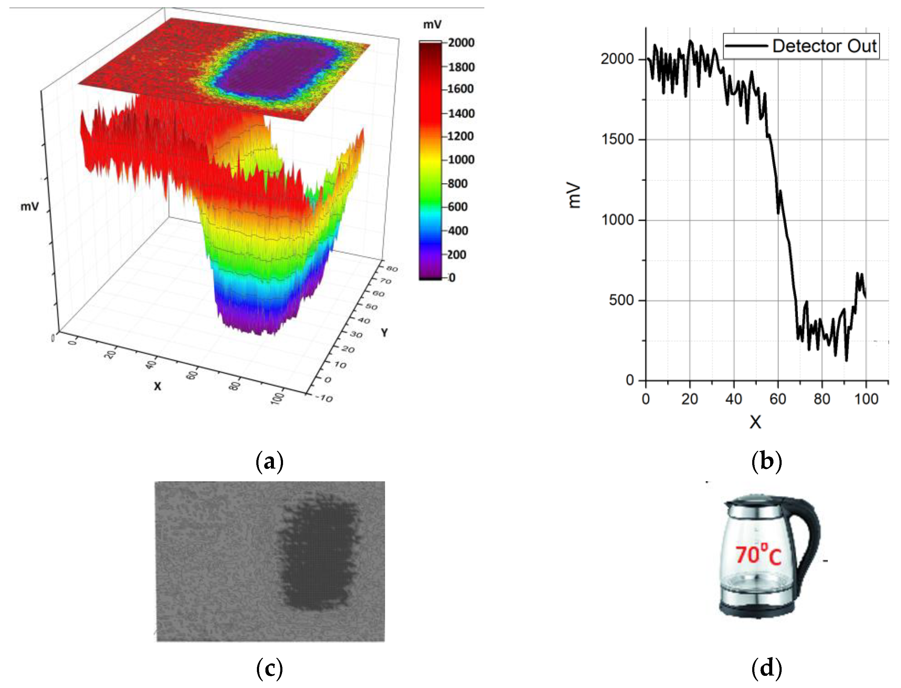
The data collected during the scan were recorded as a matrix when the scan was finished. The recorded data were plotted in OriginLab software [33] and are given in Figure 23. The figure gives both the image and the screen data for scanning a line in the x-axis. A hot sample was displayed in the range of 45 × 80 points on the image. Since the number of steps is 1 mm, it corresponds to a scanning area of 45 mm × 80 mm. This corresponds to approximately 1/3 of the actual dimensions.
4. Conclusions
A low-cost and compact LNRS for passive millimeter-wave imagers capable of remote viewing indoors and outdoors was constructed in this study. In addition, single-pixel PMMWI was performed to determine the properties of the LNRS and acquire images with it. The LNRS has a compact structure due to its dimensions of 20 mm × 20 mm × 85 mm, and thanks to this structure, the array can be made. The millimeter circuit part consists of only an LNA and a detector. It contains the supply circuits required for the LNA and the circuits necessary for detecting the detector output by any ADC. Thus, it does not require complex electronic circuits for its use. As seen in the LNRS measurements, the thermal resolution was calculated as 0.2 K, which was realized as approximately 0.24 K. The PMMWI system has a 240 mm diameter lens and a 300 mm × 300 mm scanner with an accuracy of 0.1 mm.
As a result, LNRS has a structure that can come to the fore in many practical applications and experimental studies due to its compact structure, high resolution, and ease of use.
In future studies, an array will be created with an LNRS, and the quasi-optical imaging system will be converted to a snapshot structure. Thus, a millimeter-wave camera will be obtained.
Author Contributions
M.T., Conceptualization, data curation, formal analysis methodology, and writing—original draft preparation, G.Ç.; methodology, writing—review and editing. All authors have read and agreed to the published version of the manuscript.
Funding
This research received no external funding.
Data Availability Statement
Not applicable.
Conflicts of Interest
The authors declare no conflict of interest.
References
- Siegel, P. Terahertz technology. IEEE Trans. Microw. Theory Technol. 2002, 50, 910–928. [Google Scholar] [CrossRef]
- Yujiri, L.; Shoucri, M.; Moffa, P. Passive millimeter wave imaging. IEEE Microw. Mag. 2003, 4, 39–50. [Google Scholar] [CrossRef]
- Chen, Q.; Fan, Y.; Zhou, J.; Song, K. Design of Quasi-Optical Lens Antenna for W-Band Short Range Passive Millimeter-Wave Imaging. J. Comput. Commun. 2015, 3, 3. [Google Scholar] [CrossRef]
- Kemp, M.C. Millimetre wave and terahertz technology for the detection of concealed threats: A review. Opt. Pho-Tonics Count. Crime Fight. II 2006, 6402, 64020D. [Google Scholar] [CrossRef]
- Olsen, R.; Lovberg, J.A.; Chou, R.-C.; Martin, C.A.; Galliano, J.A., Jr. Passive millimeter-wave imaging using a sparse phased-array antenna. Passiv. Millim.-Wave Imaging Technol. 1997, 3064, 63–70. [Google Scholar] [CrossRef]
- Pergande, A.; Eden, D.D.; McKinley, M.C.; Sutha, S.; Weatherwax, E. Concealed weapons detection sensor and signal-processing demonstration. Passiv. Millim.-Wave Imaging Technol. 1997, 3064, 46–53. [Google Scholar] [CrossRef]
- Pergande, A.N. History and challenges of passive millimeter wave imaging. Millimetre Wave Terahertz Sens. Technol. VI 2013, 8900, 6. [Google Scholar] [CrossRef]
- Li, R.; Li, C.; Li, H.; Wu, S.; Fang, G. Study of Automatic Detection of Concealed Targets in Passive Terahertz Images for Intelligent Security Screening. IEEE Trans. Terahertz Sci. Technol. 2018, 9, 165–176. [Google Scholar] [CrossRef]
- Garcia-Rial, F.; Montesano, D.; Gomez, I.; Callejero, C.; Bazus, F.; Grajal, J. Combining Commercially Available Active and Passive Sensors into a Millimeter-Wave Imager for Concealed Weapon Detection. IEEE Trans. Microw. Theory Technol. 2018, 67, 1167–1183. [Google Scholar] [CrossRef]
- Yao, X.; Liu, K.; Hu, A.; Miao, J. Improved design of a passive millimeter-wave synthetic aperture interferometric imager for indoor applications. Millim. Wave Terahertz Sens. Technol. 2015, 9651, 965105. [Google Scholar] [CrossRef]
- Korolyov, S.; Goryunov, A.; Illarionov, I.; Parshin, V.; Zemlyanukha, P. Millimeter-Wave Imaging System Based on Direct-Conversion Focal-Plane Array Receiver. Sensors 2022, 22, 7132. [Google Scholar] [CrossRef]
- Gong, J.; Chen, X.; He, W.; Altaf, A.; Hu, A.; Miao, J. A V-Band Integrated Receiver Front-End Based on 0.15 μm GaAs pHEMT Process for Passive Millimeter-Wave Imaging. IEEE Access 2022, 10, 59933–59941. [Google Scholar] [CrossRef]
- Guo, L.; Qin, S. High-Performance Detection of Concealed Forbidden Objects on Human Body with Deep Neural Networks Based on Passive Millimeter Wave and Visible Imagery. J. Infrared Millim. Terahertz Waves 2019, 40, 314–347. [Google Scholar] [CrossRef]
- Luomahaara, J.; Sipola, H.; Gronberg, L.; Mayra, A.; Aikio, M.; Timofeev, A.; Tappura, K.; Rautiainen, A.; Tamminen, A.; Vesterinen, V.; et al. A Passive, Fully Staring THz Video Camera Based on Kinetic Inductance Bolometer Arrays. IEEE Trans. Terahertz Sci. Technol. 2020, 11, 101–108. [Google Scholar] [CrossRef]
- Beig, M.T.A.; Kumar, M.; Sharma, Y.; Sharma, B.K. A Terahertz/Millimeter-Wave Based Detection and Imaging System Using Antenna-Coupled Microbolometer. J. Phys. Conf. Ser. 2022, 2335, 12005. [Google Scholar] [CrossRef]
- Wang, J.; Naftaly, M.; Wasige, E. An Overview of Terahertz Imaging with Resonant Tunneling Diodes. Appl. Sci. 2022, 12, 3822. [Google Scholar] [CrossRef]
- Zhang, Y.; Zhang, S. Novel CMOS-based multi-band terahertz detector for passive imaging. Semicond. Sci. Technol. 2022, 37, 055014. [Google Scholar] [CrossRef]
- Planck, M. Zur Theorie des Gesetzes der Energieverteilung im Normalspektrum (On the Theory of the Energy Distribution Law of the Normal Spectrum. Verh. Der Dtsch. Phys. Gesselschaft 1900, 2, 237. [Google Scholar]
- Meng, Y.; Qing, A.; Lin, C.; Zang, J.; Zhao, Y.; Zhang, C. Passive Millimeter Wave Imaging System Based on Helical Scanning. Sci. Rep. 2018, 8, 7852. [Google Scholar] [CrossRef]
- Sinclair, G.N.; Appleby, R.; Coward, P.R.; Price, S. Passive millimeter-wave imaging in security scanning. Passiv. Millim.-Wave Imaging Technol. 2000, 4032, 40–45. [Google Scholar] [CrossRef]
- Vine, D.L.; Skou, N. Microwave Radiometer Systems: Design and Analysis, 2nd ed.; Artech: Norwood, MA, USA, 2006; p. 1. Available online: https://ieeexplore-ieee-org.uml.idm.oclc.org/document/9101160 (accessed on 8 December 2022).
- Available online: https://www.ommic.com/datasheets/OMMIC_DATASHEET_LNA_CGY2190UH-C2.pdf (accessed on 1 December 2022).
- Available online: https://www.ommic.com/datasheets/OMMIC_DATASHEET_ZBD_CGY2870AUH-C1.pdf (accessed on 1 December 2022).
- RT/Duroid® 5880 Laminates—Rogers Corporation. Available online: https://www.rogerscorp.com/advanced-electronics-solutions/rt-duroid-laminates/rt-duroid-5880-laminates (accessed on 11 December 2022).
- Appleby, R. The history of passive millimetre-wave imaging at QinetiQ. Millimetre Wave Terahertz Sens. Technol. 2008, 7117, 2. [Google Scholar] [CrossRef]
- Vertiy, A.; Tekbas, M.; Kizilhan, A.; Panin, S.; Ozbek, S. Sub-Terahertz Radiometric Imaging System for Concealed Weapon Detection. Available online: https://scholar.google.com/scholar?hl=en&as_sdt=0%2C5&q=Sub-terahertz+radiometric+imaging+system+for+concealed+weapon+detection%3BAlexey+Vertiy%2C+Mustafa+Tekbas%2C+Ahmet+Kizilhan%2C+Sergey+Panin%2C+Sunullah+OzbekPIERS-2010%2C+Cambridge%2C+US&btnG= (accessed on 11 December 2022).
- Vertiy, A.; Ozbek, S.; Pavlyuchenko, A.; Tekbas, M.; Kizilhan, A.; Cetinkaya, H.; Unal, A.; Panin, S. Passive radiometric imaging systems in millimeter wavelength range. In Proceedings of the 2011 IEEE International Symposium on Antennas and Propagation (APSURSI), Spokane, WA, USA, 3–8 July 2011; pp. 2111–2114. [Google Scholar] [CrossRef]
- Huguenin, G.R. Millimeter-wave concealed weapons detection and through-the-wall imaging systems. Command. Control. Commun. Intell. Syst. Law Enforc. 1997, 2938, 152–159. [Google Scholar] [CrossRef]
- Fetterman, M.R.; Grata, J.; Jubic, G.; Kiser, J.W.L.; Visnansky, A. Simulation, acquisition and analysis of passive millimeter-wave images in remote sensing applications. Opt. Express 2008, 16, 20503–20515. [Google Scholar] [CrossRef] [PubMed]
- Zhang, J.; Zhu, W.; Zhao, Y.; Zhao, R.; Dong, L. Passive THz Imaging System Based on the Crank-Rocker Mechanism. Acta Opt. Sin. 2013, 33, 1211006. [Google Scholar] [CrossRef]
- Oliver, G. Low-Loss Materials in High Frequency Electronics and the Challenges of Measurement. Available online: https://wiki.epfl.ch/thz/documents/Materials%20and%20Measurements%20-%20DuPont%20-%20Feb2015.pdf (accessed on 20 May 2023).
- Lo, Y.T.; Lee, S.W. Antenna Handbook, 1st ed.; (Ch. 16. Lee, J.J. Lens Antennas); Springer: New York, NY, USA, 1988; pp. 1073–1131. [Google Scholar] [CrossRef]
- OriginLab—Origin and OriginPro—Data Analysis and Graphing Software. Available online: https://www.originlab.com/ (accessed on 9 September 2022).
Figure 1.
Optic camera.
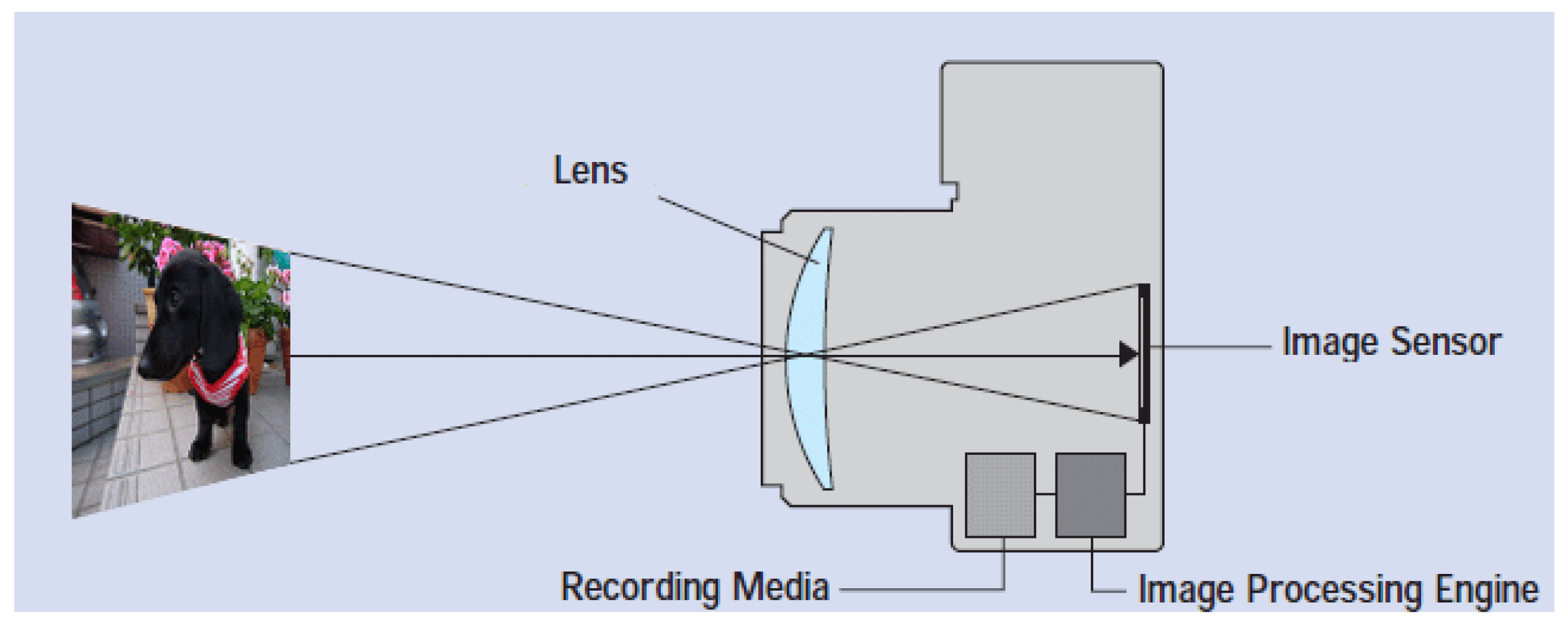
Figure 2.
PMMWI diagram.
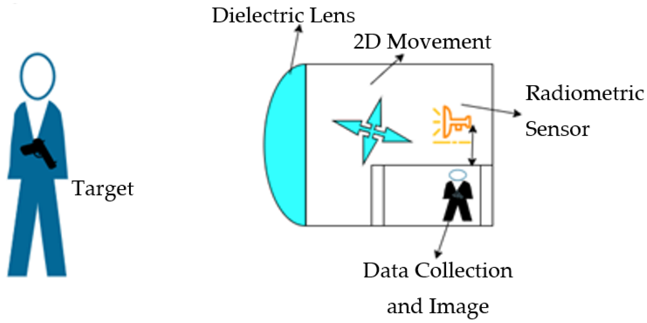
Figure 3.
Ideal LNRS.
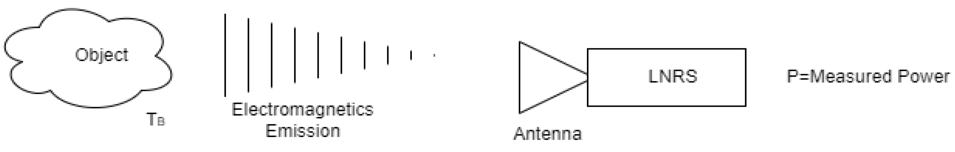
Figure 4.
Real receiver structure [21].
Figure 4.
Real receiver structure [21].
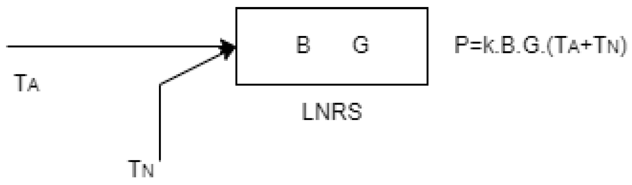
Figure 5.
Resolution analysis (a) B = 10 GHz; NF vs. τ; (b) τ = 1 ms; B vs. NF.
Figure 6.
LNRS block structure.
Figure 7.
WR-10 waveguide MS line transition: (a) position and (b) line sizes.

Figure 8.
WR-10 Waveguide MS line transition simulation result.
Figure 9.
LNRS Connections.
Figure 10.
LNRS photographs: (a) outside and (b) inside.
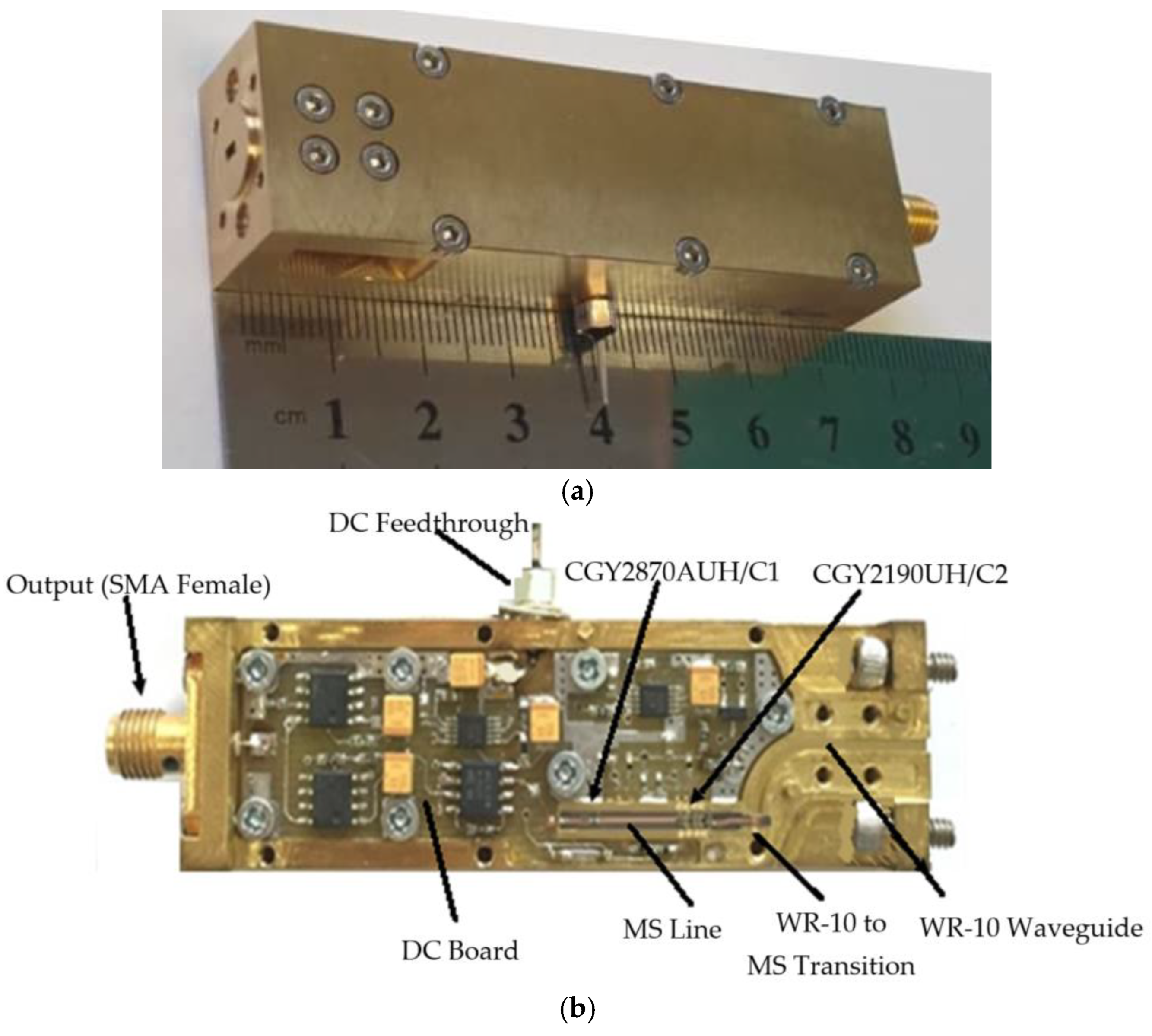
Figure 11.
Quasi Optical Imaging System with Dielectric Lens.
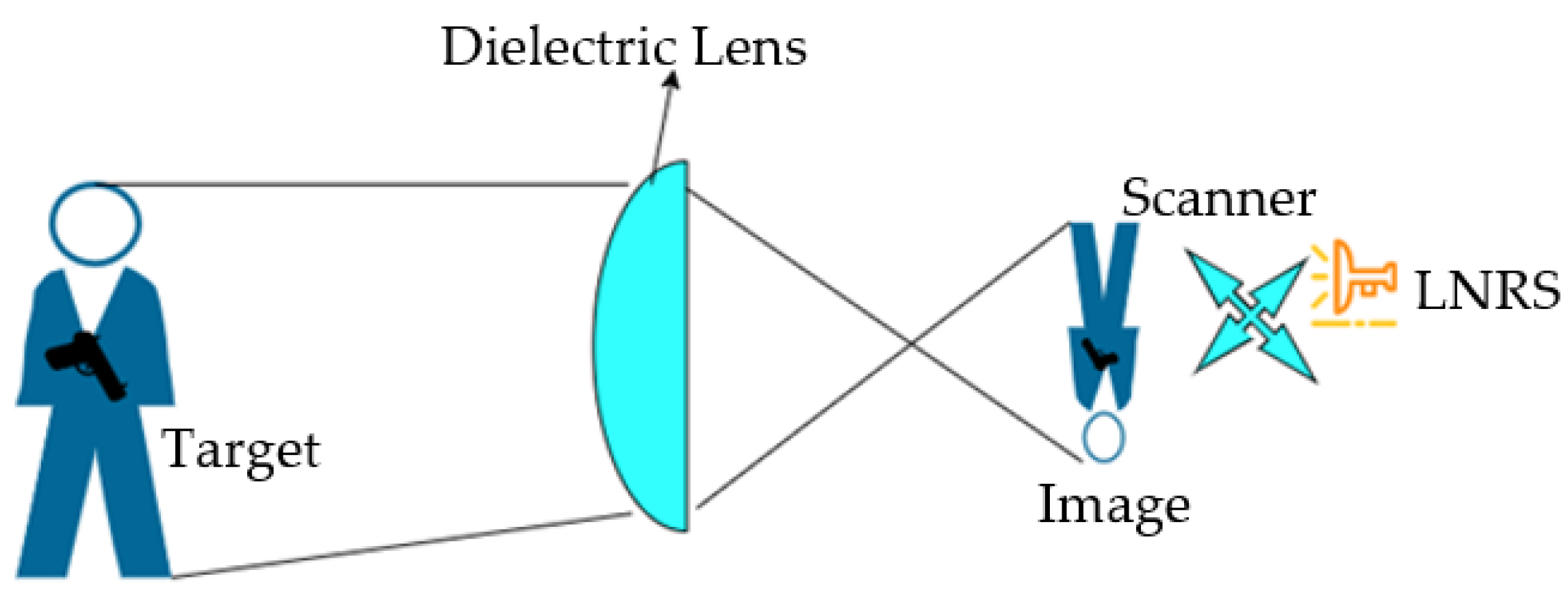
Figure 12.
Quasi-optical imaging system using a reflector.
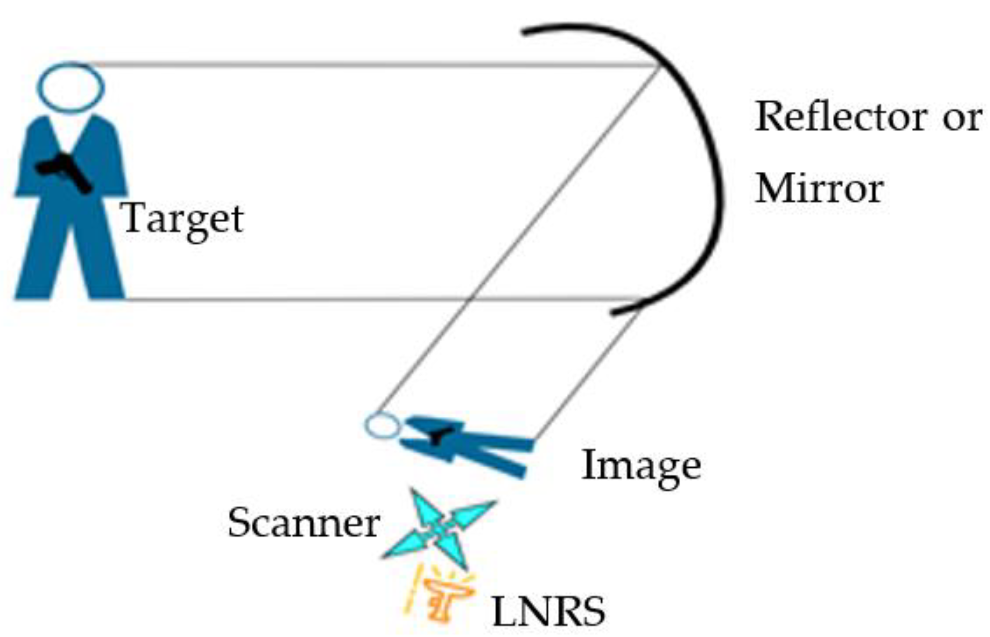
Figure 13.
Display scenario.
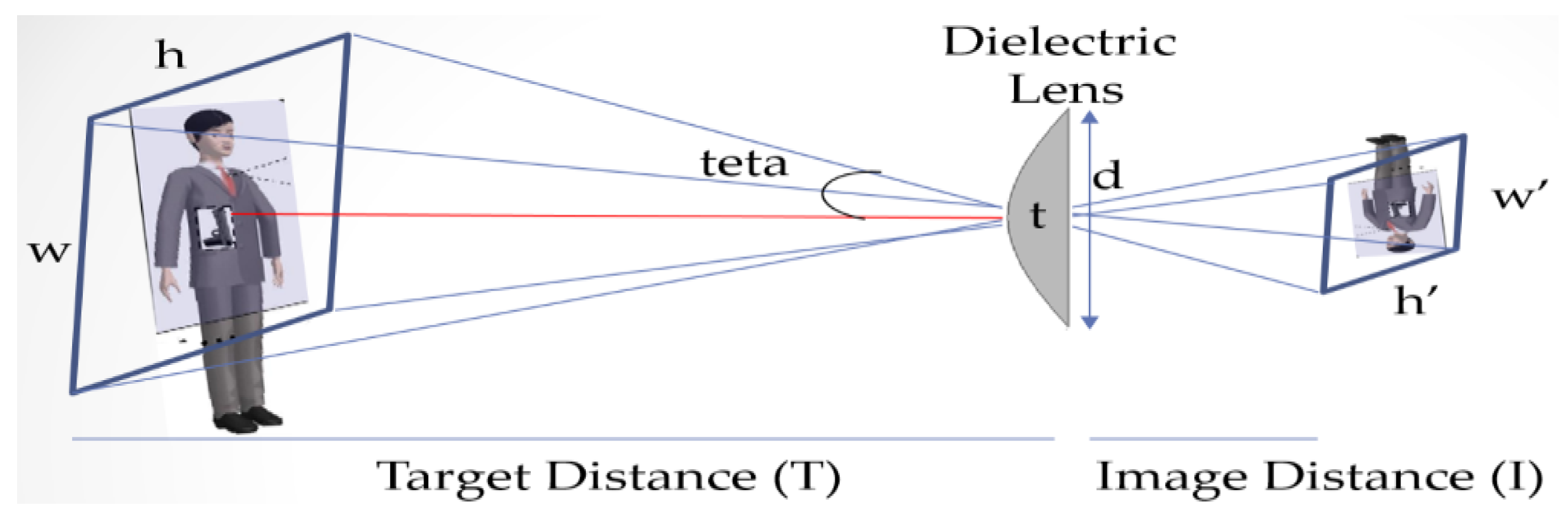
Figure 14.
Lens Geometry.
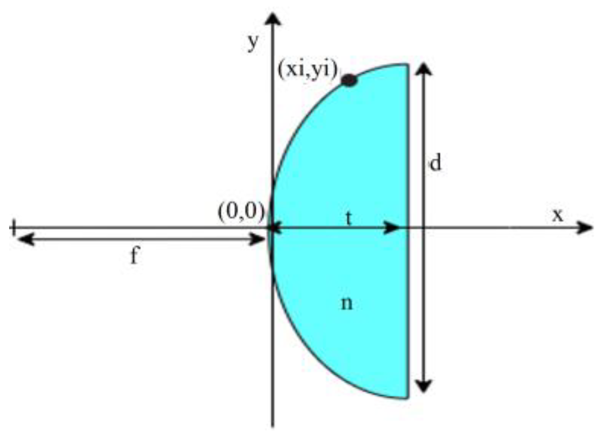
Figure 15.
Teflon dielectric lens: (a) pre-production technical drawing and (b) the produced lens.
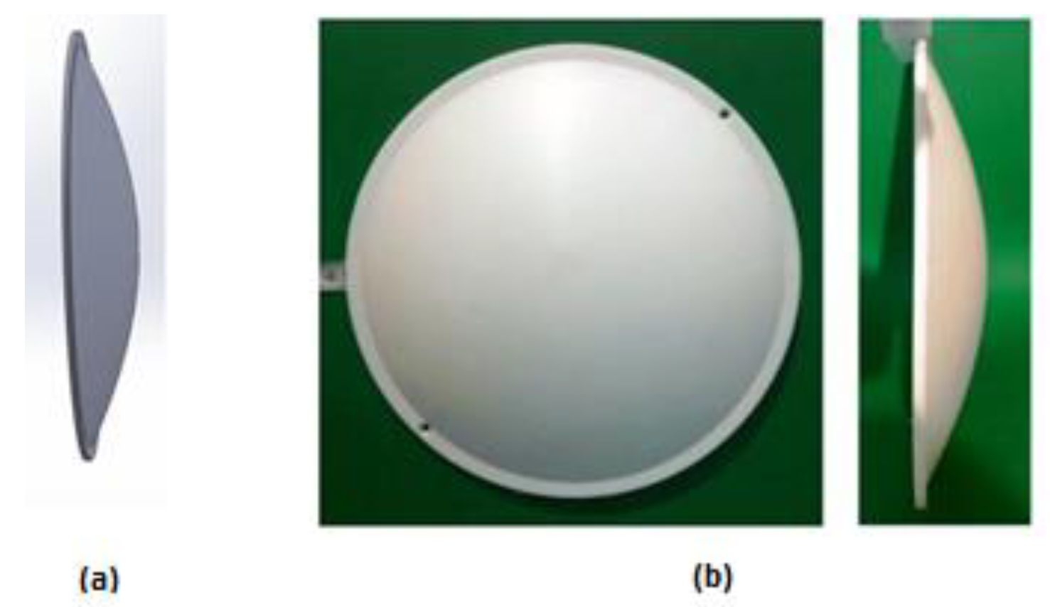
Figure 16.
Cartesian scanner.
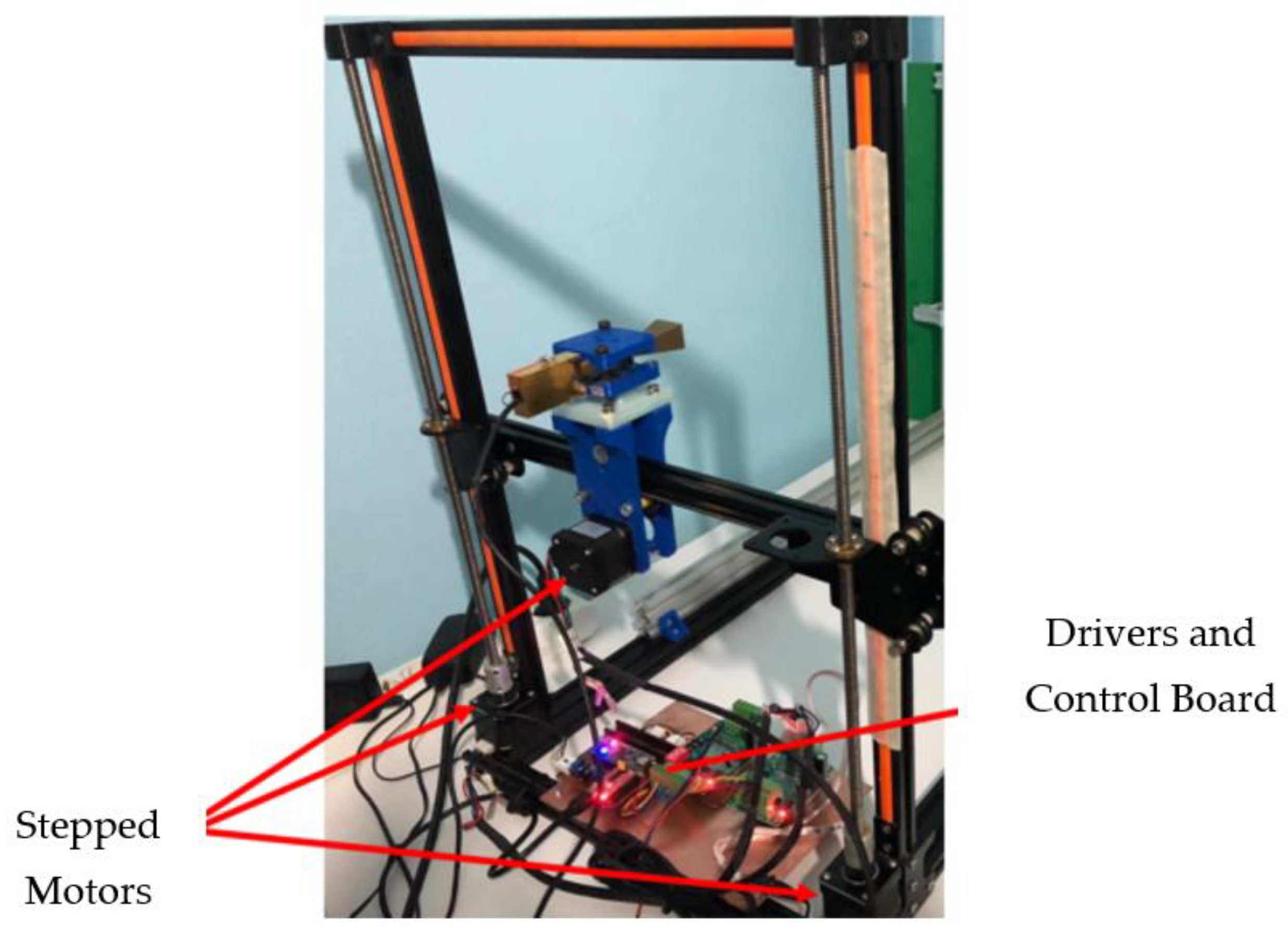
Figure 17.
Quasi-optical imaging system.
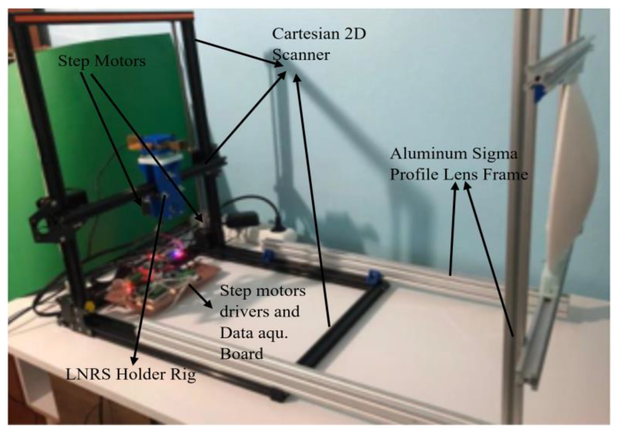
Figure 18.
The scanning and data collection topology.
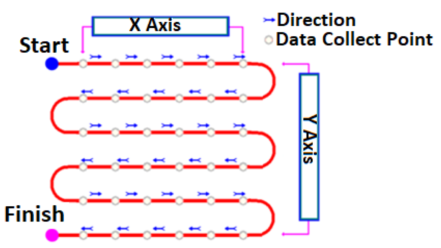
Figure 19.
PWMMI measurement scenario.
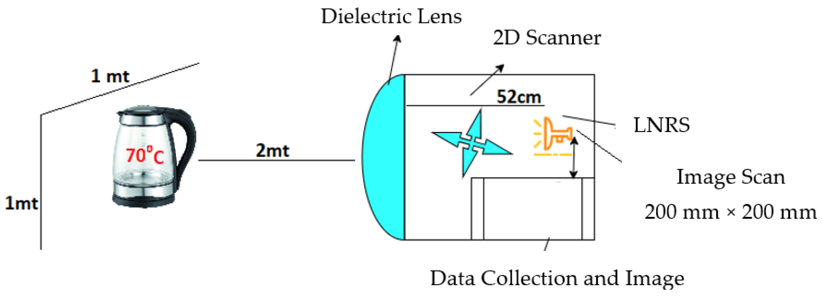
Figure 20.
LNRS distance measurement result.
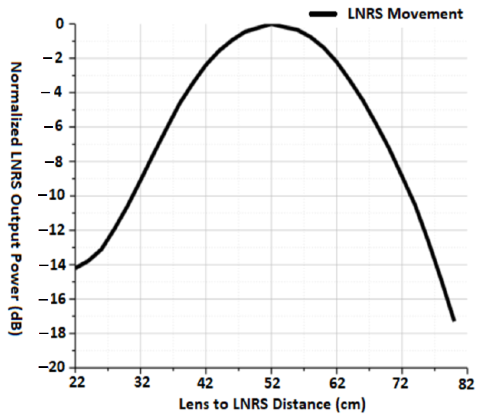
Figure 21.
PMMWI (a) measuring setup and (b) software interface.
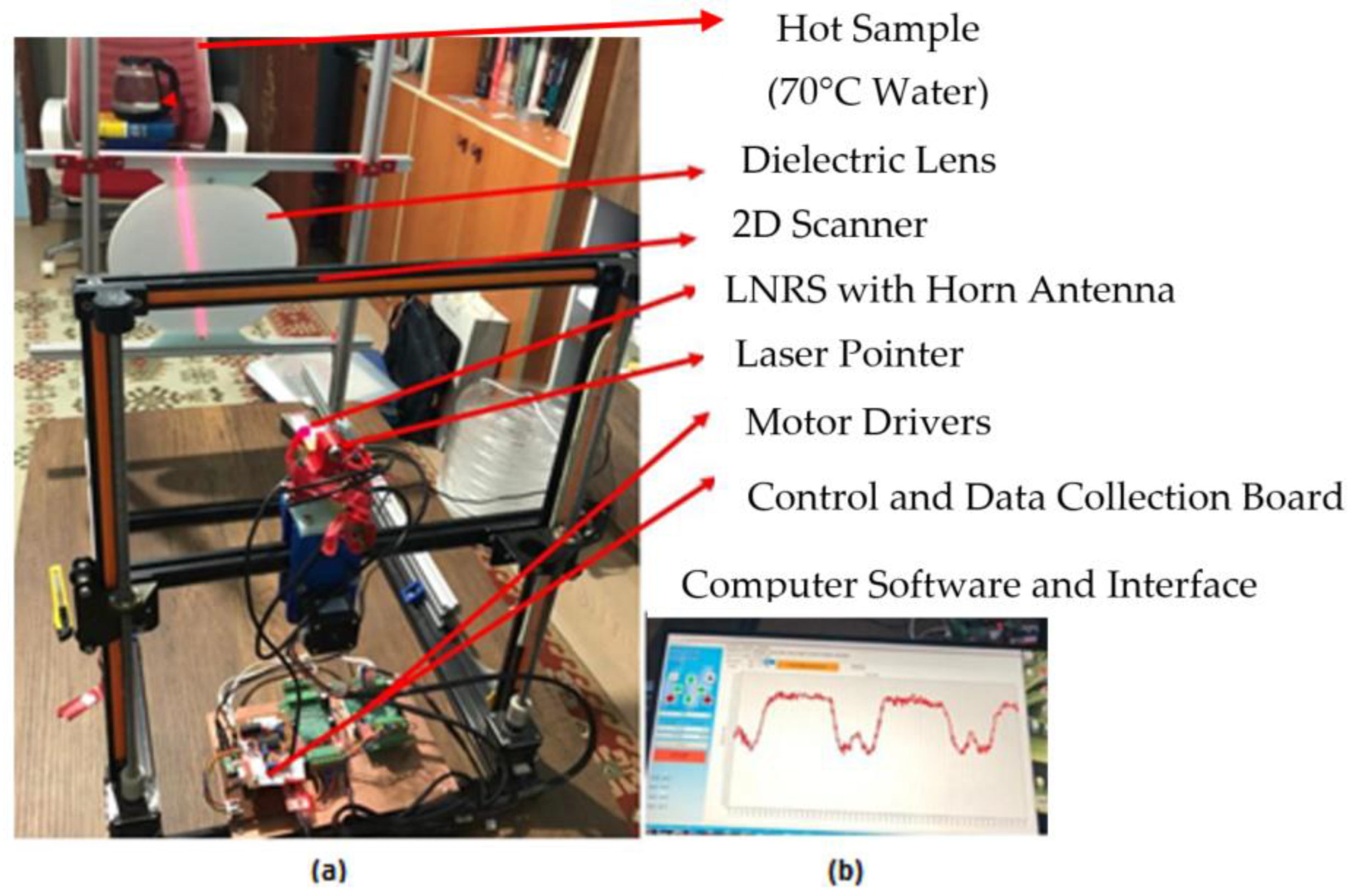
Figure 22.
Measurement screen scan results.
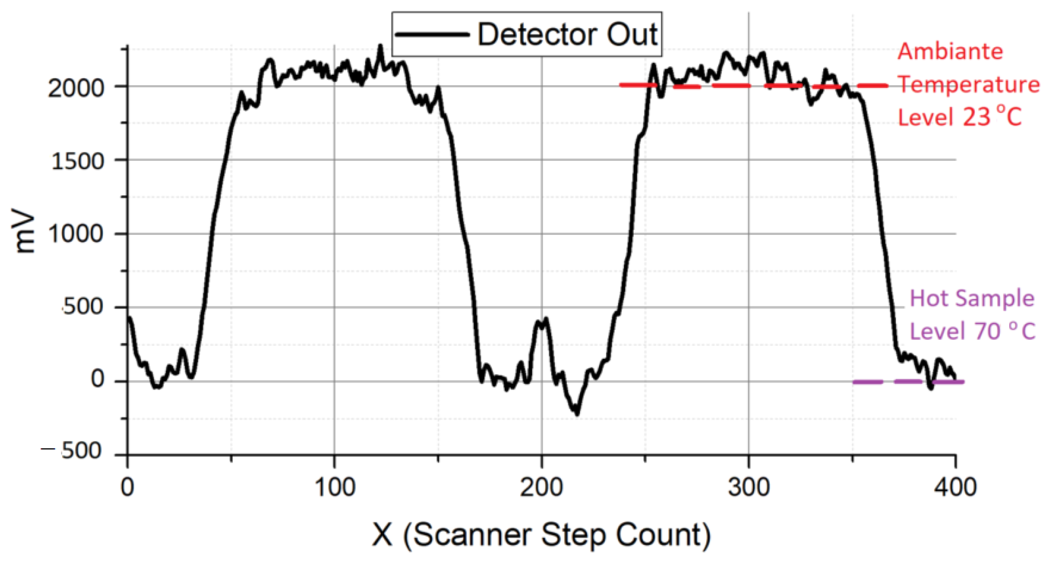
Figure 23.
PMMWI image: (a) 3D/2D image; (b) one line (Y = 40) of data (LNRS output) along the x-axis; (c) 2D grey scale image; and (d) target.
Figure 23.
PMMWI image: (a) 3D/2D image; (b) one line (Y = 40) of data (LNRS output) along the x-axis; (c) 2D grey scale image; and (d) target.

Table 1.
LNRS structures and specifications.
| Technology | Resolution | Cost | Circuit Diagram | Max. Freq. |
|---|---|---|---|---|
| Direct Detection | Acceptable | Low |  | 0.6 THz |
| Direct Detection with LNA | Good | Low |  | 0.3 THz |
| Heterodyne | Good | High | 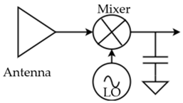 | 1 THz |
| Micro Bolometer | Poor | Low | 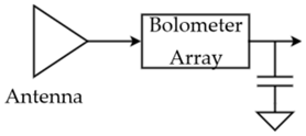 | 1 THz |
Disclaimer/Publisher’s Note: The statements, opinions and data contained in all publications are solely those of the individual author(s) and contributor(s) and not of MDPI and/or the editor(s). MDPI and/or the editor(s) disclaim responsibility for any injury to people or property resulting from any ideas, methods, instructions or products referred to in the content. |
© 2023 by the authors. Licensee MDPI, Basel, Switzerland. This article is an open access article distributed under the terms and conditions of the Creative Commons Attribution (CC BY) license (https://creativecommons.org/licenses/by/4.0/).
Share and Cite
MDPI and ACS Style
Tekbaş, M.; Çakır, G. A Compact W-Band Low-Noise Radiometry Sensor for a Single-Pixel Passive Millimeter-Wave Imager. Electronics 2023, 12, 2330. https://doi.org/10.3390/electronics12102330
AMA Style
Tekbaş M, Çakır G. A Compact W-Band Low-Noise Radiometry Sensor for a Single-Pixel Passive Millimeter-Wave Imager. Electronics. 2023; 12(10):2330. https://doi.org/10.3390/electronics12102330
Chicago/Turabian StyleTekbaş, Mustafa, and Gonca Çakır. 2023. "A Compact W-Band Low-Noise Radiometry Sensor for a Single-Pixel Passive Millimeter-Wave Imager" Electronics 12, no. 10: 2330. https://doi.org/10.3390/electronics12102330
Note that from the first issue of 2016, this journal uses article numbers instead of page numbers. See further details here.