Article

Experimental Comparison of a New 1.2 kV 4H-SiC Split-Gate MOSFET with Conventional SiC MOSFETs in Terms of Reliability Robustness

National ASIC System Engineering Research Center, School of Electronic Science and Engineering, Southeast University, Nanjing 211189, China
*
Author to whom correspondence should be addressed.
Electronics 2023, 12(11), 2551; https://doi.org/10.3390/electronics12112551
Submission received: 30 April 2023 / Revised: 24 May 2023 / Accepted: 1 June 2023 / Published: 5 June 2023

Abstract

:
In this paper, we compare a new 1.2 kV rated 4H-SiC split-gate (SG) MOSFET with the conventional planar-gate (PG) MOSFETs. Both structures were fabricated with the same design rules and process platform. Therefore, the structures have similar electrical parameters, such as ON-state drain-source resistance (RON), breakdown voltage (BV), threshold voltage (Vth), and body diode forward voltage (VSD). It is shown that the Ciss/Coss/Crss capacitances of the SG-MOSFET can be reduced by 7%/8%/17%, respectively, compared with PG-MOSFET. It is also shown that the SG-MOSFET has the potential to reduce switching losses without compromising the static performance. Moreover, it maintains the robustness of the device, and an optimized layout design with spaced holes in the gate poly is adopted. Therefore, there is no obvious degradation between the SG-MOSFET and the PG-MOSFET in terms of avalanche and short-circuit endurance capabilities.

1. Introduction

Silicon carbide power MOSFETs are promising for high-speed and high-power applications due to their fast switching capability and low conduction power losses [1,2]. To improve the switching power loss of devices, the gate-drain capacitance (CGD) needs to be reduced during the charging and discharging of it, which can be effectively suppressed by the split-gate structure. However, split-gate MOSFETs (SG-MOSFETs) have critical problems with the gate oxide for the critical electric field appearing at the split-gate oxide corner, which may cause device failure or oxide degradation [3]. In addition to the above effects, in the split-gate structure, the specific resistance of the junction field effect transistor (JFET) region increases as the gate length decreases [1,3,4]. A novel method has been used to suppress the electric field intensity under gate oxide for the split-gate SiC MOSFETs [5,6]. However, in most articles on split gate devices, only design-level optimization is carried out to reduce the electric field at the split gate, and the dynamic and static characteristics of the device compared to traditional devices reflect the advantages of split gate devices. Analysis of device robustness is rarely seen [4,5,6,7].
In this work, the SiC SG-MOSFET was designed and manufactured with a discontinuous digging structure. Gate removal must have no other detrimental effects on device performance to maintain low conduction losses and blocking capabilities [8,9,10,11,12,13]. Both specific ON-resistance (RON,sp) and the BV of the device should be comparable to the PG-MOSFET with a similar voltage rating. Due to the discontinuous digging structure of the SG-MOSFET, both the reverse-transfer capacitance (Crss) and the gate charge (Qg) are reduced for the reduction in the gate-to-drain overlap. Moreover, the reliability failure mechanism of SG-MOSFETs is revealed by the results of the 2D simulation by Silvaco TCAD.

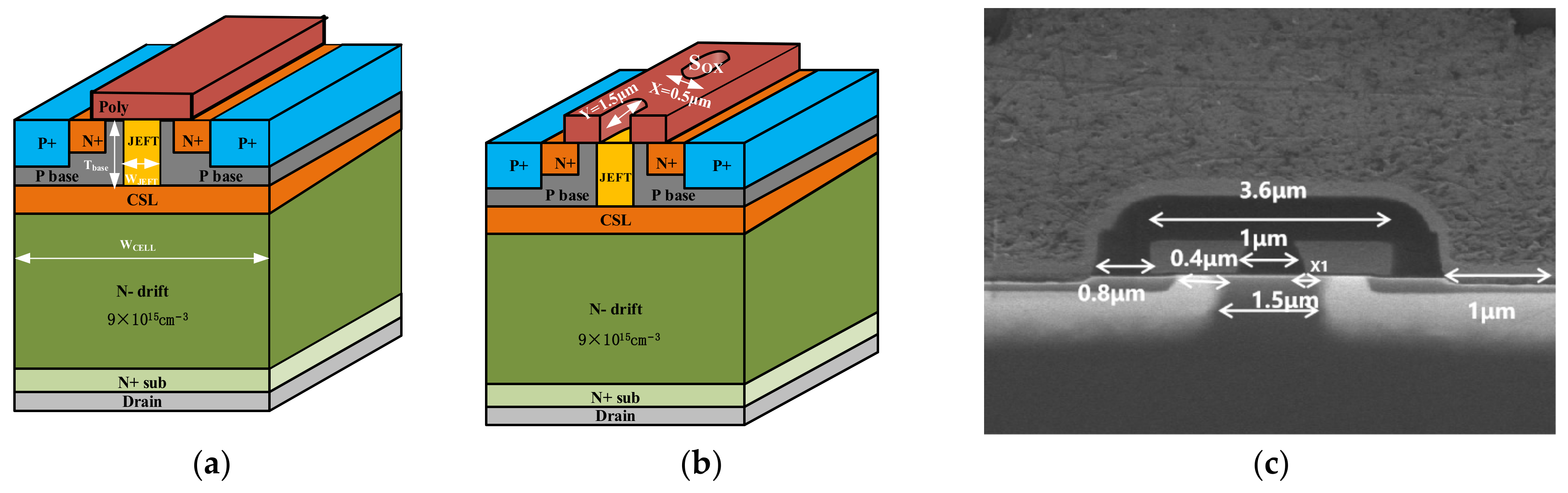
2. Device Design and Fabrication

In this work, the 1.2 kV 4H-SiC power MOSFET has been investigated and fabricated on a 4H-SiC substrate with a 4° inclination angle. The silicon carbide epitaxial layer has a doping concentration of 9 × 1015 cm−3 and a thickness of 10 μm. Both the SG-MOSFET and the PG-MOSFET were fabricated with the same linear cell topology, whose cell pitch is 8.2 μm. This is a self-aligned source/base process to form the MOS channel. It has been previously shown that 1200 V SiC power MOSFETs with a channel length of 0.4 µm can be manufactured with a good yield for the case of a gate oxide thickness of 50 nm [14]. The doping concentration for the N-type JFET region is enhanced to 1 × 1017 cm−3 with nitrogen ion implantation. A JFET width of 1.8 µm is adopted for the linear cell topology. Once the ion implantation is completed, an activation anneal of 1700 °C for 10 min is applied, followed by the gate oxidation process. A 50 nm thick gate oxide is formed by an 1175 °C thermal oxidation in N2O ambient, followed by the post-oxidation anneal in NO. The gate polysilicon is then deposited and patterned, followed by the deposition of the interlevel dielectric (ILD), which is subsequently patterned and etched for the front side ohmic contacts. Nickel is then deposited for the ohmic contact on the front side and underwent a silicitation process, after which the unsilicited nickel is removed from the front side. The backside nickel is then deposited, and both back and front ohmic contacts undergo an ohmic anneal of approximately 900 °C for 5 min. Following the anneal, a thick layer of aluminum is deposited and patterned for both the gate and the source pads. The front sides of the PG-MOSFET and the SG-MOSFET are then passivated using nitride and polyimide [1]. Their 3D cross-sectional schematic views and the SEM (scanning electron microscope) photo of the SG-MOSFET are shown in Figure 1. The design parameters for SG-MOSFET and PG-MOSFET are shown in Table 1.

3. Electrical Characteristics and Discussion

3.1. Static Electrical Characteristics

The typical electric characteristics of the fabricated PG-MOSFET and SG-MOSFET are shown in Figure 2. Their BV is nearly 1600 V, as shown in Figure 2a. In Figure 2b, the Vth are both 2.6 V. No difference is shown between the two devices. The Id–Vd characteristics of the two structures in Figure 2c are consistent with each other. The calculated RON,sp of the PG-MOSFET is 5 mΩ∙cm2, while that of the SG-MOSFET is 5.12 mΩ∙cm2. In the third quadrant, the IV curves are measured with the same bias (VGS = −4 V). The VSD are both 4 V at ID = 5 A [15].
As expected, the data above confirm that the implementation of the SG device has no negative influence on the performance when compared with the PG device, as a minimal difference is observed between the reported RON,sp values. Because the slots with continuous circular holes (X = 0.5 μm, Y = 1.5 μm) are etched on the polysilicon gate of this SG structure, Figure 1c shows the structure from a fabricated SG-MOSFET with a reduced JFET width. The device suffers from a pinching effect due to the increased lateral straggle within the P-well, causing a small increase in RON,sp when compared with the PG-MOSFET. Additionally, there is no difference between the transconductance or the gate-source breakdown of the devices with different gate structures.

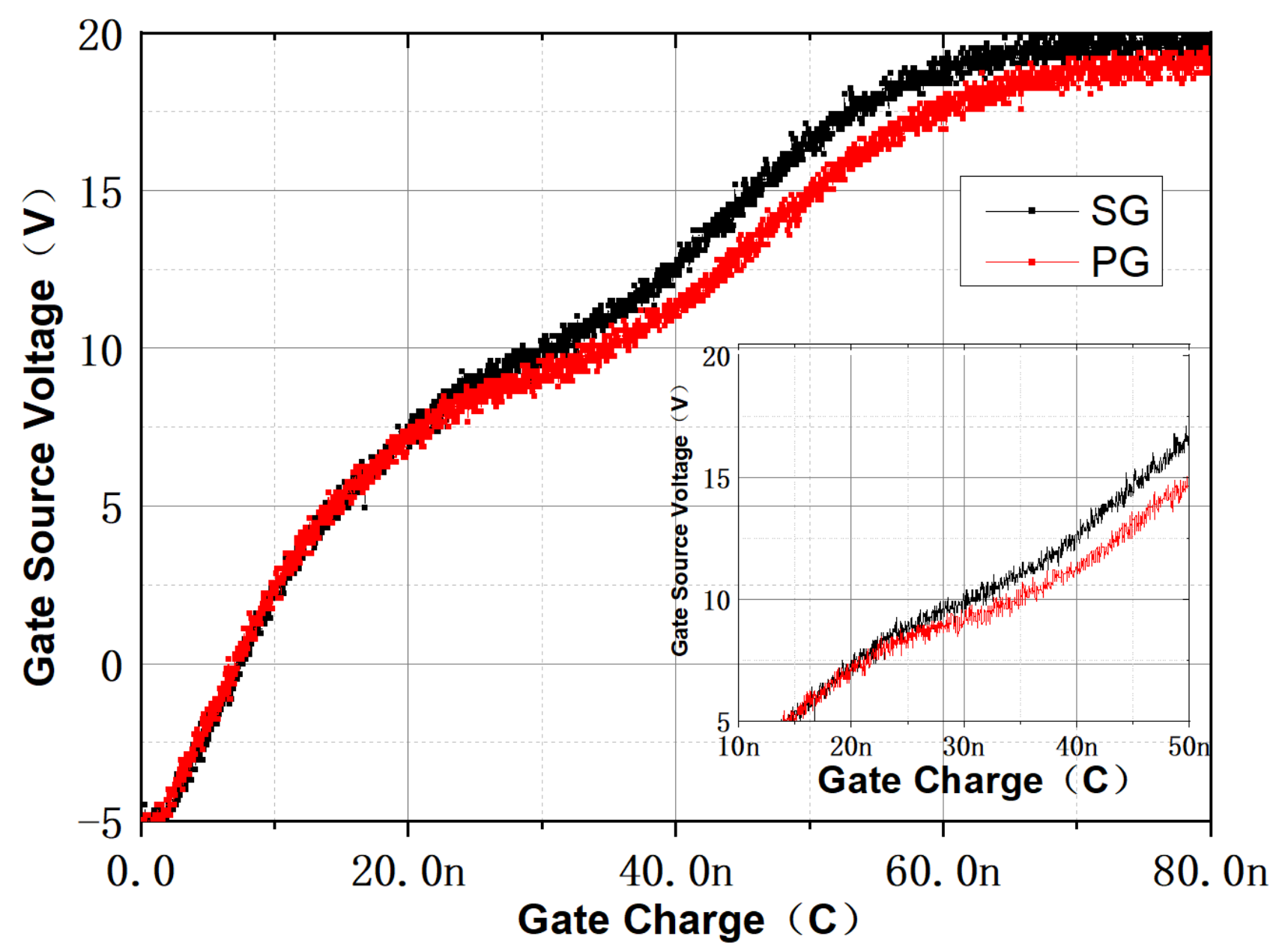
3.2. Dynamic Electrical Characteristics

The main benefit of the SG structure, as discussed in the introduction, is the reduction in the CGD. Figure 3 and Figure 4 show the measured dynamic characteristics of the fabricated SG-MOSFET and PG-MOSFET. The Ciss/Coss/Crss of the SG-MOSFET are lower than those of the PG-MOSFET, as shown in Figure 3. The Ciss of the SG-MOSFET at VDS = 0 V is 2.07 nF, while it is 1.93 nF for the PG one. More significantly, the Crss of the SG-MOSFET at VDS = 0 V is 756 pF, which is about 1.2 times smaller than the 914 pF for the PG-MOSFET. The significant reduction in the CGD can be explained by the geometric factor. The CGD is proportional to (W0-X1)/Wcell, where W0 is the JFET depletion width, Wcell is the half-cell pitch, and X1 is a function of polysilicon gate overhang into the JEFT region, as shown in Figure 1c [4].
The measured gate charge waveforms at VDS = 800 V and ID = 20 A of both the SiC MOSFETs are plotted in Figure 4. The QGD obtained from the gate voltage plateaus is 80 nC for the PG-MOSFET and 72 nC for the SG-MOSFET. The observed reduction by a rate of 10% provides experimental confirmation of the improved switching performance of the 4H-SiC SG-MOSFET. The electrical characteristics of the SG-MOSFET were compared with those of the PG-MOSFET in Table 2.

4. Experimental Results and Discussion

Although the capacitance characteristics of the SG-MOSFET improved, there may be reliability risks. Therefore, we conducted unclamped inductance stress (UIS) and short-circuit (SC) tests to verify the ultimate reliability of this device.

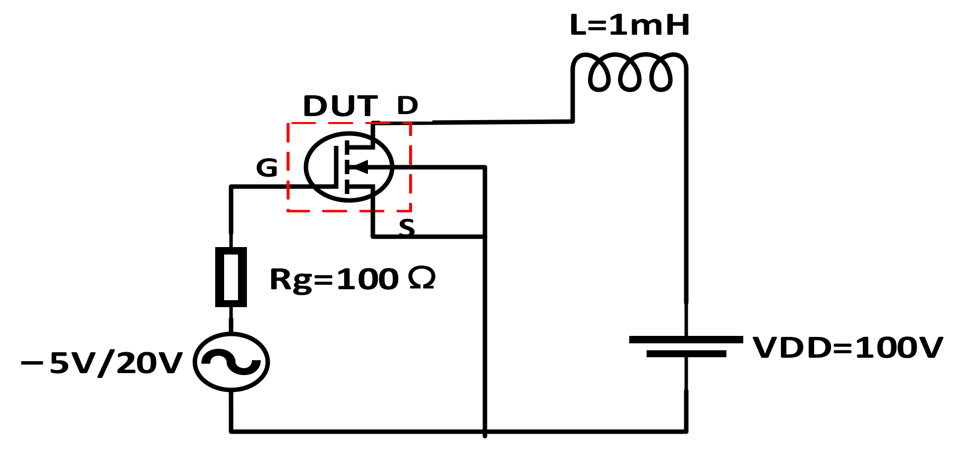
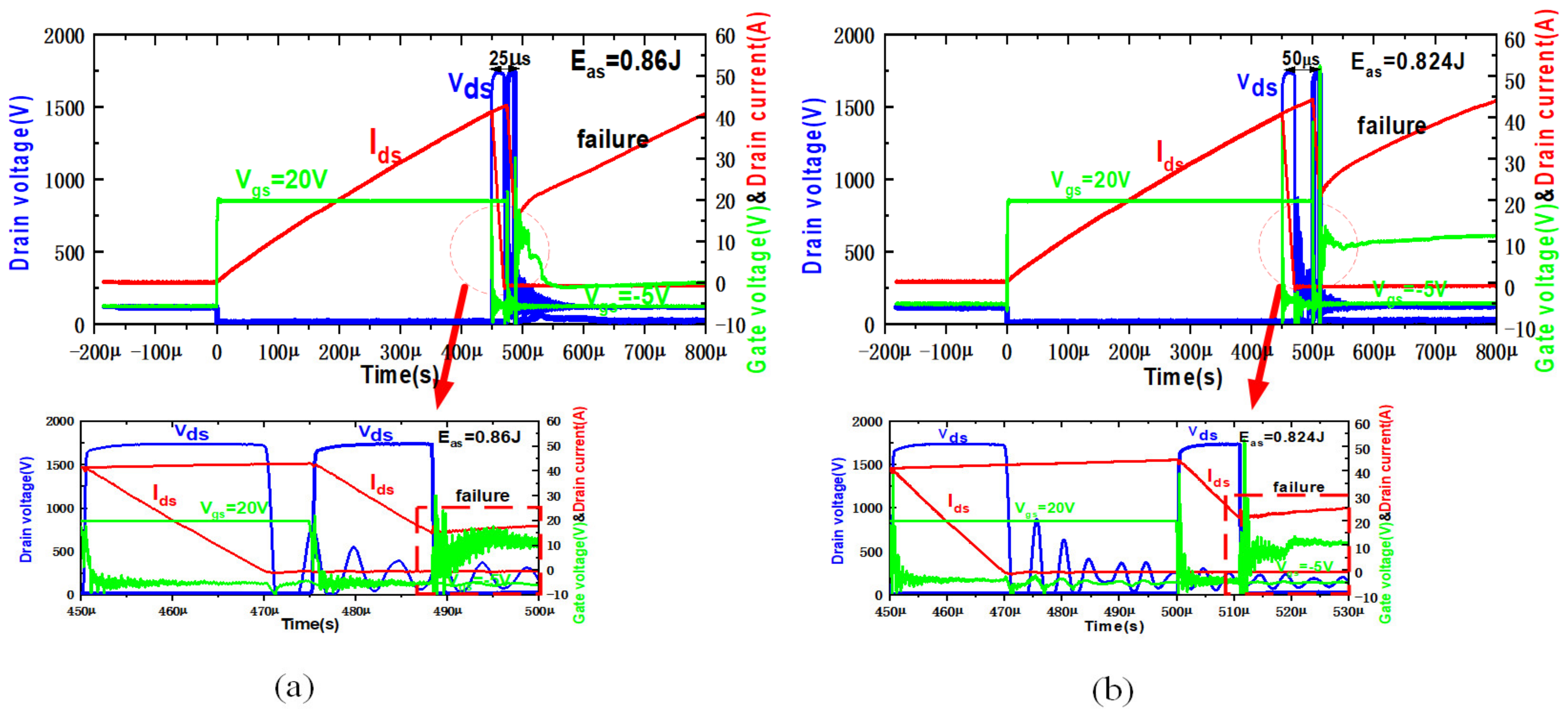
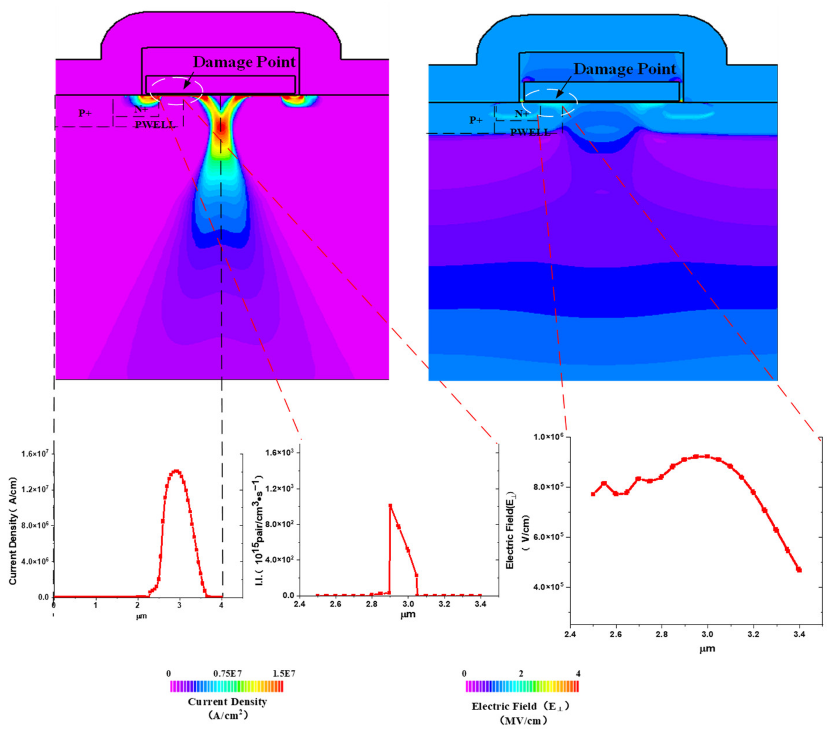
4.1. UIS Characteristics

Figure 5 shows the UIS measurement test circuit for the PG-MOSFET and SG-MOSFET. During the UIS tests, the VDD was 100 V, while the VGS was 20/−5 V [16]. An inductor of 1 mH was used to charge the avalanche energy. A gate resistor of 100 Ω was connected to the gate driver to avoid undesirable voltage surges. Meanwhile, the duration of the charging time ton was increased by 10 μs per UIS pulse until the device failed. The maximum endurable UIS energy density (Eas) is calculated using Formula (1):
E as = 1 2 I A S 2 L B V DSS B V DSS V DD
The measured UIS waveforms of the SG-MOSFET and the PG-MOSFET just before and after failure are plotted in Figure 6. As shown in Figure 6a, when the pulse time reaches 470 μs, the ID is 41.47 A. Then, the gate turns off, resulting in avalanche status. After 25 μs, the I load reaches 0 A, ending the avalanche stress. Abnormal gate voltage waveforms occur when UIS failure happens. Actually, the gate, the drain, and the source are short-circuited to each other for both devices. The Eas of the PG-MOSFET is calculated to be 0.86 J. As shown in Figure 6b, when the pulse time reaches 470 μs, the ID is 40.60 A. From Figure 6b, it can be seen that the device is still normal. After the next 50 μs impact, it is found that the device is broken, meaning the gate voltage curve cannot be turned off normally. The calculated Eas of the SG-MOSFET is 0.824 J. Both SiC MOSFETs can endure a similar Eas, implying that the avalanche capabilities of them are almost the same. Figure 7a,b, respectively, show the post-failure chip surfaces of the SG-MOSFET and PG-MOSFET after delidding. There are obvious burn marks on the bonding footprints. It indicates that both devices die from the instantaneous high temperature.
Since the surfaces of the two devices were burned out after UIS, the Silvaco TCAD was used to simulate the process to explain the lattice temperature and electric field of the devices during the UIS process. It can be reflected from Figure 8 that the temperature of the Al layer of the two devices reached above 700 K during the UIS process [18]. The melting point of the Al layer was reached, thus the devices appear to burn out of the Al layer. According to the simulation, the internal lattice temperature between SG-MOSFET and PG-MOSFET is different only by about 100 K. Meanwhile, the electric field at gate oxide is shown in Figure 9, the SG-MOSFET is at 5.8 MV/cm and the PG-MOSFET is at 4.2 MV/cm, which found that SG-MOSFET has a stronger electric field at the corner under the UIS test.

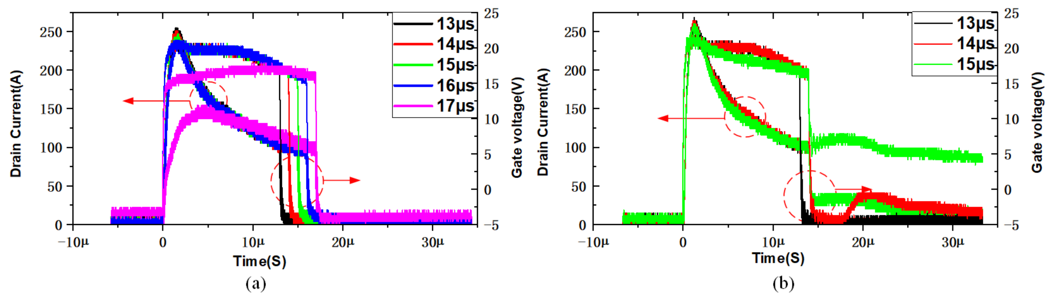
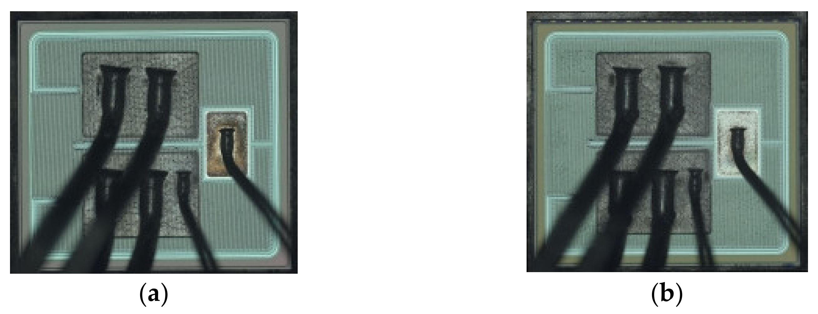
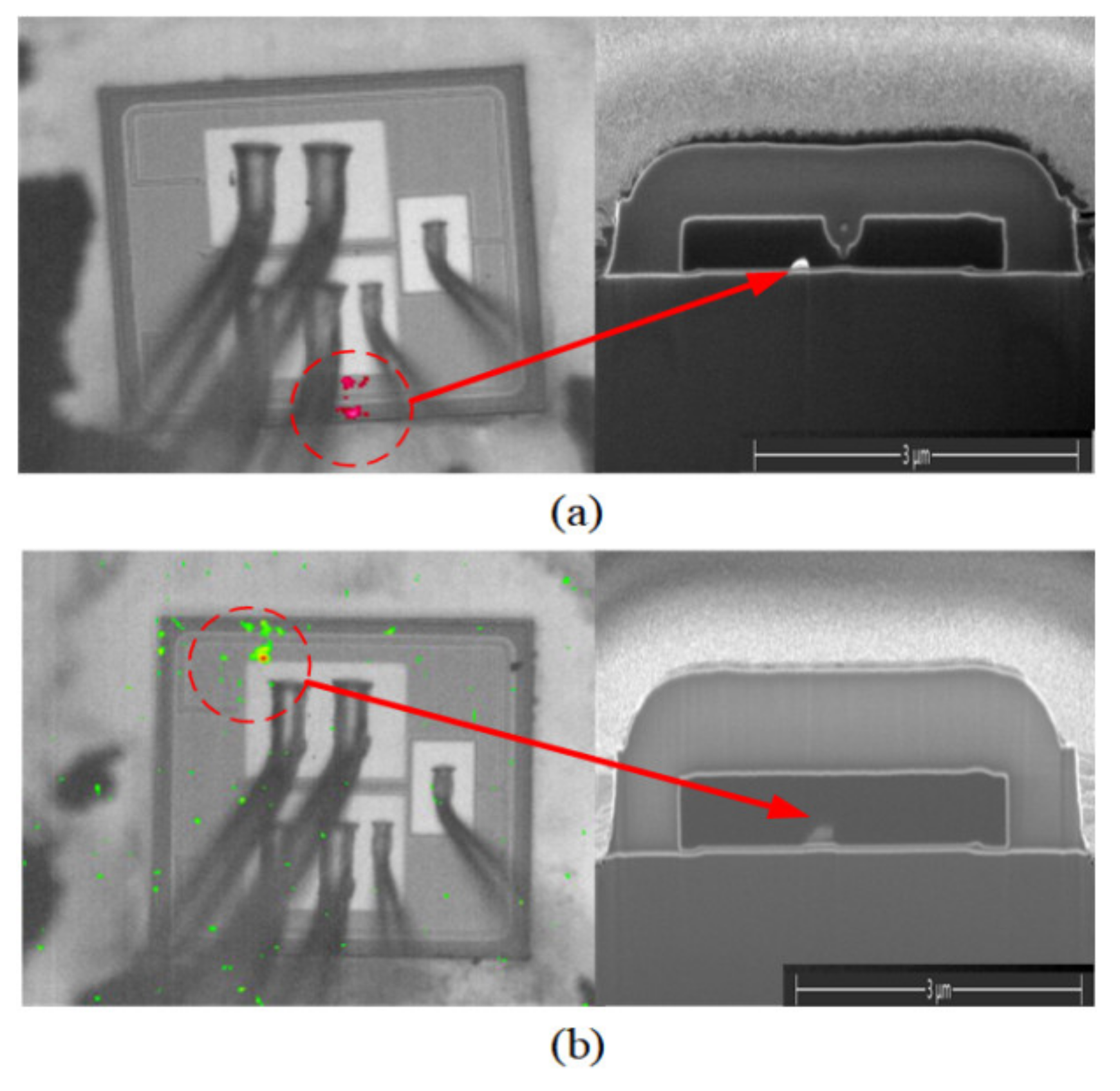
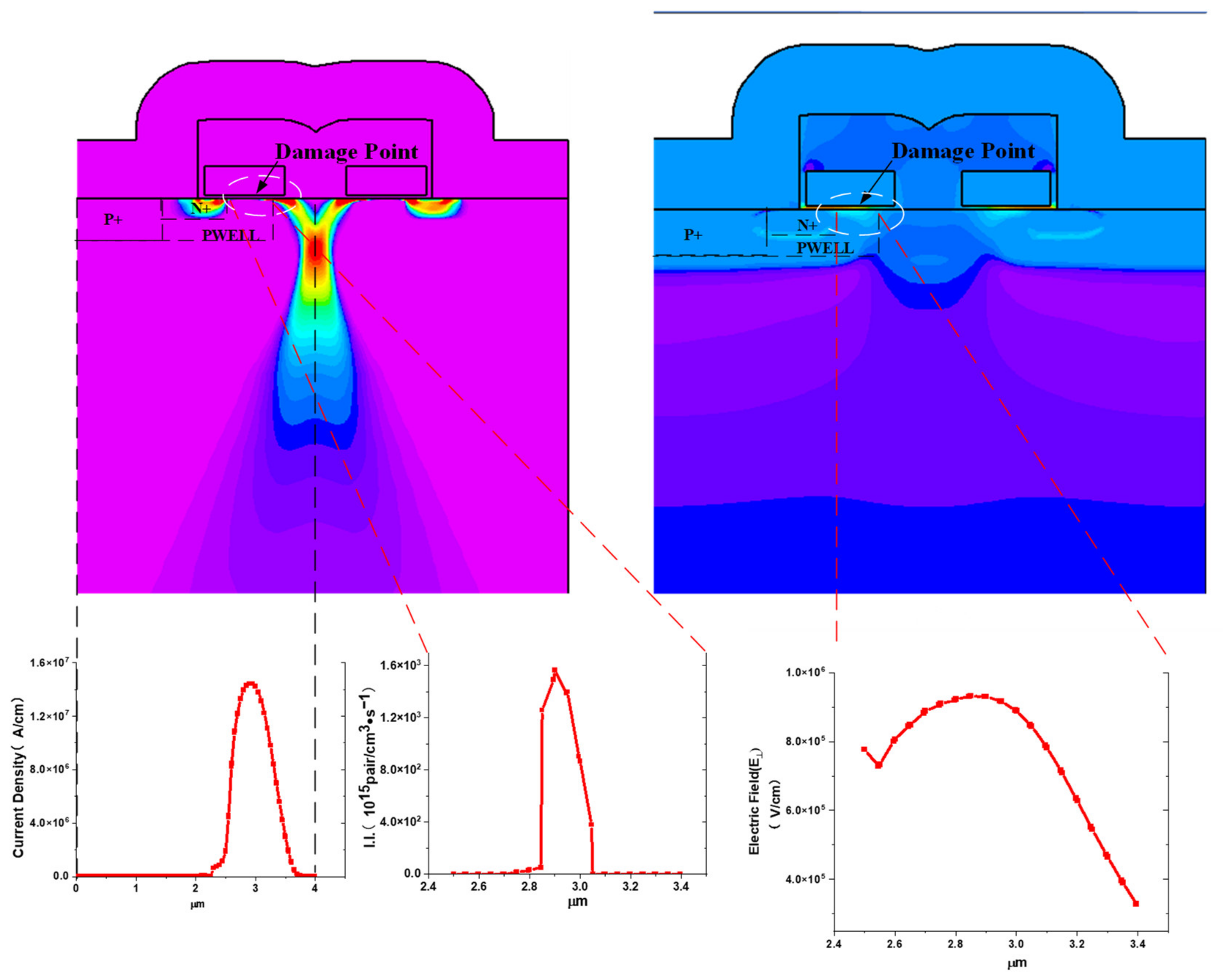
4.2. Short-Circuit Characteristics

The SC endurance capability of the SG MOSFET was also verified. The two devices were measured with a 400 V DC bus voltage at room temperature. The SC current waveforms of the PG-MOSFET and the SG-MOSFET are shown in Figure 10. The turn-on gate voltage was 20 V, along with a −5 V turn-off gate voltage [19,20]. The SC pulse width begins at 13 μs, and a 1μs increment is added for the next pulse until the device fails [6]. Between two adjacent pulses, a minute interval is allowed to cool down the device.
In Figure 10a, the short-circuit tolerance time of PG-MOSFET is 15 μs. It can be seen from the short-circuit current that the gate voltage can be turned off at 16 μs, but the short-circuit current cannot reach 250 A. To further verify the gate failure, a 17 μs test found that the gate voltage had not reached 20 V and the short-circuit current was only about 150 A. So, the device completely failed. Figure 10b shows that the short-circuit current time of SG-MOSFET is 13 μs. Although the gate voltage shows obvious fluctuation at 14 μs, the device can still be turned off at −5 V. This phenomenon indicates that the gate was damaged. When the 15 μs test is carried out, the gate cannot be turned off, and the short-circuit current exists all the time, indicating that the device has failed.
The deluding photos of the failed devices are shown in Figure 11. There is no burning mark on the surface of them, proving that the breakdown point should be inside the devices. Since the surface of the device was not burned, we located electrical leakage using an emission microscope (EMMI) and focused ion beam (FIB); the results as shown in Figure 12. Different colors were found form the gate oxide to poly where the two devices had leakage. The waveform in Figure 10 also shows that the gate oxide of the device must have been damaged; this damage could be the result of heat accumulation caused by the short circuit.
Simulation was used to reveal its mechanism. From Figure 13 and Figure 14, there is basically no difference in the current density between PG-MOSFET and SG-MOSFET. Both devices are short circuits between the gate and source. The main reason is that impact ionization and vertical electric field (E) all accumulate in the channel, which puts stress on the gate oxide.

5. Conclusions

Overall, 1.2 kV rated SiC SG-MOSFETs were successfully fabricated. It was shown that the BV of the device reaches 1600 V, the Vth is 2.65 V, the RON,sp is 5.12 mΩ cm2, and the VSD is 4.6 V. Its static electrical performance is comparable with that of the PG-MOSFET fabricated under the same process. However, the dynamic characteristics of the SG device significantly improved. The three capacitances (Ciss/Coss/Crss) reduced by 7%/8%/17%, respectively, and the Qg also reduced by 10%, indicating that the switching characteristics significantly improved. Moreover, the robustness under the UIS stresses of the two kinds of MOSFETs was analyzed. It is also shown that the UIS tolerance of PG-MOSFET is only about 5% higher than that of SG-MOSFET, which is not as much difference as was expected. Silvaco TCAD simulation was introduced to explain the reason for this, and it was found that the lattice temperatures of both devices were over 800 K when subjected to current shock, and the temperature of the Al layer also reached above 700 K melting point, which could explain the phenomenon that the Al layer melted first. After the device was impacted by a short-current test, the tolerance time of the two devices was only 2 μs apart; the SG-MOSFET did not degenerate seriously. Gate failure was found in the test waveform and the location of the damage was found by EMMI and FIB, which was consistent with the experimental phenomenon. The SiC SG-MOSFET proposed in this work improves the switching characteristics and maintains robustness, making it a promising SiC MOSFETs candidate.

Author Contributions

Conceptualization, H.L. and J.W.; methodology, H.L.; software, H.L. and Z.W.; validation, J.W., S.L. and L.S.; formal analysis, H.L.; investigation, H.L.; resources, J.W. and S.L; data curation, Z.W.; writing—original draft preparation, H.L.; writing—review and editing, J.W. and Z.W.; supervision, L.S. All authors have read and agreed to the published version of the manuscript.

Funding

This work was supported in part by the National Natural Science Foundation of China under Grant 62004037 and Grant 62174029, in part by the Fund for Transformation of Scientific and Technological Achievements of Jiangsu Province under Grant BA2020027, in part by the Research and Development Plan of Jiangsu Province under Grant BE2022073, and in part by the Important Special Project of Nanjing City under Grant 2021-11004.

Data Availability Statement

Not applicable.

Acknowledgments

The authors would like to thank SEMC for taping out and helpful discussions.

Conflicts of Interest

The authors declare no conflict of interest.

References

  1. Yoon, J.; Na, J.; Kim, K. A 1.2 kV SiC MOSFETs with Integrated Heterojunction Diode and P-shield Region. Energies 2021, 14, 8582. [Google Scholar] [CrossRef]
  2. Kimoto, T. Material science and device physics in SiC technology for high-voltage power devices. Jpn. J. Appl. Phys. 2015, 54, 040103. [Google Scholar] [CrossRef]
  3. Agarwal, A.; Han, K.; Baliga, B.J. 2.3 kV 4H-SiC Accumulation-Channel Split-Gate Planar Power MOSFETs with Reduced Gate Charge. IEEE J. Electron. Devices Soc. 2020, 8, 499–504. [Google Scholar] [CrossRef]
  4. Han, K.; Baliga, B.J.; Sung, W. Split-Gate 1.2-kV 4H-SIC MOSFETs: Analysis and Experimental Validation. IEEE Electron. Device Lett. 2017, 38, 1437–1440. [Google Scholar] [CrossRef]
  5. Yu, H.; Wang, J.; Liang, S.; Deng, G.; Liu, H.; Ji, B.; Shen, Z.J. 1.2-kV silicon carbide planar split-gate MOSFET with source field plate for superior figure-of-merits. IET Power Electron. 2022, 15, 1502–1510. [Google Scholar] [CrossRef]
  6. Han, Z.; Song, G.; Bai, Y.; Chen, H.; Liu, X.; Lu, J. A novel 4H-SiC MOSFET for low switching loss and high-reliability applications. Semicond. Sci. Technol. 2020, 35, 085017. [Google Scholar] [CrossRef]
  7. Han, K.; Baliga, B.J.; Sung, W. 1.2 kV 4H-SiC Split-Gate Power MOSFETs: Analysis and Experimental Results. Mater. Sci. Forum 2018, 924, 684–688. [Google Scholar]
  8. Yao, K.; Yano, H.; Tadano, H.; Iwamuro, N. Investigations of SiC MOSFETs Short-Circuit Failure Mechanisms Using Electrical, Thermal, and Mechanical Stress Analyses. IEEE Trans. Electron Devices 2020, 67, 4328–4334. [Google Scholar] [CrossRef]
  9. Agarwal, A.; Han, K.; Baliga, B.J. Comparison of 2.3 kV4H-SiC accumulation-channel planar MOSFETs fabricated with linear, square, hexagonal, and octagonal cell topologies. IEEE Trans. Electron Devices 2020, 67, 3673–3678. [Google Scholar] [CrossRef]
  10. Agarwal, A.; Han, K.; Baliga, B.J. 2.3 kV 4H-SiC accumulation channel JBSFETs: Experimental comparison of linear, hexagonal and octagonal cell topologies. In Proceedings of the 2020 Device Research Conference (DRC), Columbus, OH, USA, 21–24 June 2020; pp. 84–85. [Google Scholar]
  11. Baliga, B.J. Fundamentals of Power Semiconductor Devices, 2nd ed.; Springer: Cham, Switzerland, 2019; Chapter 6; pp. 283–440. [Google Scholar]
  12. Han, K.; Baliga, B.J. Comparison of four cell topologies for 1.2-kV accumulation-and inversion-channel 4H-SiC MOSFETs: Analysis and experimental results. IEEE Trans. Electron Devices 2019, 66, 2321–2326. [Google Scholar] [CrossRef]
  13. Jiang, H.; Wei, J.; Dai, X.; Ke, M.; Devany, I.; Mawby, P. SiC trench MOSFET with shielded fin-shaped gate to reduce oxide field and switching loss. IEEE Electron Device Lett. 2016, 37, 1324–1327. [Google Scholar] [CrossRef]
  14. Agarwal, A.; Han, K.J.; Baliga, B.J. Impact of cell topology on characteristics of 600 V 4H-SiC planar MOSFETs. IEEE Electron. Device Lett. 2019, 40, 773–776. [Google Scholar] [CrossRef]
  15. Xu, H.; Lin, C.; Ren, N.; Gan, X.; Liu, L.; Zhu, Z.; Liu, L.; Guo, Q.; Jiang, J.; Sheng, K. Comparison Study on Short Circuit Capability of 1.2 kV Split-Gate MOSFETs and Split-Source MOSFETs with Integrated JBS Diode. In Proceedings of the 2021 IEEE Workshop on Wide Bandgap Power Devices and Applications in Asia (WiPDA Asia), Wuhan, China, 25–27 August 2021. [Google Scholar]
  16. Han, K.; Baliga, B.J.; Sung, W. A novel 1.2 kV 4H-SiC buffered gate (BG) MOSFETs: Analysis and experimental results. IEEE Electron. Device Lett. 2018, 39, 248–251. [Google Scholar] [CrossRef]
  17. Zhu, Z.; Xu, H.; Liu, L.; Ren, N.; Sheng, K. Investigation on Surge Current Capability of 4H-SiC Trench-Gate MOSFETs in Third Quadrant Under Various VGS Biases. IEEE J. Emerg. Sel. Top. Power Electron. 2020, 9, 3028094. [Google Scholar]
  18. Tsibizov, A.; Kovačević-Badstübner, I.; Kakarla, B.; Grossner, U. Accurate Temperature Estimation of SiC Power MOSFETs under Extreme Operating Conditions. IEEE Trans. Power Electron. 2020, 35, 1855–1865. [Google Scholar] [CrossRef]
  19. Liu, J.; Zhang, G.; Wang, B.; Li, W.; Wang, J. Gate Failure Physics of SiC MOSFETs under Short-circuit Stress. IEEE Electron Device Lett. 2020, 41, 103–106. [Google Scholar] [CrossRef]
  20. Fayyaz, A.; Castellazzi, A.; Romano, G.; Riccio, M.; Irace, A.; Urresti, J.; Wright, N. Influence of gate bias on the avalanche ruggedness of SiC power MOSFETs. In Proceedings of the International Symposium on Power Semiconductor Devices and ICs, Sapporo, Japan, 28 May–1 June 2017; pp. 391–394. [Google Scholar]
Figure 1. The cross-sectional schematic views of (a) the PG-MOSFET, (b) SG-MOSFET, and (c) SEM view of the SG-MOSFET.
Electronics 12 02551 g001
Figure 2. Measured (a) forward blocking behaviors, (b) Vth curves, (c) Id-Vd characteristics with VGS from 5 V/10 V/15 V/20 V, and (d) body diode conduction characteristics with VGS = −4 V of the fabricated PG-MOSFET and SG-MOSFET.
Electronics 12 02551 g002
Figure 3. Measured three capacitances of the fabricated PG-MOSFET and SG-MOSFET (VDS = 0–800 V).
Electronics 12 02551 g003
Figure 4. Measured gate charge of the fabricated SG-MOSFET and PG-MOSFET at VDS = 800 V and ID = 20 A. The SG-MOSFET clearly shows the smaller plateau (QGD).
Electronics 12 02551 g004
Figure 5. Schematic of UIS measurement test circuit.
Electronics 12 02551 g005
Figure 6. Measured UIS waveforms of (a) the PG- MOSFET and (b) the SG-MOSFET, just before failure and when failure occurred: VGS = +20/−5 V [17].
Electronics 12 02551 g006
Figure 7. Post-failure chip surface after UIS failure at VGS = +20 V/−5 V: (a) the discontinuous digging structure split gate MOSFET; (b) the conventional planar gate MOSFET.
Electronics 12 02551 g007
Figure 8. Simulation of the UIS process of the internal lattice temperature: (a) SG-MOSFET and (b) PG-MOSFET.
Electronics 12 02551 g008
Figure 9. Simulation of the UIS process of electric field of (a) SG-MOSFET and (b) PG-MOSFET.
Electronics 12 02551 g009
Figure 10. Short-circuit current waveforms of (a) PG-MOSFET and (b) SG-MOSFET.
Electronics 12 02551 g010
Figure 11. Post-failure chip surface after short-circuit failure: (a) SG-MOSFET; (b) PG-MOSFET.
Electronics 12 02551 g011
Figure 12. SEM profile of leakage position (a) SG-MOSFET and (b) PG-MOSFEET.
Electronics 12 02551 g012
Figure 13. Current density, impact ionization, and vertical electric field (E⊥) under SG-MOSFET structure simulation.
Electronics 12 02551 g013
Figure 14. Current density, impact ionization, and vertical electric field (E⊥) under PG-MOSFET structure simulation.
Electronics 12 02551 g014
Table 1. Design parameters for PG-MOSFET and SG-MOSFET.
ParametersSG-MOSFETPG-MOSFET
Tdrift/Ndrift10 μm/9 × 15 cm−310 μm/9 × 15 cm−3
NCSL1 × 17 cm−31 × 17 cm−3
TPbase/NPbase0.7 μm/1 × 18 cm−30.7 μm/1 × 18 cm−3
LCH0.4 μm0.4 μm
WJEFT1.8 μm1.8 μm
Sox1.5 μm × 0.5 μm-
WCELL8.2 μm8.2 μm
Table 2. Summary of experiment results for PG-MOSFET and SG-MOSFET.
ParametersPG-MOSFETSG-MOSFETChange
Threshold voltage (V)2.62.652%
RON (mΩ)78.1802%
RON(SP) (mΩ·cm2)55.122.4%
Breakdown voltage (V)160916090%
VSD@VGS = −4 V4.64.60%
Ciss@VDS = 0 V (pF)207319326.8%
Coss@VDS = 0 V (pF)223720687.6%
Crss@VDS = 0 V (pF)91475617.3%
Qg(nC)@VGS = 20 V807210%
Disclaimer/Publisher’s Note: The statements, opinions and data contained in all publications are solely those of the individual author(s) and contributor(s) and not of MDPI and/or the editor(s). MDPI and/or the editor(s) disclaim responsibility for any injury to people or property resulting from any ideas, methods, instructions or products referred to in the content.

