
Design of a 2.4 & 5.8 GHz Efficient Circularly Polarized Rectenna for Wireless Power Transfer Applications

School of Information and Electronic Engineering, Zhejiang Gongshang University, Hangzhou 310000, China
*
Authors to whom correspondence should be addressed.
Electronics 2023, 12(12), 2645; https://doi.org/10.3390/electronics12122645
Submission received: 26 April 2023
/
Revised: 9 June 2023
/
Accepted: 10 June 2023
/
Published: 12 June 2023
(This article belongs to the Special Issue Recent Advances in RF and Millimeter-Wave Design Techniques)
Abstract
:In this paper, we proposed a novel dual-band circularly polarized rectifier antenna for collecting environmental electromagnetic energy at 2.4 and 5.8 GHz. The receiving antenna is a circularly polarized microstrip slot antenna that achieves circular polarization in the low-frequency band (2.4 GHz) and high-frequency band (5.8 GHz) through the use of the “U” slot of the ground and the “L” branch of the upper patch, respectively. The antenna exhibits impedance bandwidths of 320 MHz (2.18–2.50 GHz) and 3.73 GHz (5.33–9.06 GHz) in the 2.4 GHz and 5.8 GHz bands, respectively, while the 3 dB axis specific bandwidths are 260 MHz (2.32–2.58 GHz) and 420 MHz (5.66–6.08 GHz), respectively. The antenna gains are 3.5 dBi and 6.2 dBi at 2.4 GHz and 5.8 GHz, respectively. Furthermore, a dual-frequency voltage doubling rectifier circuit was designed to operate with the antenna. A dual-branch matching circuit was used to achieve impedance matching between the antenna and the rectifier circuit, and the output was optimized to suppress high-order harmonics through sector branches to improve the rectification efficiency. The simulation results show that the maximum rectification efficiency of the circuit is more than 80%, with a measured efficiency of over 60%. This 2.4–5.8 GHz dual-band circularly polarized rectifier antenna has the potential to self-power low-power devices in the Internet of Things, making it a valuable contribution to the field of wireless energy harvesting.
1. Introduction
With the rapid development of new generation communication technologies such as 5G [1,2,3], we have entered the era of the Internet of Things (IoT), where everything is interconnected. Mobile phones, tablets, and smart wearable devices [4] are being used more and more widely in people’s daily lives. However, the use of a large number of sensors in wireless sensor networks (WSNs) inevitably leads to the problem of power supply. Despite the current maturity of battery technology, battery power supply still faces several issues, such as high cost, high maintenance costs, and environmental concerns [5,6]. Furthermore, advances in integrated circuit technology have resulted in the lower power consumption of electronic devices, making it possible to supply devices wirelessly through electromagnetic signals. However, due to the complex wireless energy transmission environment, effectively collecting and receiving radio frequency energy poses a design challenge. Therefore, efficient recovery of environmental electromagnetic energy is of great significance [7].
The rectifier antenna is a crucial component for harvesting electromagnetic energy, consisting of both a receiving antenna and a rectifying circuit. Sun et al. [8] proposed a rectifier antenna operating at 2.45 GHz, which achieves 73.9% conversion efficiency at a receiving power of 10.4 dBm. Indeed, the energy in the environment is not limited to a single band of radio frequency energy. Therefore, rectifier antennas with broadband or multiband capability can have a better energy collection effect. The 1.8–2.5 GHz broadband rectifier antenna proposed by Song et al. [9] can achieve over 40% rectification efficiency at an input power of 20 dBm. Nie et al. [10] designed a GCPW (Grounded Coplanar Waveguide) feed broadband rectifier antenna, which can have over 50% energy conversion efficiency in the 2.2–2.6 GHz band when the receiving power is 13 dBm. Paper [9,10] has good rectification efficiency but is not suitable for low input power density environments. Chandravanshi et al. [11] designed a 2, 2.5, 3.5 GHz three-band differential rectifier antenna which can achieve 53%, 31%, and 15.56% rectification efficiency at −12 dBm reception power, respectively. A. Mavaddat et al. [12] implemented a 4 × 4-cell rectifier array using a rectangular patch antenna, which achieves 67% energy conversion efficiency when the input power is 7 mW. The author is currently aware that Naoki Sakai et al. [13] used a high impedance folded dipole antenna (FDA) as the receiving antenna. The rectifier circuit uses a special GaAs Schottky diode bridge packaging chip as the core of the rectifier circuit. When the input power is 32 dBm, the rectifier efficiency reaches 92.8% but the antenna can also not work effectively in low input power environment. It is evident that the design of multiband rectifier antennas as well as low input power rectifier antennas poses a significant challenge.
This research paper presents a novel dual-band rectifier antenna designed to efficiently collect electromagnetic energy in low-power environments. The antenna operates in the 2.4–5.8 GHz band and uses a circularly polarized microstrip slot antenna as the receiving element. Circular polarization was preferred over linear polarization due to its better environmental adaptability and penetration, resulting in higher energy conversion efficiency. The dual-branch matching network ensures good impedance matching between the receiving antenna and the rectifier circuit in both the 2.4 GHz and 5.8 GHz bands. The output was also optimized to suppress high-order harmonics through the use of a sector branch, thereby improving the efficiency of energy conversion. The simulation and test results demonstrated that the designed rectifier antenna has good rectification efficiency in both the 2.4 GHz and 5.8 GHz bands, making it suitable for self-powering low-power devices in the Internet of Things.
2. Receiving Antenna Structure and Parameters
The conventional rectifier antenna typically utilizes a linear polarized antenna. However, the radio frequency energy in the environment is characterized by its complexity and variability [13,14]. Linear polarized receiving antennas tend to incur polarization loss and single frequency antenna can only efficiently collect radio frequency energy of a single band, whereas the energy in the environment cannot be restricted to a single band. As a solution, a high efficiency dual-band circularly polarized rectifier antenna was proposed in this study.
To provide clarity on the design process of the dual-frequency circularly polarized antenna, Figure 1 is presented. The antenna was designed using RO4350B as the dielectric substrate with a relative dielectric constant of 3.66, a thickness of 1.524 mm, and a tangent of the loss angle of 0.0037.
Figure 2 shows the S11 parameter frequency response curve and the 3-dB axis ratio bandwidth frequency response curve of antennas 1, 2, 3, 4. Ant.1 is a traditional printed linear polarized microstrip slot antenna. The patch located on the upper layer of the dielectric substrate was used to achieve high frequency radiation. The resonant path of the upper band was (). The path length should be one-fourth of the dielectric wavelength of the high frequency band. The rectangular slot on the floor was used for radiation in the low frequency band. The perimeter of the rectangular slot is the dielectric wavelength of the low frequency band.
The size of the upper strip can be obtained using Formula (1). However, Ant.1 exhibits multiband radiation and can only cover up to 2.4 GHz at low frequencies. The resonant point at high frequencies is lower than the desired 5.8 GHz for the antenna design. Ant.2 is an improvement on Ant.1, which adds an “L” type metal strip to the upper patch and a rectangular strip to the floor to form a “U” type slot. The “L” strip achieves resonance in the high frequency band and improves circular polarization in the same band by changing the current path. The “U” slot achieves circular polarization in the low frequency band. However, the resonance point in the low frequency band decreases and 2.4 GHz is not located in the impedance bandwidth in the low frequency band. Figure 2a shows that the impedance bandwidth in the high frequency band has improved significantly. Figure 2b shows that the antenna has a circularly polarized radiation trend in the high frequency band due to the introduction of the “L” strip but the axis ratio in the low frequency band is still greater than 3 dB. Ant.3 improves upon Ant.2 by eliminating the semi-circular metal part of the upper metal strip. This modification results in several benefits, such as reducing the discontinuity of the upper metal strip, improving radiation efficiency, increasing its width, and optimizing impedance matching. In addition, two chamfered Rf2 were added to the slotted floor and two chamfered Rf1 were added to the rectangular strip, with all four chamfered radii being 5 mm. The purpose of these chamfered radii was to enhance the circular polarized radiation in the low frequency band. As shown in Figure 2a, Ant.3 achieves the desired impedance bandwidth, effectively covering the 2.4 GHz and 5.8 GHz bands. Moreover, circular polarization radiation is observed in the low frequency band, effectively covering the 2.4 GHz band, with 5.8 GHz serving as the center point of the 3 dB axis ratio bandwidth in the high frequency band. Ant.3 has successfully met the requirements of dual-band circular polarization radiation at 2.4/5.8 GHz. Thus, the antenna optimized by Ant.3 has basically satisfied the requirements for dual-frequency circularly polarized radiation. Ant.4 mainly optimizes Ant.3 further, the microstrip feeder is 2.5 mm, the first chamfered Rf3 = 5 mm on the upper patch to optimize the axis ratio bandwidth; then, by introducing a small stripline to optimize impedance, which is d3 = 1 mm away from the patch, long Lp = 2 mm, and 0.8 mm wide. From Figure 2a, it can be seen that Ant.4 has further improved impedance matching on the basis of Ant.3, whether in high or low frequency bands. From Figure 2b, it can be seen that Ant.4 has a better 3-dB axis ratio bandwidth than Ant.3. The final optimized size of the antenna is shown in Table 1.
2.1. Antenna Radiation Principle
In order to explain the radiation principle of the designed antenna in more detail, Figure 3 shows the simplified equivalent circuit model diagram of the circularly polarized microstrip slot antenna. The circuit model of Figure 3 qualitatively reproduces the impedance locus of the antenna. The uncoupled patch and slot resonators were explicitly coupled through a mutual inductance. This was justified given that a slot voltage is proportional to the time-derivative of the current it intercepts; in this case, the antenna can be thought of as intercepting the mode patch current. The mutual inductance is , where ; given the CMA mode 1 and 3 resonant frequencies, it yields . For each resonator, RLC values may be calculated from the uncoupled resonator CMA data (, and Q) via circuit analysis [15]:
where .
Meanwhile, in order to better separate the 2.4 GHz and 5.8 GHz operating frequency bands and reduce the coupling effect between the two frequency bands, Figure 4 shows the surface current distribution of the antenna at 2.4 GHz and 5.8 GHz. Through current vector synthesis, it can be seen that the antenna exhibits right-handed circularly polarized radiation at 2.4 GHz and left-handed circularly polarized radiation at 5.8 GHz.
2.2. Antenna Parameter Scanning Analysis
To investigate the sensitivity of the impedance bandwidth and 3-dB circularly polarized axis ratio bandwidth of dual-band circularly polarized microstrip slot antennas to key parameters, a detailed analysis of important parameters was conducted. During the optimization process, only the parameters that were being analyzed were varied, while other important parameters were set to their optimized values [16]. The performance of the dual-frequency circularly polarized microstrip slot antenna was primarily dependent on the length of the “L” strip of the upper patch and the parameters of the rectangular strip on the slotted floor. Specifically, antenna performance parameters were mainly related to L2, W2, L3, and L4 values, and therefore, these four parameters were the main focus of study and analysis.
Figure 5a illustrates the effect of parameter L2 on the performance of the antenna. The plot indicates that as L2 decreases, the S11 parameter of the antenna improves in the low frequency band. Specifically, when L2 is set to 19 mm, the S11 impedance bandwidth of the antenna in the low frequency band is 230 MHz (2.27–2.5 GHz), with an S11 value of −15 dB at 2.4 GHz. On the other hand, when L2 is set to 15 mm, the impedance bandwidth of the antenna in the low frequency band increases to 350 MHz (2–2.55 GHz), with an S11 value at 2.4 GHz of −22 dB. Figure 5b demonstrates that the optimal 3-dB axis ratio bandwidth of the antenna in the low frequency band occurs at L2 = 17 mm, whereas the optimal 3-dB axis ratio bandwidth in the high frequency band is achieved when L2 = 15 mm. Considering both frequency bands, an L2 value of 17 mm was chosen as it fully satisfied the requirements. Overall, the L2 parameter has a minimal impact on the antenna’s S11, but it has a more significant effect on the 3-dB axis ratio bandwidth.
Figure 6a depicts the impact of W2, a parameter that affects antenna performance. As shown in the figure, decreasing W2 shifts the antenna’s resonance frequency to lower frequencies. However, when W2 is reduced beyond a certain value, this shift is no longer apparent. Instead, there is a notable change in S11 at 2.4 GHz. The effect of W2 on S11 at high frequencies is minor and remains within acceptable limits. This is because the upper metal patches primarily determine antenna performance in this frequency range, and the lower ground has a minimal role. Figure 6b illustrates that decreasing W2 causes the 3-dB axis of the low-frequency band to shift from the high-frequency region to the low-frequency region, relative to the bandwidth center. Conversely, the 3 dB axis of the high-frequency band moves from the low-frequency range to the high-frequency range. Therefore, to optimize performance in both frequency ranges, a W2 value of 30 mm is recommended. This value yields a 3-dB axis of 2.45 GHz in the low-frequency band and a 3-dB axis of 5.8 GHz in the high-frequency band, relative to the bandwidth center. Thus, the W2 value is optimized at 30 mm, which is close to the two center frequency points of the antenna design.
Figure 7 illustrates the impact of parameter L3 on the antenna’s performance. It can be observed from Figure 7a that for L3 = 10 mm, the antenna’s resonance frequency in the low frequency band is close to the design frequency of 2.45 GHz. However, with the increase in L3, the resonance frequency point of the antenna in the high frequency band and its bandwidth shift towards the low frequency band. Figure 7b shows that, when L3 = 12 mm, the antenna’s 3-dB axis ratio bandwidth center point in the low frequency band is near 2.2 GHz, while in the low frequency band, it is only at 2.4 GHz when L3 = 10 mm. In addition, when L3 goes from 8 mm to 10 mm, the antenna’s 3-dB axis in the high frequency band shifts towards a high frequency with the increase in L3 compared to the bandwidth center point. However, when L3 is 10 mm, the antenna’s 3-dB axis in the high frequency band is close to 5.8 GHz. Although the antenna’s 3-dB axis has a better bandwidth ratio when L3 is 10 mm compared to L3 = 12 mm, it is not effective in covering the 5.8 GHz WiFi band, and its performance in the low frequency band is also unsatisfactory. Hence, parameter L3 is optimized at 10 mm.
From Figure 8a, it can be seen that the impedance bandwidth of the antenna moves towards the high frequency band with the decrease of L4. The impedance bandwidth of the antenna in the low frequency band can only cover the WiFi band at 2.4 GHz when L4 = 5 mm. Figure 8b shows that, with the decrease of L4, the antenna’s 3-dB axis ratio bandwidth and the axis ratio bandwidth center point move towards the high frequency band in both the high and low frequency bands. When L4 = 7 mm, the antenna’s 3-dB axis ratio bandwidth center point in the low and high frequency bands is 2.3 GHz and 5.75 GHz, respectively, while when L4 = 3 mm, the axis ratio bandwidth center point is 2.65 GHz and 5.9 GHz, respectively. Only when L4 = 5 mm, the 3-dB axis ratio bandwidth center point is around 2.4 GHz and 5.8 GHz, respectively. Therefore, parameter L4 was optimized to 5 mm for the best antenna performance.
2.3. Directional Pattern Analysis of Dual-Frequency Circularly Polarized Microstrip Slot Antenna
Figure 9 shows the pattern of the dual-band circularly polarized microstrip slot antenna at 2.4 GHz. The pattern of the designed antenna at 2.4 GHz is similar to that of the dipole antenna, with maximum gain at and degrees, and a maximum gain of 3.5 dBi, which is higher than that of the traditional dipole antenna. Figure 9b shows the relationship between the gain and frequency of the dual-band circularly polarized microstrip slot antenna in the low frequency band (2.4 GHz). From the diagram, it can be seen that the antenna has more than 3.3 dBi gain in the 2–3 GHz range, and the antenna has more than 3.5 dBi gain in the 2.14–2.53 GHz range.
Figure 10 shows the pattern of the antenna at 5.8 GHz. As the circular polarization radiation in the high frequency band is mainly determined by the upper metal patch structure, the radiation pattern of the antenna at the 5.8 GHz high frequency band is omnidirectional, and the maximum gain of the antenna at 5.8 GHz is 6.2 dBi. As the upper metal patch is along the x-axis, the radiation gain of the antenna at degrees is greater than that at degrees. Figure 10b shows the relationship between the antenna’s radiation gain and frequency in the high frequency band. From the graph, it can be seen that the antenna has more than 5.25 dBi gain in the 5–7 GHz band range, and the antenna has more than 6 dBi gain in the 5–5.95 GHz band range.
3. Design of Rectifier Circuit
The previously designed dual-band microstrip slot circularly polarized antenna primarily receives radio frequency energy, which needs to be converted to DC power supply using a rectifier circuit [16]. To this end, a high-efficiency voltage doubling rectifier circuit was designed, as shown in Figure 11. The input is matched to the antenna via a two-branch matching circuit. The rectifier diode uses Schottky barrier diodes HSMS-2862 (D1 and D2) with zero bias voltage, a single diode series resistance of 5 , a junction capacitance of 0.18 pF, a reverse breakdown voltage of 7 V, and a reverse breakdown current of 100 mA [17,18]. The output suppresses high-order harmonics through a sector branch to improve rectification efficiency. Capacitance C1 is primarily used to prevent the DC component generated during rectification from backtracking to the circularly polarized receiving antenna, thereby reducing energy loss. Capacitance C2 acts as both a filter capacitor and a storage capacitor [19]. It determines the setup time and jitter amplitude of the output voltage. The larger the capacitance, the larger the charge constant , resulting in a longer time for the output voltage to reach steady-state. However, it also makes the output voltage more stable [20]. Both capacitors C1 and C2 are Murada GQM series high frequency capacitors with a capacity of 100 pF.
3.1. Design of Output Low-Pass Filter
The output low-pass filter is primarily composed of two sector-shaped microstrip branches angled at 120 degrees. In the radio frequency band, the sector branch is equivalent to a lumped capacitance. The sector branch is cascaded with its 50 ohm microstrip line in front of it to form an RC low-pass filter, which can effectively suppress harmonics. The transmission matrix A [21] of a microstrip line with a length of one-quarter wavelength is given by Formula (4):
It is visible that a quarter-wavelength transmission line can perform an impedance or admittance inversion transformation, and hence it can be treated as a K or J converter, where or . As a result, the capacitive impedance can be transformed into inductive impedance [22], an open circuit can be transformed into a short circuit, and a short circuit can be transformed into an open circuit. Additionally, can be transformed into = ∝ through the function of a K or J converter [23]. The rectifier circuit employs two sector branches to suppress high-frequency harmonics at 5.8 GHz and low-frequency harmonics at 2.4 GHz, respectively. The optimized size of the sector branches was determined using ADS2020 software. The initial radius of the smaller sector branch was set to one-fourth of the 5.8 GHz wavelength, while the radius of the larger sector branch was set to one-fourth of the 2.4 GHz wavelength. The primary objective of the output low-pass filter is to suppress the primary harmonics in both the low and high frequency bands while minimizing the overall size of the rectifier circuit.
Figure 12 illustrates the S11 parameter curve of the output low-pass filter. The S11 parameters of the first harmonic (2.4 GHz) and second harmonic (4.8 GHz) in the low frequency band are −0.007 dB and −0.058 dB, respectively. This indicates that the designed low-pass filter effectively suppresses both the first and second harmonics in the low frequency band, preventing their transmission to the load side. In the high frequency band, the S11 parameters of the output low-pass filter are −0.082 dB and −0.183 dB for the first harmonic (5.8 GHz) and second harmonic (11.6 GHz), respectively. This indicates that the output low-pass filter also suppresses the harmonic component in the high frequency band, leading to an improved rectification efficiency of the double-frequency rectifier circuit.
3.2. Design of Matching Circuit
There are three main functions of a matching circuit [24]:
- The RF energy of the working frequency of the rectifier circuit, that is, the base wave energy, passes through, prevents the second and higher harmonics generated by the diode from passing through, and reflects the harmonics back to the diode.
- Impedance matching between the receiving antenna and the rectifier diode is achieved, which prevents the energy received by the diode from entering the rectifier diode completely for rectification, which results in incomplete RF energy rectification and reduced rectification efficiency of the rectifier circuit.
- Prevents some irrelevant RF energy from entering the diode of the receiving antenna, thereby affecting the rectification efficiency of the main rectifier band.
Figure 13a illustrates that both the real and imaginary parts of the diode’s input impedance increase with the input frequency. In the low frequency band (2.4 GHz), the real part of the input impedance is close to 50 ohm, which differs significantly from the 50 ohm impedance in the high frequency band (5.8 GHz). Additionally, the imaginary part of the impedance shows capacitance in the low frequency band and inductance in the high frequency band. To simplify the dual-frequency matching circuit, a short-circuit microstrip line was added in series to the D2 segment of the diode, which is one-eighth of the 5.8 GHz wavelength. This microstrip line not only suppresses harmonics but also compensates the diode’s impedance in the high-frequency band, balancing the impedance of the low-frequency band with that of the high-frequency band and improving the dual-frequency matching. Moreover, Figure 13b shows that the diode’s impedance changes significantly when the input power is low and only becomes relatively stable when the input power exceeds 5 dBm. Therefore, considering the risk of diode breakdown due to high input power, the optimal design selects an input power of 10 dBm.
Figure 14 depicts the optimized S11 parameter curve of the rectifier circuit. The curve indicates that the S11 parameter at 2.4 GHz in the low frequency band is −17 dB, and the impedance bandwidth at the low frequency band is 270 MHz (2.25–2.52 GHz). Similarly, the S11 parameter at 5.8 GHz in the high frequency band is −31 dB, and the impedance bandwidth at the high frequency band is 400 MHz (5.71–6.11 GHz). Thus, the designed matching circuit satisfies the requirements of the two WiFi bands, 2.4 GHz and 5.8 GHz, thereby enabling the rectifier circuit to effectively rectify signals in both frequency bands.
3.3. Analysis of Simulation Results of Rectifier Circuit
The simulation results of the analysis of the rectifying efficiency of the rectifier circuit can be obtained using Formula (5). The is the DC output voltage, is the load resistance, is the input RF power.
Figure 15 displays the rectification efficiency versus the input power curve for the rectifier circuit. The graph shows that the rectification efficiency at 2.4 GHz is higher compared to that at 5.8 GHz, which is consistent with the output DC voltage versus the input power curve. Additionally, at the input frequency of 2.4 GHz, the rectifier circuit achieves the highest efficiency of 88% at an input power of 14 dBm and maintains over 60% efficiency in the input power range of 3 dBm to 16 dBm. Similarly, at the input frequency of 5.8 GHz, the rectifier circuit achieves the highest efficiency of 81% at an input power of 10 dBm and maintains over 60% efficiency in the input power range of 7 dBm to 12 dBm.
4. Experimental Results
In this paper, we conducted physical testing on the dual-frequency voltage rectifier circuit. The circuit had a physical size of mm and was constructed using an RO4350B high-frequency plate as the dielectric base. The HS286C type diode, encapsulated with SOT-323, was used in the circuit along with a load resistance of 1800 ohm. The capacitance C1 and C2 were Murada high frequency GQM series capacitors with a capacitance value of 10 pF. Figure 16 shows a physical testing diagram of the rectifier circuit where an RF signal source was used as the energy source, and the RF energy was transmitted to the rectifier circuit through an SMA connector and a 50 ohm transmission line. The rectifier circuit successfully converted the RF energy to DC energy.
Figure 17 displays the output power of the RF signal source utilized during the 2.4 GHz and 5.8 GHz tests. Meanwhile, Figure 18 presents the simulation and physical test outcomes of the output DC voltage. It is evident that the test results in the 2.4 GHz frequency band align closely with the simulation results. However, there is a notable discrepancy between the test and simulation outcomes in the 5.8 GHz frequency band. This is primarily attributed to the reduced performance of the diode at high frequencies. As stated in the official HSMS286C diode documentation, its highest operating frequency is only 5.8 GHz. Thus, the actual soldered diode may not perform optimally in the high-frequency range.
Figure 19 illustrates the optimal rectification efficiency of the physical test at 2.4 GHz and 5.8 GHz. Table 2 provides a comparison between the test results and the simulation results. The experimental results demonstrate a rectification efficiency exceeding 60% in both frequency bands, indicating a significant rectification effect.
Moreover, from Table 3, it can be seen that the rectifier circuit designed in this article can achieve a rectification efficiency of over 60% under lower input power conditions; a DC voltage output of 3.71 V was obtained at 2.4 GHz, which can be directly applied to some low-power devices. Although there is only a 2.82 V DC voltage output in the 5.8 GHz frequency band, combined with the energy management module, good results can still be achieved. It can be seen that the rectifier circuit designed in this article has a good reference value.
5. Conclusions
This article proposed a novel high-efficiency dual-band (2.4 and 5.8 GHz) circularly polarized rectifying antenna. The antenna section employed a circularly polarized antenna that effectively reduced polarization loss, while the circuit section utilized a fan-shaped harmonic suppression structure and a voltage-doubler rectification structure to enhance energy conversion efficiency. The receiving antenna achieved circularly polarized radiation in the high-frequency band (5.8 GHz) through the upper-layer patch “L”-shaped branch, and circularly polarized radiation in the low-frequency band (2.4 GHz) through a ground floor “U”-shaped slot. The circular polarization bandwidth was improved by optimizing the current path through rounded corners. Additionally, a small microstrip line was used on the feed line to improve impedance matching. The rectification circuit compensates for the input impedance of the rectifying diode using a short-circuit microstrip line. The input end was matched with a dual-branch matching network to achieve dual-band matching, while the output end effectively suppressed higher-order harmonics using a fan-shaped branch to improve rectification efficiency. The experimental results showed conversion efficiencies of 79.3% and 60.0% at the 2.4 GHz and 5.8 GHz frequency points, respectively. This rectifying antenna has the advantages of high conversion efficiency, simple structure, and easy integration, making it particularly suitable for low-power Internet of Things electronic devices.
Author Contributions
Author Conceptualization and writing—original draft, resources, X.D.; simulation, X.D.; Physical welding and testing, X.D., P.Y. and S.C.; review and editing and validation, X.D., P.Y., S.C. and W.R. All authors have read and agreed to the published version of the manuscript.
Funding
This research was supported by Basic Public Welfare Research Plan and Natural Science Foundation of Zhejiang Province under Grant No. LGG19F010005.
Data Availability Statement
The data used to support the findings of this study are included within the article.
Acknowledgments
Special thanks go to Ling Cai for permission to use the Power Electronics Equipment.
Conflicts of Interest
The authors declare no conflict of interest.
References
- Roselli, L.; Carvalho, N.B.; Alimenti, F.; Mezzanotte, P.; Orecchini, G.; Virili, M.; Mariotti, C.; Goncalves, R.; Pinho, P. Smart surfaces: Large area electronics systems for Internet of Things enabled by energy harvesting. Proc. IEEE 2014, 102, 1723–1746. [Google Scholar] [CrossRef]
- Boaventura, A.J.S.; Carvalho, N.B. A batteryless RFID remote control system. IEEE Trans. Microw. Theory Tech. 2013, 61, 2727–2736. [Google Scholar] [CrossRef]
- Zhao, J.; Subramanyam, G.; Yue, H. A dual-band rectifying antenna design for RF energy harvesting. In Proceedings of the 2020 IEEE 63rd International Midwest Symposium on Circuits and Systems (MWSCAS), Springfield, MA, USA, 9–12 August 2020; pp. 415–418. [Google Scholar] [CrossRef]
- Soumaya, A.; Mounir, R.; Terchoune, H.; Zbitou, J. High Efficiency Rectifier Circuit for Ambient RF Energy Harvesting Applications at 5.8 Hz. In Proceedings of the 2019 IEEE 7th Mediterranean Congress of Telecommunications (CMT), Fez, Morocco, 24–25 October 2019; pp. 1–5. [Google Scholar] [CrossRef]
- An, C.; Ryu, H.G. Efficient microwave power transfer system using retrodirective antenna array. Int. J. Electron. 2023, 110, 391–403. [Google Scholar] [CrossRef]
- Lin, W.; Ziolkowski, R.W. High performance electrically small Huygens rectennas enable wirelessly powered Internet of Things sensing applications: A review. Engineering 2022, 11, 42–59. [Google Scholar] [CrossRef]
- Dang, K.; Liu, H.; Zhang, C.; Huo, S.; Zhan, P.; Qiu, Z.; Zhang, Y.; Zhou, H.; Ning, J.; Zhang, J.; et al. First Demonstration of Watt-Level C-Band MMIC Rectifier With GaN Schottky Diode. IEEE Microw. Wirel. Technol. Lett. 2023, 33, 591–594. [Google Scholar] [CrossRef]
- Sun, H. An Enhanced Rectenna Using Differentially-Fed Rectifier for Wireless Power Transmission. IEEE Antennas Wirel. Propag. Lett. 2016, 15, 32–35. [Google Scholar] [CrossRef]
- Song, C.; Huang, Y.; Zhou, J.; Carter, P.; Yuan, S.; Xu, Q.; Fei, Z. Matching Network Elimination in Broadband Rectennas for High-Efficiency Wireless Power Transfer and Energy Harvesting. IEEE Trans. Ind. Electron. 2017, 64, 3950–3961. [Google Scholar] [CrossRef] [Green Version]
- Nie, M.J.; Yang, X.X.; Tan, G.N.; Han, B. A Compact 2.45-GHz Broadband Rectenna Using Grounded Coplanar Waveguide. IEEE Antennas Wirel. Propag. Lett. 2015, 14, 986–989. [Google Scholar] [CrossRef]
- Chandravanshi, S.; Sarma, S.S.; Akhtar, M.J. Design of Triple Band Differential Rectenna for RF Energy Harvesting. IEEE Trans. Antennas Propag. 2018, 66, 2716–2726. [Google Scholar] [CrossRef]
- Mavaddat, A.; Armaki, S.H.M.; Erfanian, A.R. Millimeter-Wave Energy Harvesting Using 4*4 Microstrip Patch Antenna Array. IEEE Antennas Wirel. Propag. Lett. 2014, 14, 515–518. [Google Scholar] [CrossRef]
- Sakai, N.; Noguchi, K.; Itoh, K. A 5.8-GHz band highly efficient 1-W rectenna with short-stub-connected high-impedance dipole antenna. IEEE Trans. Microw. Theory Tech. 2021, 69, 3558–3566. [Google Scholar] [CrossRef]
- Niotaki, K.; Kim, S.; Jeong, S.; Collado, A.; Georgiadis, A.; Tentzeris, M.M. A compact dual-band rectenna using slot-loaded dual band folded dipole antenna. IEEE Antennas Wirel. Propag. Lett. 2013, 12, 1634–1637. [Google Scholar] [CrossRef]
- Borchardt, J.J.; Lapointe, T.C. U-slot patch antenna principle and design methodology using characteristic mode analysis and coupled mode theory. IEEE Access 2019, 7, 109375–109385. [Google Scholar] [CrossRef]
- Ren, Y.J.; Chang, K. 5.8-GHz circularly polarized dual-diode rectenna and rectenna array for microwave power transmission. IEEE Trans. Microw. Theory Tech. 2006, 54, 1495–1502. [Google Scholar] [CrossRef]
- Mansour, M.M.; Kanaya, H. Novel L-slot matching circuit integrated with circularly polarized rectenna for wireless energy harvesting. Electronics 2019, 8, 651. [Google Scholar] [CrossRef] [Green Version]
- Li, Y.; Lu, Z.; Yang, L. CPW-fed slot antenna for medical wearable applications. IEEE Access 2019, 7, 42107–42112. [Google Scholar] [CrossRef]
- Divarathne, C.; Karmakar, N. A maximum likelihood based tag detection technique for MIMO chipless RFID systems. In Proceedings of the 2014 IEEE International Microwave and RF Conference (IMaRC), Bangalore, India, 15–17 December 2014; pp. 5–8. [Google Scholar] [CrossRef]
- Zhang, Q.; Ou, J.H.; Wu, Z.; Tan, H.Z. Novel microwave rectifier optimizing method and its application in rectenna designs. IEEE Access 2018, 6, 53557–53565. [Google Scholar] [CrossRef]
- Chen, Y.Y.; Jiao, Y.C.; Zhao, G.; Zhang, F.; Liao, Z.L.; Tian, Y. Dual-band dual-sense circularly polarized slot antenna with a C-shaped grounded strip. IEEE Antennas Wirel. Propag. Lett. 2011, 10, 915–918. [Google Scholar] [CrossRef]
- Shariati, N.; Rowe, W.S.; Scott, J.R.; Ghorbani, K. Multi-service highly sensitive rectifier for enhanced RF energy scavenging. Sci. Rep. 2015, 5, 9655. [Google Scholar] [CrossRef] [Green Version]
- Rajawat, A.; Suri, K.; Mohta, M. Design of an efficient rectifier circuit based on karthaus-fischer voltage multiplier for energy harvesting. In Intelligent Communication, Control and Devices: Proceedings of ICICCD 2017; Springer: Berlin/Heidelberg, Germany, 2018; pp. 913–922. [Google Scholar] [CrossRef]
- Yue, X.; Du, S. A 2-Mode Reconfigurable SSHI Rectifier with 3.2 X Lower Cold-Start Requirement for Piezoelectric Energy Harvesting. In Proceedings of the 2022 29th IEEE International Conference on Electronics, Circuits and Systems (ICECS), Glasgow, UK, 24–26 October 2022; pp. 1–4. [Google Scholar] [CrossRef]
- Saito, K.; Nishiyama, E.; Toyoda, I. A 2.45-and 5.8-GHz dual-band stacked differential rectenna with high conversion efficiency in low power density environment. IEEE Open J. Antennas Propag. 2022, 3, 627–636. [Google Scholar] [CrossRef]
- Bhatt, K.; Kumar, S.; Kumar, P.; Tripathi, C.C. Highly efficient 2.4 and 5.8 GHz dual-band rectenna for energy harvesting applications. IEEE Antennas Wirel. Propag. Lett. 2019, 18, 2637–2641. [Google Scholar] [CrossRef]
- Huang, J.K.; Chen, S.Y. A compact slot loop rectenna for dual-band operation at 2.4-and 5.8-GHz bands. In Proceedings of the 2016 IEEE International Symposium on Antennas and Propagation (APSURSI), Fajardo, PR, USA, 26 June–1 July 2016; pp. 411–412. [Google Scholar] [CrossRef]
Figure 1.
Evolution diagram of antenna results. (a) Ant.1; (b) Ant.2; (c) Ant.3; (d) Ant.4.

Figure 2.
Antenna S11 (a) and 3-dB axial ratio (b) bandwidth diagram.
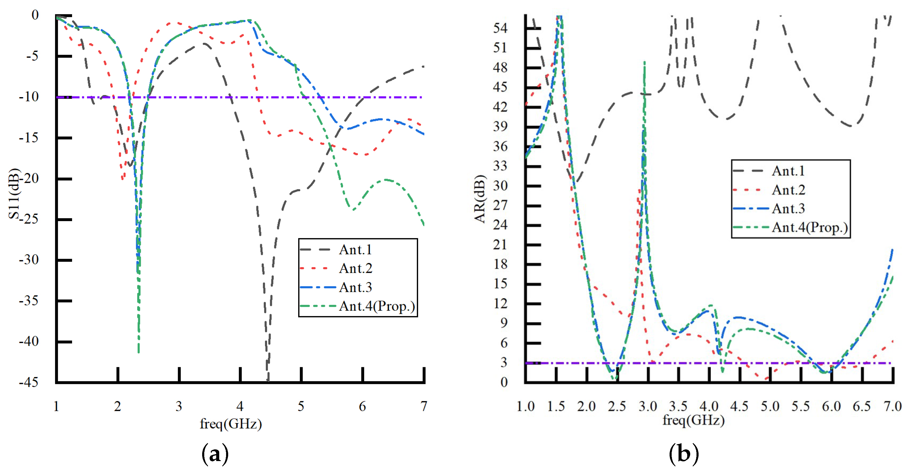
Figure 3.
Antenna equivalent circuit model diagram.
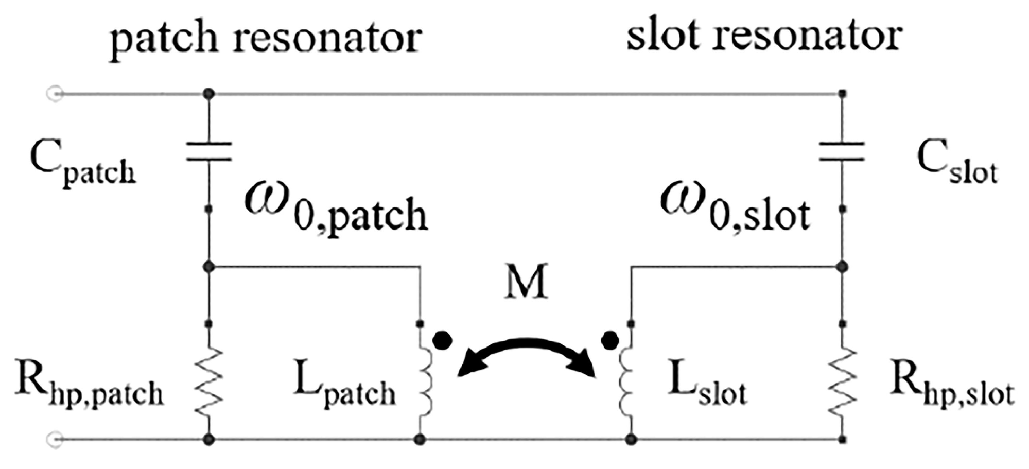
Figure 4.
Antenna surface current distribution. (a) 0 deg at 2.4 GHz; (b) 90 deg at 2.4 GHz; (c) 0 deg at 5.8 GHz; (d) 90 deg at 5.8 GHz.
Figure 4.
Antenna surface current distribution. (a) 0 deg at 2.4 GHz; (b) 90 deg at 2.4 GHz; (c) 0 deg at 5.8 GHz; (d) 90 deg at 5.8 GHz.

Figure 5.
Effect of parameter L2 on the bandwidth of antenna S11 (a) and 3-dB axial ratio (b).
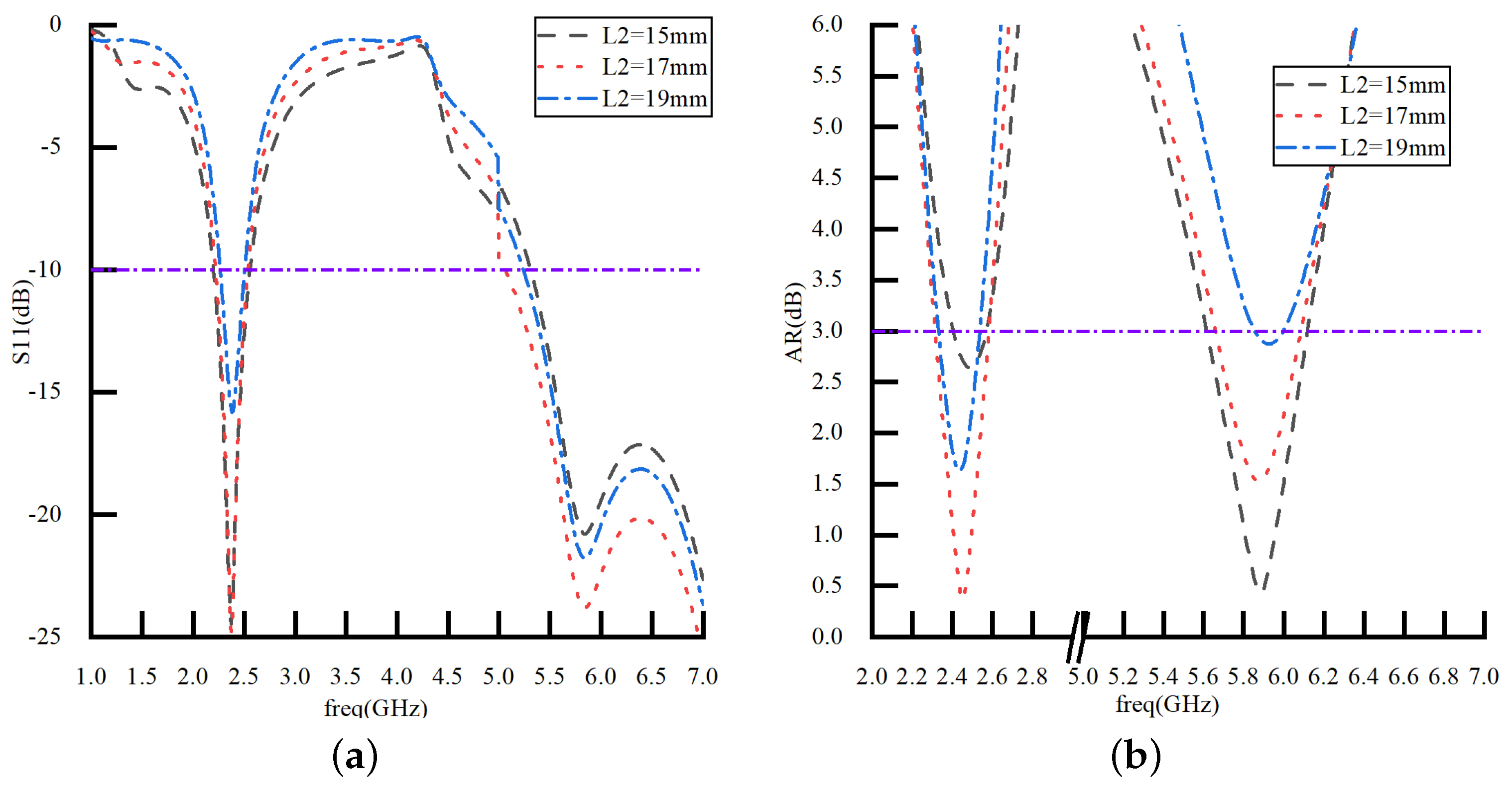
Figure 6.
Effect of parameter W2 on the bandwidth of antenna S11 (a) and 3-dB axial ratio (b).

Figure 7.
Effect of parameter L3 on the bandwidth of antenna S11 (a) and 3-dB axial ratio (b).
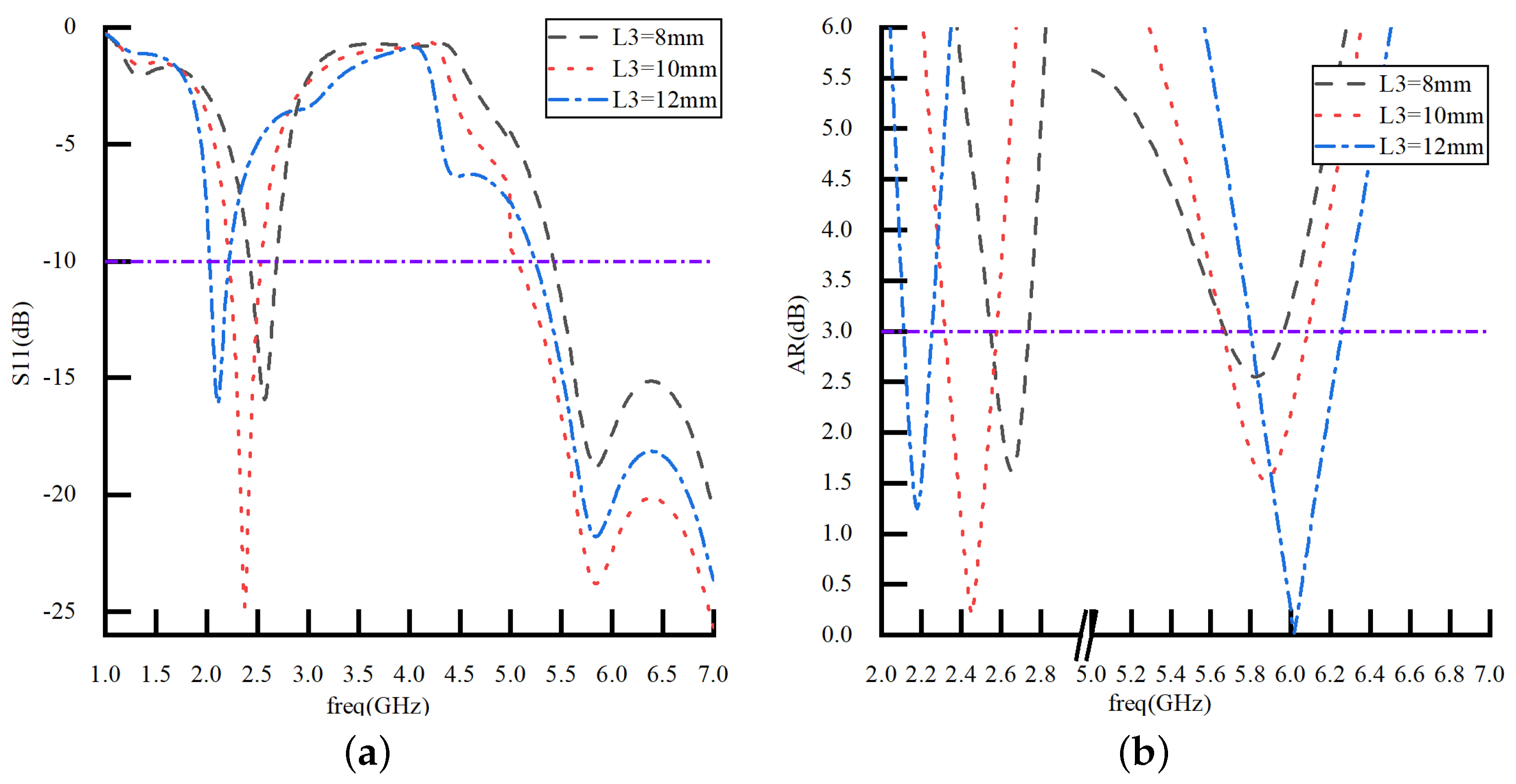
Figure 8.
Effect of parameter L4 on the bandwidth of antenna S11 (a) and 3-dB axial ratio (b).
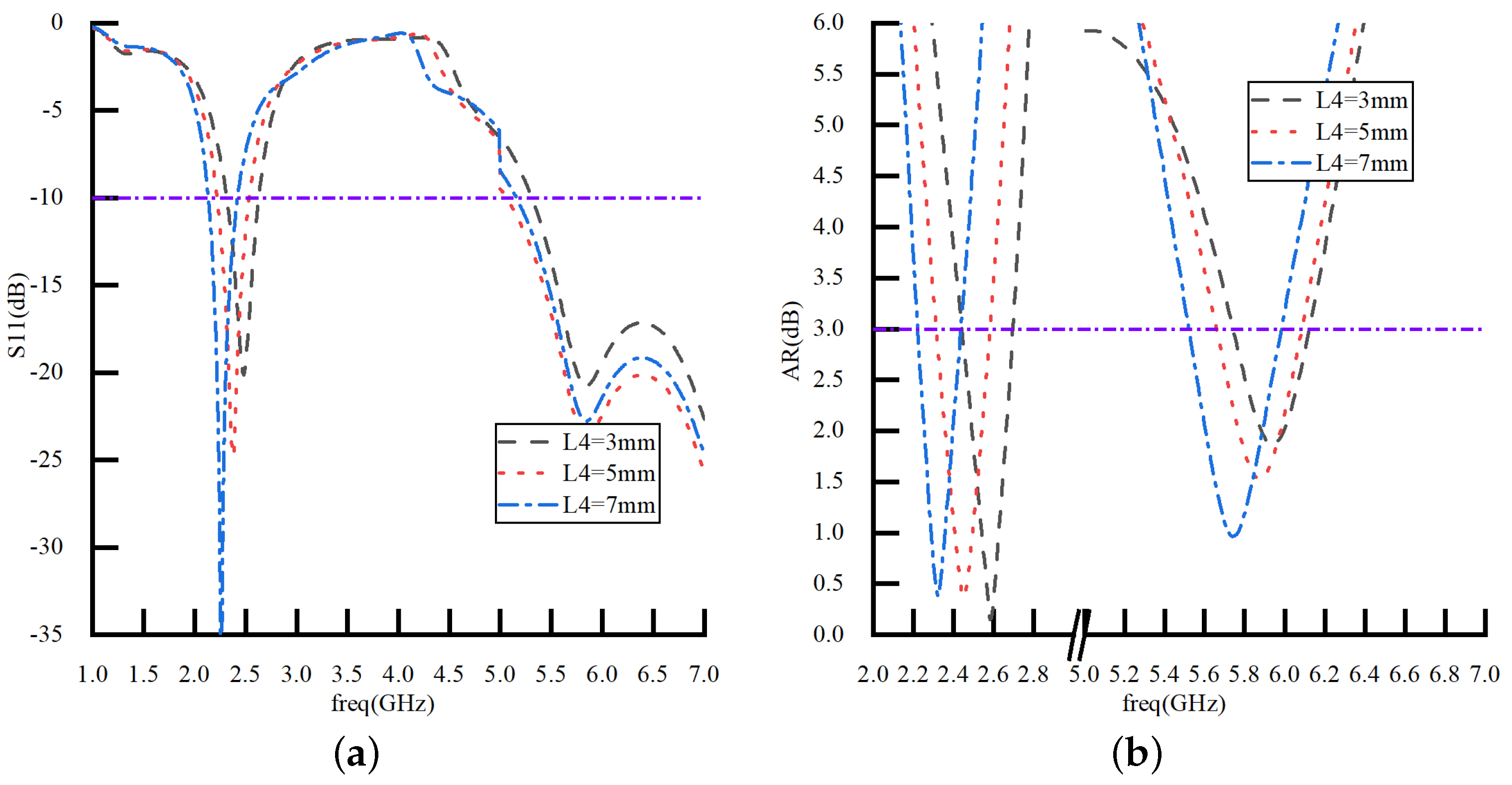
Figure 9.
Antenna pattern at 2.4 GHz (a) and gain frequency relationship diagram (b).
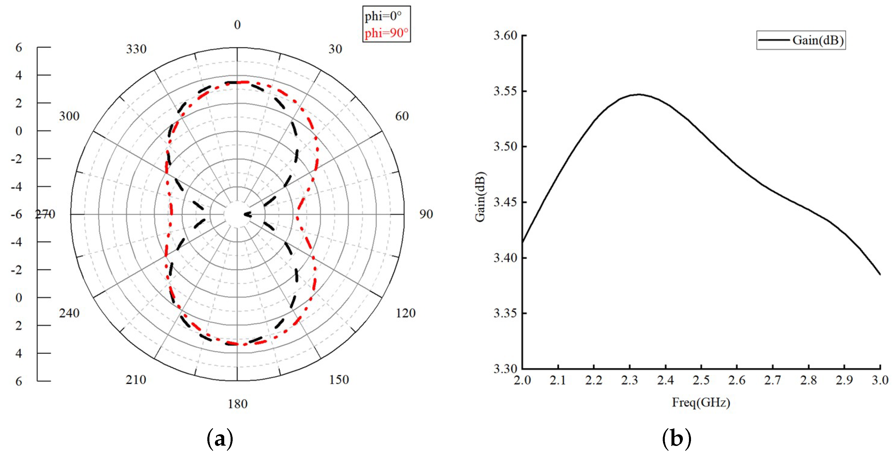
Figure 10.
Antenna pattern at 5.8 GHz (a) and gain frequency relationship diagram (b).
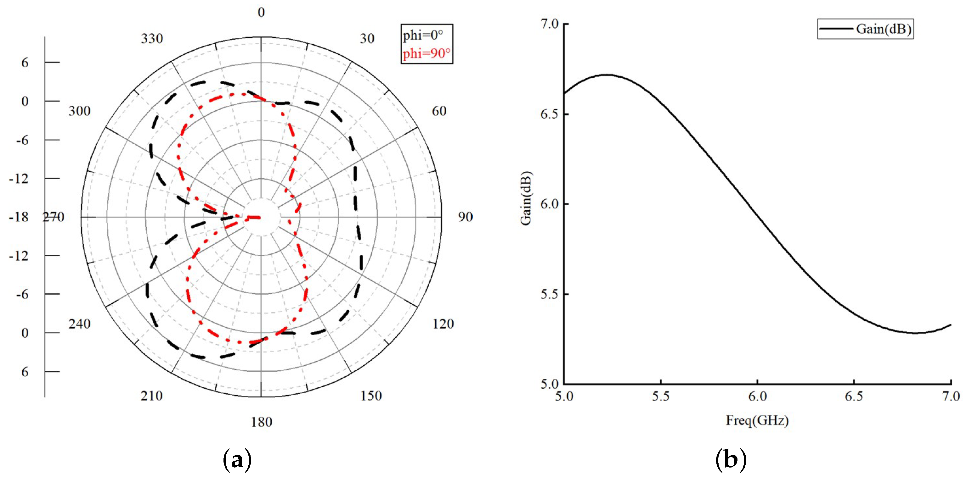
Figure 11.
Rectifier circuit layout.
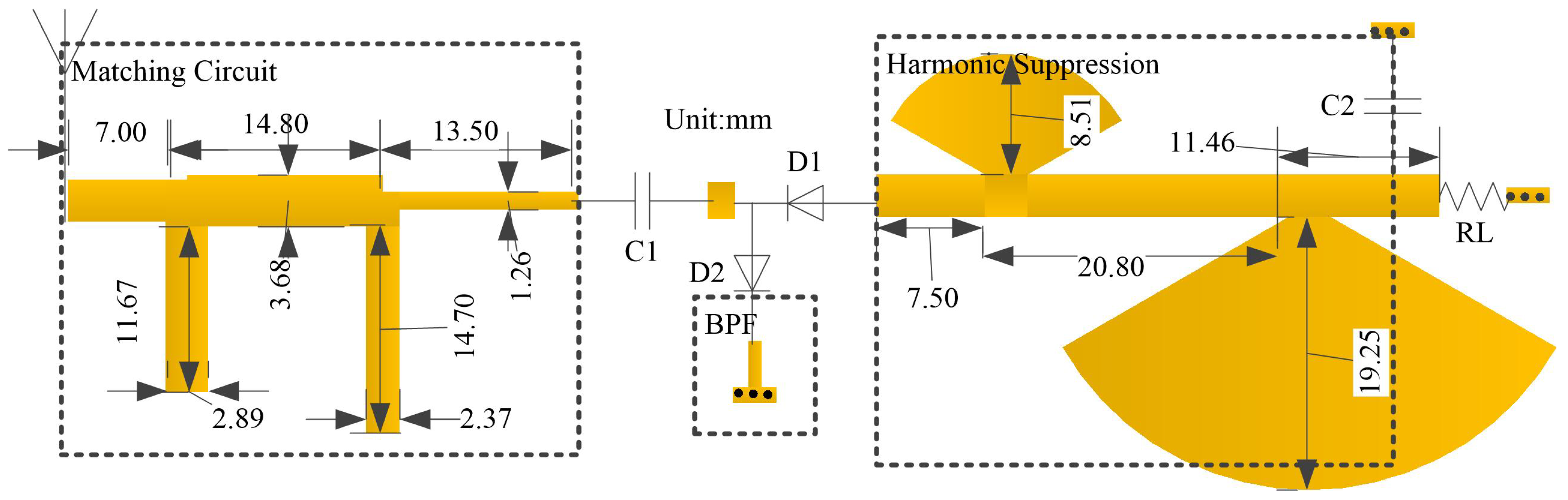
Figure 12.
Output low−pass filter S11 curve.
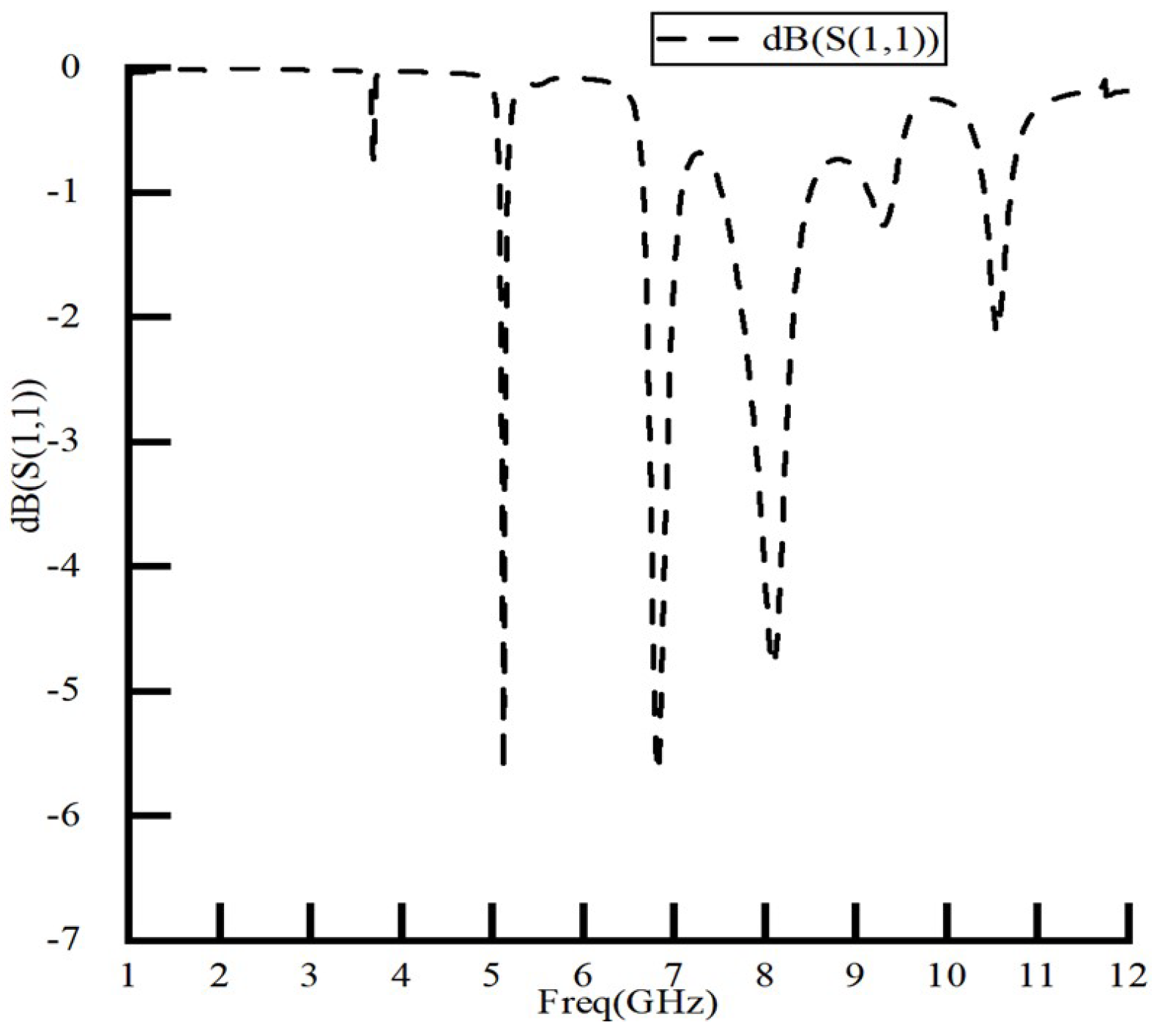
Figure 13.
Input impedance curve of rectifier circuit versus (a) frequency and (b) input power.

Figure 14.
Rectifier circuit S11 curve diagram.
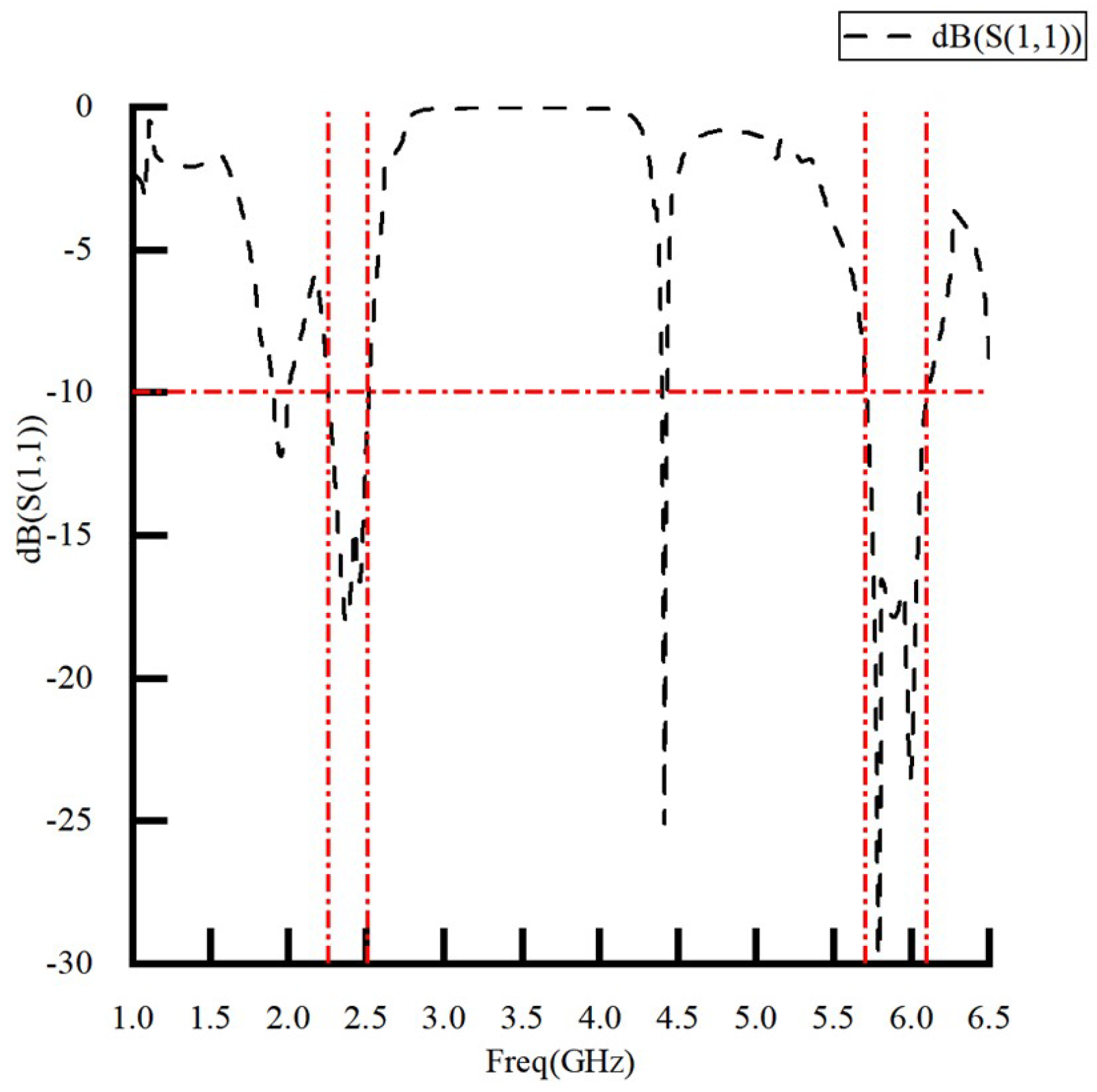
Figure 15.
Curve of rectification efficiency with input power.
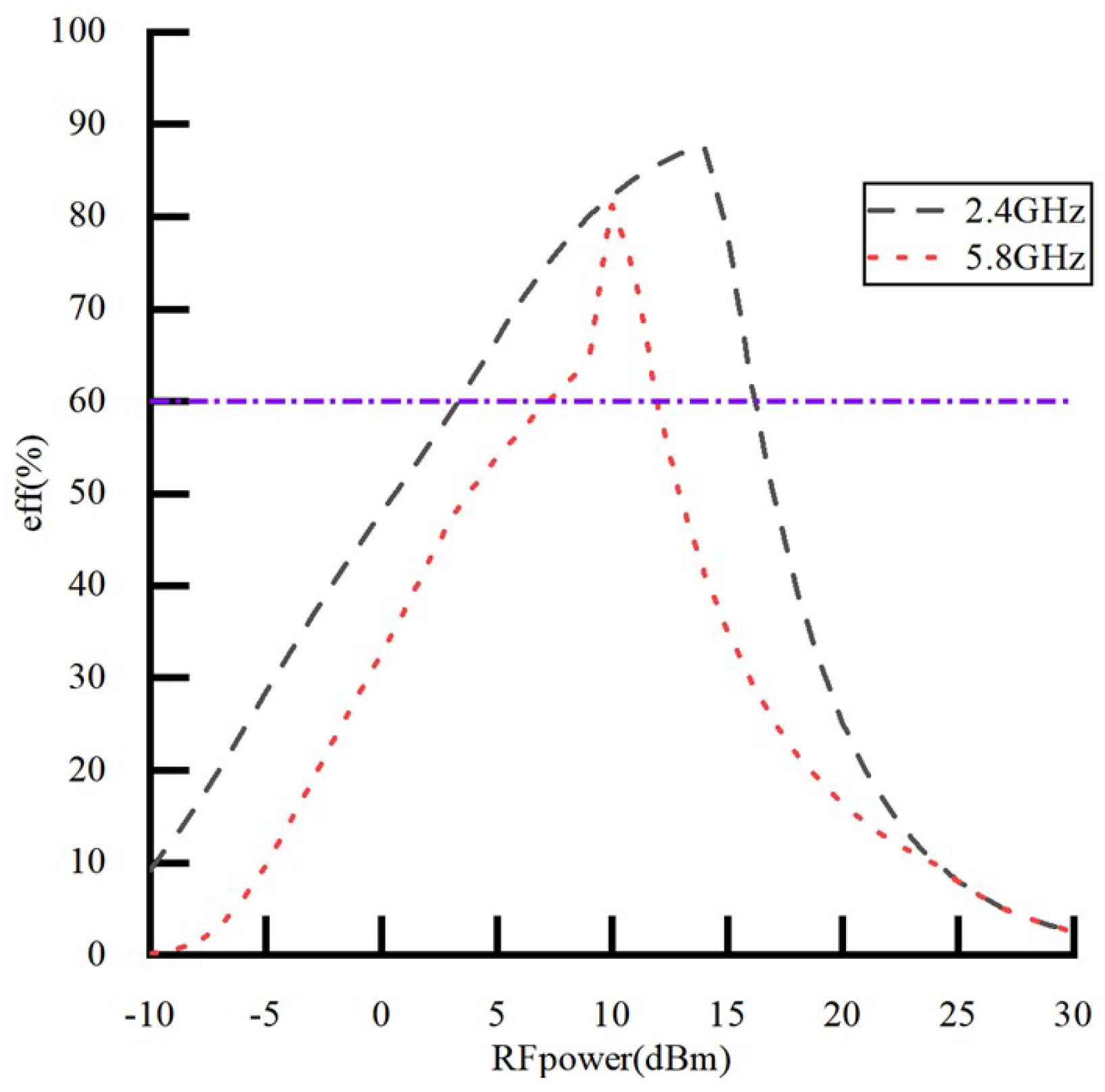
Figure 16.
Physical testing structure diagram.

Figure 17.
RF signal source output power. (a) 2.4 GHz; (b) 5.8 GHz.
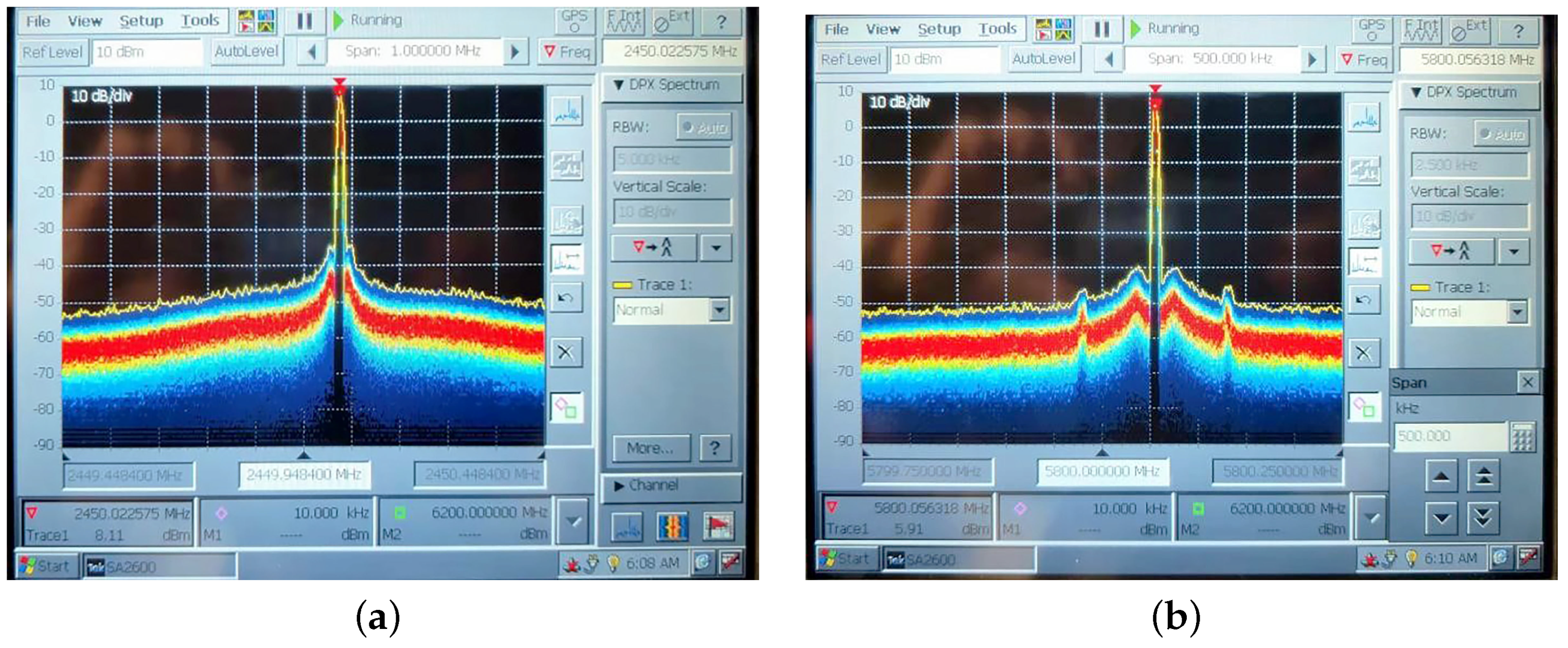
Figure 18.
Output DC voltage simulation and testing diagram.

Figure 19.
Results of the physical test. (a) 2.4 GHz; (b) 5.8 GHz.


Table 1.
Dimensions of the proposed antenna.
| Parameters | SX | SY | d0 | L4 | W | L1 | D |
| Unit(mm) | 45 | 45 | 5 | 5 | 10 | 13 | 6 |
| Parameters | d1 | d2 | L | W2 | L2 | L3 | W3 |
| Unit(mm) | 3 | 4 | 13 | 30 | 17 | 10 | 3 |
Table 2.
Comparison of simulation and physical test results.
| Input Frequency | Simulation DC(V)/Efficiency | Measurement DC(V)/Efficiency |
|---|---|---|
| 2.4 | 3.85/82.3% | 3.71/79.3% |
| 5.8 | 3.83/82% | 2.82/60.0% |
Disclaimer/Publisher’s Note: The statements, opinions and data contained in all publications are solely those of the individual author(s) and contributor(s) and not of MDPI and/or the editor(s). MDPI and/or the editor(s) disclaim responsibility for any injury to people or property resulting from any ideas, methods, instructions or products referred to in the content. |
© 2023 by the authors. Licensee MDPI, Basel, Switzerland. This article is an open access article distributed under the terms and conditions of the Creative Commons Attribution (CC BY) license (https://creativecommons.org/licenses/by/4.0/).
Share and Cite
MDPI and ACS Style
Deng, X.; Yang, P.; Chen, S.; Ren, W. Design of a 2.4 & 5.8 GHz Efficient Circularly Polarized Rectenna for Wireless Power Transfer Applications. Electronics 2023, 12, 2645. https://doi.org/10.3390/electronics12122645
AMA Style
Deng X, Yang P, Chen S, Ren W. Design of a 2.4 & 5.8 GHz Efficient Circularly Polarized Rectenna for Wireless Power Transfer Applications. Electronics. 2023; 12(12):2645. https://doi.org/10.3390/electronics12122645
Chicago/Turabian StyleDeng, Xizhou, Ping Yang, Shengtao Chen, and Wang Ren. 2023. "Design of a 2.4 & 5.8 GHz Efficient Circularly Polarized Rectenna for Wireless Power Transfer Applications" Electronics 12, no. 12: 2645. https://doi.org/10.3390/electronics12122645
Note that from the first issue of 2016, this journal uses article numbers instead of page numbers. See further details here.