Article

Graphene Multi-Frequency Broadband and Ultra-Broadband Terahertz Absorber Based on Surface Plasmon Resonance

1
Joint Laboratory for Extreme Conditions Matter Properties, Tianfu Institute of Research and Innovation, State Key Laboratory of Environmental Friendly Energy Materials, Key Laboratory of Manufacturing Process Testing Technology of Ministry of Education, Southwest University of Science and Technology, Mianyang 621010, China
2
State Key Laboratory of Electronic Thin Film and Integrated Devices, School of Electronic Science and Engineering, University of Electronic Science and Technology of China, Chengdu 610054, China
3
Department of Applied Physics, College of Science, Zhejiang University of Technology, Hangzhou 310023, China
4
School of Chemistry and Chemical Engineering, Jishou University, Jishou 416000, China
5
School of Automation, Hangzhou Dianzi University, Hangzhou 310018, China
6
Key Laboratory of Metallurgical Equipment and Control Technology of Ministry of Education, Wuhan University of Science and Technology, Wuhan 430081, China
7
School of Microelectronics and Control Engineering, Changzhou University, Changzhou 213164, China
8
College of Physics and Electronics, Central South University, Changsha 410083, China
*
Authors to whom correspondence should be addressed.
These authors contributed equally to this work.
Electronics 2023, 12(12), 2655; https://doi.org/10.3390/electronics12122655
Submission received: 9 May 2023 / Revised: 8 June 2023 / Accepted: 12 June 2023 / Published: 13 June 2023

Abstract

:
When surface plasmon resonance (SPR) occurs, the incident light is absorbed by the surface of the SPR structure, thus minimizing the intensity of the reflected light. Therefore, the SPR method is adopted in this paper to achieve perfect absorption of the absorbent. In this paper, we first propose a multi-frequency broadband absorber structure based on graphene SPR, which uses the continuous resonance of patterned graphene surface plasmon in the frequency spectrum to form a multi-frequency broadband absorption. In this simulation, a sandwich-stack structure was adopted, whereby the patterned graphene is situated on top of the SiO2 layer and the metal layer. The broad-band absorption bands of the absorber were obtained as 4.14–4.38 THz, 5.78–6.36 THz, and 7.87–8.66 THz through the analog simulation of finite-difference time-domain method (FDTD) solutions. Then, based on the multi-layer resonant unit structure, through the superposition and combination of absorbing units responding to different frequency bands, the perfect absorption of ultra-wideband is achieved. The data results illustrate that the total absorption bandwidth of the absorber is 2.26 THz, and the relative absorption bandwidth Bw is equal to 28.93%. The electric field in X-Y direction of the absorber in the perfect absorption band is analyzed, respectively, and the dynamic tunability of the absorber is studied. Finally, we studied whether the absorbing structure still has efficient absorption characteristics for the two polarization modes when the incident angle is changed from 0° to 70°. The structure model proposed has potential value for application in terahertz photoelectric detection, filtering, and electromagnetic shielding.

1. Introduction

At present, the perfect metamaterial absorber (PMA) appeals to researchers’ interest due to its high-efficiency ability to absorb electromagnetic waves, which can be applied in the fields of electromagnetic shielding, photoelectric sensing, and optical stealth [1,2,3,4,5]. Perfect absorbing devices are one of the important components in many practical applications, including selective thermal emitters, high-efficiency solar cells, photoelectric detection, and electromagnetic shielding [6,7,8,9,10,11]. Moreover, contrary to the limited absorbing characteristics of narrow-band absorbers, broadband absorbers have a wider range of applications in filtering, shielding, and other fields. For example, in 2016, Hu Dan et al. designed a circular metamaterial absorber through numerical simulation [12]. The absorber achieves broadband absorption up to more than 90% of the absorption width of 1.43 THz. In 2018, Lu Yuying et al. proposed a polarization-insensitive broadband terahertz metamaterial absorber [13]. The simulation results show that the absorption bandwidth covers the broadband frequency range of 0.22–0.33 THz, and the maximum absorption rate is 99.93% at 0.303 THz. The results show that it is feasible to design the broadband terahertz absorber by introducing a multi-scale metamaterial resonant structure. However, due to the fixed structure of such absorbers, the absorption band range cannot be changed [14,15]. Moreover, the complex structure increases the processing cost, and cannot greatly improve the bandwidth.
At present, the most direct way for many college students to realize broadband wave absorption is to use the broadband wave absorber formed by the combination of multiple resonance structures. For example, Yao Gang et al. established an absorber based on a multi-layer surface plasmon resonance (SPR) structure, providing a wide absorption bandwidth [16]. The absorber exhibits > 90% absorption over a broad frequency band of 0.55–3.12 THz. Next, in 2021, Xie Tong et al. proposed a terahertz absorber using fractal technology based on different geometric resonator structures of graphene [17]. This absorber achieves a broadband range of 1.26 THz (absorption > 80%). However, these methods of forming multi-resonance are more difficult to fabricate, with a large structure period, and sensitivity to polarized incident light [18,19,20]. In fact, the broadband-tunable metamaterial filter can also be realized by using a patterned resonator structure of graphene, and broadband absorption achieved by combining continuous resonance frequencies, so that the design can be miniaturized, the manufacturing can be simplified, and the absorption bandwidth can be effectively increased.
The broadband wave absorber has a good application prospect in electromagnetic stealth, shielding, and other aspects. Compared with SPR metal, the metamaterial absorber based on SPR has more excellent characteristics, such as a great mode limitation, and high inherent loss [21,22]. In this paper, we first design a multi-frequency broadband terahertz perfect absorber, based on the graphene SPR structure. The broadband absorption frequency bands of the absorber are 4.14–4.38 THz, 5.78–6.36 THz, and 7.87–8.66 THz, and the calculated total absorption bandwidth of the absorber is 1.51 THz. Finally, on the basis of multi-frequency broadband, an ultra-wideband graphene SPR terahertz absorber is designed, using the superposition and combination of absorbers. The absorber achieved the perfect absorption of ultra-wideband in the 7.0–9.5 THz band, with the total absorption bandwidth of 2.26 THz. The multifunctional wave absorber we designed possess the peculiarity of an adjustable absorption bandwidth and an insensitive angle. The proposed absorber has many potential applications in multi-functional devices, such as modulation and electromagnetic stealth.

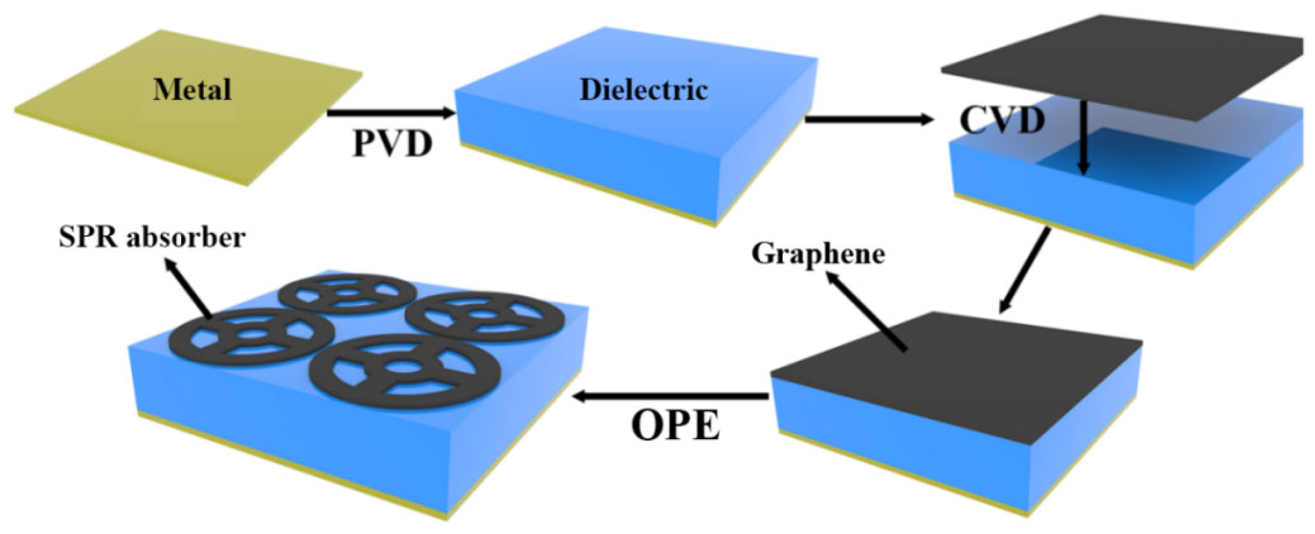
2. Theory and Method

The absorption principle of the metamaterial absorber can be explained using the Fabry–Pérot interference theory [23]. According to the Fabry–Pérot interference theory, the metamaterial absorber can be considered as a Fabry–Pérot interference resonant cavity, as shown in Figure 1. The graphene super surface at the roof of the structure is considered as a partial reflector, and the plate at the bottom is considered as a conduct to total reflection [24]. Due to the existence of the upper graphene structure and the lower metal layer, part of the terahertz wave transmitted from the surface of the graphene is reflected in the silicon dioxide absorption layer multiple times. This superposition of multiple reflections cancels out the direct reflection of the air from the graphene surface, achieving a high level of absorption. Therefore, all the reflection (R) coefficients of the incident light superimposed on the surface of the graphene structure can be expressed as [25,26]:
R = r 12 + t 12 t 21 r 23 e j 2 β + t 12 r 21 r 23 r 23 t 21 e j 4 β + t 12 r 21 r 23 r 23 r 23 t 21 e j 6 β + = r 12 ( t 12 t 21 r 12 r 21 ) e j 2 β 1 + r 21 e j 2 β = r 12 t 12 t 21 e j 2 β 1 + r 21 e j 2 β
where r 12 is the surface reflection coefficient, and t 12 is the transmission coefficient. The reflection coefficient of the bottom metal total reflection plate is r 23 = −1. β = ε r k 0 t 1 / c o s ( θ ) is the propagation phase, ε r is the relative dielectric constant, k0 is the wave vector, t 1 is the thickness of the SiO2 substrate, and θ is the incident angle. Therefore, in order to achieve perfect absorption, the reflection coefficient r 12 must be reduced to a maximum degree. The results of the wave absorber simulated in this paper will be verified using this theory. The absorption (A) of the wave absorber can be computed using the following formula [27,28,29,30]:
A ( ω ) = 1 T ( ω ) R ( ω ) = 1 S 21 ( ω ) 2 S 11 ( ω ) 2
In the formula, S 21 ( ω ) and S 11 ( ω ) are the transmitted and reflected amplitudes, respectively. T ( ω ) and R ( ω ) denote the transmission efficiency and reflection efficiency, respectively. Obviously, the absorption efficiency is maximal when T ( ω ) and R ( ω ) are small enough. The thickness of the metal layer is much greater than its skin depth in this design, which is enough to inhibit the transmission of all waves. Therefore, the A ( ω ) in this design can be derived from the following equation [31,32,33]:
A ( ω ) = 1 R ( ω )
That is to say, when it is close to zero, perfect absorption can be achieved. In order to calibrate the bandwidth level of the absorber, the relative absorption bandwidth Bw is calculated using Equation (4). Obviously, the relative absorption bandwidth can be expressed as the ratio of the total bandwidth to the center frequency. If the ratio is less than 1%, it is considered as narrowband. If it is within the range of 1–25%, it is considered as wideband. If it is greater than 25%, it is considered as ultra-wideband [34,35,36].
B w = 2 × ( f m a x f m i n ) ( f m a x + f m i n ) × 100 %
where f m a x and f m i n are the highest and lowest frequencies, respectively. In practical applications, devices are often constructed by applying gate voltage to regulate the Fermi level, and then affecting the conductivity of the graphene. The total conductivity of graphene can be expressed as σ g = σ i n t r a + σ i n t e r . σ i n t r a and σ i n t e r represent in-band and inter-band conductance, respectively. The conductivity of graphene can be considered as the following expression [37]:
σ i n t r a = i e 2 K B T π 2 ( ω + i τ 1 ) E F K B T + 2 l n e x p ( E F K B T ) + 1
σ i n t e r = i e 2 4 π 2 l n 2 E F ( ω + i τ 1 ) 2 E F + ( ω + i τ 1 )
Over here, e refers to the charge of the electron, KB refers to the Boltzmann constant, ħ = h/2π = 1.05 × 10⁻³⁴ J·s refers to the reduced Planck constant, T refers to the ambient temperature, w refers to the angular frequency of the incident light, and EF and τ refer to the Fermi energy and relaxation time of graphene, respectively. In the terahertz band EF >> ħw, the inter-band conductivity of graphene is negligible, and the conductivity of graphene is dependent on the in-band conductivity. Therefore, the total conductivity σ ( ω ) of graphene can be written as [38]:
σ ( ω ) = i e 2 | E F | π ħ 2 ( ω + i τ 1 )
According to Equation (7), the optoelectronic device of graphene can be regulated by adjusting the Fermi level and the relaxation time. This indicates that graphene can control its optical conductivity by changing the Fermi level. This continuous broadband-tunable photoconductivity of graphene simplifies the design of optoelectronic devices, and improves their flexibility of use [39].
Figure 2 shows the preparation process of the single-layer graphene SPR absorption structure. In the preparation process, the dielectric structure is grown on the metal base using physical vapor deposition (PVD). Then, the graphene layer is grown on the copper catalyst by chemical vapor deposition, and the isolation layer, transferred to silica using the wet method, is prepared by chemical vapor deposition (CVD) [40,41]. The single-layer patterned graphene structure is realized by electron beam lithography and oxygen plasmon etching (OPE). Finally, the photoresist is stripped, to obtain the final pattern of the graphene SPR absorption structure.

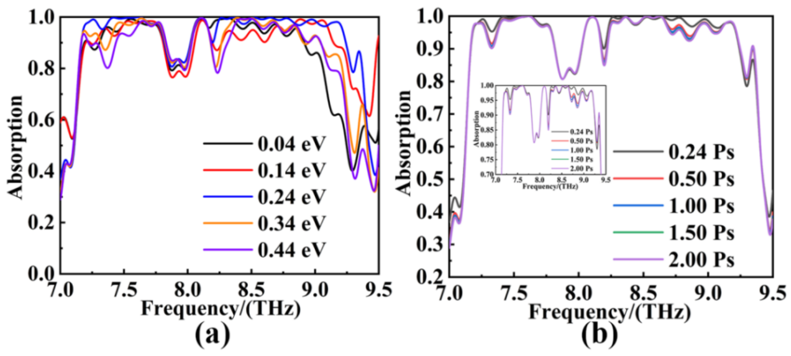
3. Design of the Multi-Frequency Broadband Model

In order to improve the absorption rate and the absorption bandwidth of the graphene to the terahertz wave, by designing a reasonable single-layer graphene structure, relatively strong continuous terahertz surface plasmons can be excited within a broadband range, so that perfect broadband absorption to the terahertz wave is achieved. Figure 3a,b show the structural diagram of the multi-frequency broadband graphene SPR absorber. A single layer of patterned graphene is situated on the roof of a silicon dioxide (SiO2) layer and a metal (Au) layer. The SiO2 refractive index n1 = 1.85, the relative dielectric constant εd = 3.4225, and the thickness T1 = 25 µm were selected. The bottom metal layer constitutes lossy Au with the conductivity σ = 5.25 × 10⁷ S/m and T2 = 0.5 µm, which can effectively prevent the transmission of terahertz wave. The overall period of the structure P = PX = PY = 25 µm. During the simulation, the optimal parameters of the patterned graphene layer were as follows: L1 = 5 µm, L2 = 8.5 µm, R1 = 9 µm, and R2 = 12 µm. The EF and τ of the patterned graphene layer were 0.15 eV and 0.15 Ps, respectively.
The absorption of the patterned graphene absorption structure in the 3.5–9.0 THz band is shown in Figure 4. It can be seen that the absorber realizes multi-frequency broadband absorption. In the frequency bands with the absorption rate greater than 80%, there are 4.14–4.38 THz (0.24 THz), 5.78–6.36 THz (0.48 THz), and 7.87–8.66 THz (0.79 THz). The center frequencies of the three broadband absorptions are 4.21 THz, 6.14 THz, and 8.35 THz, respectively. According to Equation (4), the relative absorption bandwidths Bw of the three absorption frequency bands are calculated to be 5.63%, 7.91%, and 9.55%, respectively. They are all within the range of 1–25%; i.e., multi-frequency broadband absorption is achieved [42], and the total absorption bandwidth is 1.51 THz. Notably, the absorber achieves more than 98% perfect absorption at 4.15–4.28 THz, 6.11–6.25 THz, and 8.07–8.66 THz, respectively. The theoretical curve is based on the calculation method of the reflection coefficient described in Formula 1, and the parameters simulated by the model are substituted to calculate the reflection efficiency in the frequency range of 3.5–9.0 THz, and then the absorption efficiency is calculated by Equation (3). The simulation results of FDTD Solutions have little deviation from the results verified by the Fabry–Pérot resonance theory. The reason for the deviation between the simulated absorption and the theoretical absorption is that the absorber is lossless. The absorber has a wide absorption bandwidth and a simple structure, and provides a new method for the broadband graphene absorber.
In order to understand the internal physical mechanism of the broadband absorption, the electric fields at different peaks were calculated, as shown in Figure 5a–d. It could be seen that the electric fields at 4.22 THz were mainly concentrated on the upper and lower parts of the ring, as well as on the inner side of the central square ring; the local electric fields at 6.21 THz were mainly concentrated on the upper and lower sides; and the electric fields at 8.07 THz and 8.45 THz were all concentrated on the outer side of the central square ring. The combined patterned graphene local absorption could result in stronger light absorption. It can be noted that the surface local electric field modes at 8.07 THz and 8.45 THz are similar, and this similar resonance mode achieves high-efficiency absorption at continuous frequencies, thus generating wider absorption [43,44,45]. In summary, high-efficiency absorption is the result of local surface plasmon resonance between the electromagnetic wave and the structure surface, and the absorbed resonance frequency is closely related to the structure of the resonant unit. It is shown that the method of expanding high-efficiency absorption bandwidth by the mutual fusion of adjacent resonance modes is effective.
In order to demonstrate the tunability of the multi-frequency broadband absorber, as shown in Figure 6a, the absorption curves of the absorber are studied when the EF is increasing from 0.10 eV to 0.30 eV. As the Fermi level increases from 0.10 eV to 0.30 eV, there is a slight blue shift in the resonance frequency from 4.08–4.32 THz on the left side, and the absorption efficiency remains unchanged. The absorption band at the middle 5.90–6.38 THz shows a weak blue shift, and the absorption peak can be increased from 85.68% to 99.53% with perfect absorption. The absorption band from 7.87–8.66 THz on the right remains unchanged, and the peak of the absorber can be adjusted from 65.54% to 99.65% perfect absorption. With the increase in the Fermi level of the graphene, the resonance frequency of SPR tends toward a high frequency. However, multi-frequency broadband absorption is caused by continuous terahertz surface plasmon resonance, and the mode of high-frequency resonance will change faster, while the mode of low-frequency resonance will change slower, so mode-splitting will occur at a high frequency. The absorption efficiency augments first, and then decreases, while the resonance of SPR reaches the maximum with the increase in the Fermi level. Nonetheless, when EF increases again, the interface becomes supersaturated, and the absorption decreases [46].
The absorption curve of the absorber when the refractive index n1 of SiO2 is increased from 1.79 to 1.91, is shown in Figure 6b. It can be seen from the figure that with the increase in the refractive index n1 of SiO2, the absorption efficiency and absorption bandwidth of the absorber are almost unchanged, and a certain red shift in the central resonance frequency of the multi-frequency broadband absorber is observed. The center frequency achieves modulation from 4.08–4.39 THz, 5.96–6.36 THz, and 8.07–8.64 THz. This is because the path phase φ P of the terahertz wave, when propagating in the dielectric layer, can be expressed as [47,48]:
φ P = 4 t ε r s i n 2 θ λ
where t and ε r are the thickness and dielectric constant of the dielectric lay, respectively. λ is the wavelength of the incident light. When the incident light is perpendicularly incident, φ P and θ can be regarded as fixed values. Thus, the center frequency is inversely proportional to the dielectric constant of the dielectric layer. When the refractive index n1 increases, the dielectric constant ε r increases, resulting in a red shift in the center frequency. In summary, the proposed multi-frequency broadband graphene SPR absorber has excellent modulation characteristics. The absorber can be applied to terahertz broadband attenuators, filters, or spatial modulators [49,50].
Figure 7a,b show the effect of the incident light angle from 0° to 70° on the absorption of the multi-frequency broadband absorber with TE and TM polarization. It can be clearly seen that the multi-frequency broadband absorber still has relatively stable absorption characteristics, along with the variation in the incident angle. Moreover, when the incident angle is 0°, the absorption spectra of TE and TM polarization are the same. Therefore, the absorber has the characteristic of symmetrical structure, and is not sensitive to the polarized incident angle. In the process of the small incident angle from 0 to 40, the wave absorber maintains excellent angular stability. This is because the surface structure of graphene has a certain function of focusing light beams, which can ensure the stability of the light source under a small angle incidence. In TE mode, when the angle exceeds 50°, the peak in the intermediate broadband decreases slightly, while the absorption peak intensities in the other frequency broadband remain basically unchanged. Obviously, the resonant absorption in the incident TM mode decreases much faster than that in the TE mode. This is because the tangential component of the electric field of the electromagnetic wave in the multi-frequency broadband absorber is changed in TM mode, while the tangential component in TE mode remains unchanged. In addition, the blue shift in resonance frequency can be observed in TE and TM modes at large incident angles, which is due to the parasitic resonance of the graphene surface. However, the broadband and high absorption levels remain constant even at large angles of incidence, with absorbance in both modes remaining above 60% at 4.08–4.32 THz, 5.90–6.38 THz, and 7.87–8.66 THz. This polarization insensitivity, and wide-angle broadband absorption, make it ideal for detection, sensing, and other optoelectronic applications in the terahertz region. Table 1 shows the performance comparison of the multi-frequency broadband absorber proposed in this chapter with other similar absorbers [51,52,53,54]. The results show that the absorbing device has more absorption bands, and is insensitive to the incidence angle of the incident electromagnetic wave.

4. Design of Ultra-Wideband Wave Absorbing Model

Figure 8a shows a three-dimensional array diagram of the ultra-wideband graphene terahertz absorber. On the basis of the multi-frequency broadband absorber, the optimized complementary model and absorber units with different resonance responses are combined, to achieve the perfect absorption of ultra-wideband, and the structure is absolutely symmetrical. The specific structures are a metal reflecting layer, a SiO2 layer, a graphene pattern layer, a SiO2 layer, and a complementary graphene layer, respectively, from bottom to top. On the basis of multi-frequency broadband, the SiO2 waveguide layer is added upward, with the refractive index n 2 = 1.95, and thickness T 4 = 5 μm. The structure of the top-layer patterned graphene is shown in Figure 7b. The optimal structural parameters are as follows: edge length L 1 = 2.5 μm, L 2 = 3.0 μm, and radius R = 6.5 μm. When the EF and the τ of the top-layer patterned graphene are 0.24 eV and 0.24 Ps, respectively, the optimal absorption in the frequency band of 7.0–9.5 THz is achieved. The structure period of the ultra-wideband absorber is P = 25 μm, and the total height is H = 35.501 μm.
The absorption spectra of the bilayer graphene absorber at 7.0–9.5 THz are shown in Figure 9. The calculation shows that the frequency band with the absorption efficiency greater than 80% is in the range of 7.12–9.38 THz, and the total absorption bandwidth is 2.26 THz. According to Equation (4), the relative absorption bandwidth Bw = 28.93% > 25% is calculated, and the high-efficiency absorption of ultra-wideband is achieved [55]. Moreover, the total absorption bandwidth of the absorber is 1.98 THz at an absorption efficiency exceeding 95% near-perfect absorption. After comparing the solid line obtained using the simulation with the dotted line calculated by the Fabry–Pérot theory, we can find that they are basically similar, but the simulation results are less effective than the theoretical results. This is because the influence of the inherent loss of materials is not considered in the theoretical calculation, and the electromagnetic parameters of the simulated materials are introduced into the software simulation, which has certain loss. Therefore, the theoretical calculation is better than the simulation results.
The proposed ultra-wideband absorber is mainly based on the multi-layer graphene structure SPR, to achieve perfect absorption. To explore the internal physical mechanism of perfect absorption, the electric field distributions of the graphene layer in the perfect absorption bands of 7.5 THz, 8.5 THz, and 9.0 THz were studied in this paper, as shown in Figure 10. As shown in Figure 10a–c, the local electric field of the top graphene structure is mainly distributed at the openings at the left and right ends of the sector, and with the increase in the incident electromagnetic frequency, the local electric field is gradually transferred to the upper and lower openings. The local electric field distributions of the central graphene structure, with frequency variation, are shown in Figure 10d–f. It can be found that the local electric field is firstly distributed inside the square ring when the electromagnetic wave frequency is 7.5 THz. Then, as the frequency of the electromagnetic wave increases to 8.5 THz, the local electric field diverges outward, and is distributed at the four corners of the square ring, and within the ring. When the electromagnetic wave frequency is 9.0 THz, the local electric field is tightened to the inner side of the square ring, and a more local perfect absorption is formed. Obviously, in the perfect absorption band, the natural frequencies of electromagnetic waves, and the patterned structure, are coupled with each other, resulting in surface plasma oscillation [56,57]. A local electric field is caused, and the ultra-wideband perfect absorption in the frequency band range is realized.
Since the EF of the graphene material can be controlled by changing the grid voltage V f , we investigated the tunability when the EF of the top-layer graphene is increased from 0.04 eV to 0.22 eV, as shown in Figure 11a. Here, as the ultra-wideband absorber in this paper adopts the double-layer patterned graphene structure, considering that the applied voltage of the central patterned graphene is relatively complex in the actual manufacturing process, the EF of the central patterned graphene is fixed. The EF and τ are 0.15 eV, and 0.15 Ps, respectively, as the parameters of the multi-frequency broadband absorber. Therefore, the change in the EF of the top-layer graphene can regulate the bandwidth of the absorber. The absorption bandwidth with the absorption efficiency higher than 80% is regulated within the range of 1.85–2.26 THz. In the process of increasing the Fermi level of graphene, the bandwidth increases first, and then decreases, reflecting the process of surface plasmon resonance generated by the absorber from unsaturated, to critical saturated and, finally, supersaturated. The relaxation time of graphene can be regulated by changing the carrier mobility in graphene through weakly doping the graphene structure [58]. For this reason, we studied the absorption curve when the τ of the graphene increased from 0.24 Ps to 2.00 Ps, as shown in Figure 11b. Obviously, with the increase in the τ of the top-layer graphene, the absorption bandwidth of the ultra-wide band absorber hardly changes. The relaxation time has little effect on it, but the absorption efficiency tends to decrease gradually. When the relaxation time τ = 0.24 Ps, the absorption is best. Therefore, in the actual application process, the efficiency of the ultra-wideband absorber can be changed by changing the graphene relaxation time without affecting the absorption bandwidth.
In actual application, the incident light angle will be changed, so the characteristics of the polarization angle, and the large angle incidence of the incident wave, have great research needs. In this paper, by changing the polarization of the incident light source in the simulation process using FDTD Solutions, we studied the absorption of the absorber under the TE and TM polarization when the incident angle increased from 0° to 70°, as shown in Figure 12a,b. Obviously, when the incident angles are all 0°, the absorption efficiency of TE and TM is the same, because the designed ultra-wideband perfect absorber has the characteristics of absolute symmetry of structure, and is not sensitive to incident light sources of different polarizations [59]. Besides, it can be seen that the bandwidth of the ultra-wideband hardly changes with the increase in the incident angle. The absorption spectra at both polarizations achieve greater than 80% good absorption in the range of 7.12–9.38 THz, with better absorption efficiency with increasing angle. When the angle of incidence is 70°, the near-perfect absorption of more than 90% is achieved in the absorption spectrum of 7.12–9.38 THz for the two polarization modes. The comparison of the ultra-wideband absorber proposed in this paper with other similar absorbers is shown in Table 2 below [60,61,62,63,64]. Obviously, the ultra-wideband absorber proposed has the characteristics of an ultra-wide absorption bandwidth, dynamic tunability, polarization independence, and large angle insensitivity, meaning the ultra-wideband absorber has more effects in practical applications.

5. Conclusions

To summarize, in this paper, based on the graphene SPR structure, two optimized tunable absorbers in the THz band are designed, which achieve perfect absorption in multi-frequency and ultra-wideband, respectively. The results are verified by the FDTD method calculation model, and Fabry–Pérot resonance theory. The multi-frequency broadband graphene terahertz wave absorber has a simple structure, and high-efficiency absorption, with wide multi-frequency, is realized in a 3.5–9.0 THz frequency band. The designed ultra-wideband graphene SPR terahertz absorber adopts a double-layer graphene SPR structure. Based on the multi-frequency broadband structure, the SiO2 waveguide layer, and the top-layer patterned graphene, were added. The combination of the two realizes the ultra-wideband absorption in the 7.0–9.5 THz frequency band. The designed absorber has the property of adjustable bandwidth, and is not sensitive to the polarization and incidence angle of the incident terahertz. Compared with similar wave absorbers, it has more excellent characteristics, and more plasticity. This paper will lay an important theoretical and technical foundation for the development of THz-absorbing devices, which can be widely used in the fields of THz filtering, electromagnetic shielding, and optical attenuation, and has important practical value.

Author Contributions

Z.C.: conceptualization, formal analysis, investigation, data curation, writing—original draft, writing—review & editing. P.C.: conceptualization, formal analysis, investigation, data curation, funding acquisition. Q.W.: conceptualization, formal analysis, investigation, data curation, funding acquisition. H.C.: conceptualization, formal analysis, investigation, data curation, funding acquisition. Y.T.: conceptualization, formal analysis, investigation, data curation, funding acquisition. Z.Y.: conceptualization, formal analysis, investigation, data curation. K.W.: conceptualization, formal analysis, investigation. G.L.: conceptualization, formal analysis, investigation. B.T.: conceptualization, formal analysis, investigation. Y.Y.: conceptualization, formal analysis, investigation. All authors have read and agreed to the published version of the manuscript.

Funding

The authors are grateful for the support from National Natural Science Foundation of China (No. 11604311, 12074151, 11704223); the fund by the Open Fund of Hubei Key Laboratory of Mechanical Transmission and Manufacturing Engineering at Wuhan University of Science and Technology (MTMEOF2021B02); the funded by the Open Fund of The Key Laboratory for Metallurgical Equipment and Control Technology of Ministry of Education in Wuhan University of Science and Technology (No. MECOF2022B01); the funded by the Opening Project of Key Laboratory of Microelectronic Devices & Integrated Technology, Institute of Microelectronics, Chinese Academy of Sciences; the Funded by the second batch of industry university cooperation collaborative education project in 2021 (202102153027).

Institutional Review Board Statement

Not applicable.

Informed Consent Statement

Not applicable.

Data Availability Statement

Publicly available datasets were analyzed in this study. These data can be found here: [https://www.lumerical.com/ (accessed on 1 January 2020)].

Conflicts of Interest

The authors declare no conflict of interest.

References

  1. Ye, Z.; Wu, P.; Wang, H.; Jiang, S.; Huang, M.; Lei, D.; Wu, F. Multimode tunable terahertz absorber based on a quarter graphene disk structure. Results Phys. 2023, 48, 106420. [Google Scholar] [CrossRef]
  2. Guo, Y.M.; Zhong, L.B.; Min, L.; Wang, J.Y.; Wu, Y.; Chen, K.L.; Wei, K.; Rao, C.H. Adaptive optics based on machine learning: A review. Opto-Electron. Adv. 2022, 5, 200082. [Google Scholar] [CrossRef]
  3. Ren, Y.; Zhou, T.; Jiang, C.; Tang, B. Thermally switching between perfect absorber and asymmetric transmission in vana-dium dioxide-assisted metamaterials. Opt. Express 2021, 29, 7666–7679. [Google Scholar] [CrossRef] [PubMed]
  4. Lai, R.; Shi, P.; Yi, Z.; Li, H.; Yi, Y. Triple-Band Surface Plasmon Resonance Metamaterial Absorber Based on Open-Ended Prohibited Sign Type Monolayer Graphene. Micromachines 2023, 14, 953. [Google Scholar] [CrossRef] [PubMed]
  5. Yao, L.; Koshelev, K.; Zhang, F.C.; Lin, H.; Lin, S.R.; Wu, J.Y.; Jia, B.H.; Kivshar, Y. Bound states in the continuum in ani-sotropic plasmonic metasurfaces. Nano Lett. 2020, 20, 6351–6356. [Google Scholar]
  6. Zheng, Y.; Yi, Z.; Liu, L.; Wu, X.W.; Liu, H.; Li, G.F.; Zeng, L.C.; Li, H.L.; Wu, P.H. Numerical simulation of efficient solar absorbers and thermal emitters based on multilayer nanodisk arrays. Appl. Therm. Eng. 2023, 230, 120841. [Google Scholar] [CrossRef]
  7. Wu, X.; Yin, C.; Zhang, M.; Xie, Y.; Hu, J.; Long, R.; Wu, X.; Wu, X. The Intercalation Cathode of MOFs-driven Vanadi-um-based Composite Embedded in N-doped Carbon for Aqueous Zinc ion Batteries. Chem. Eng. J. 2023, 452, 139573. [Google Scholar] [CrossRef]
  8. Meng, W.; Li, C.; Yao, M.; He, Z.; Wu, X.; Jiang, Z.; Dai, L.; Wang, L. Synthesis and electrochemical performance of Li1+xTi2−xFex(PO4)3/C anode for aqueous lithium ion battery. Adv. Powder Technol. 2020, 31, 1359–1364. [Google Scholar] [CrossRef]
  9. Liang, S.; Xu, F.; Yang, H.; Cheng, S.; Yang, W.; Yi, Z.; Song, Q.; Wu, P.; Chen, J.; Tang, C. Ultra long infrared metamaterial absorber with high absorption and broad band based on nano cross surrounding. Opt. Laser Technol. 2023, 158, 108789. [Google Scholar] [CrossRef]
  10. Zheng, Z.P.; Zhao, W.C.; Yi, Z.; Bian, L.; Yang, H.; Cheng, S.B.; Li, H.L.; Li, G.F.; Zeng, L.C.; Li, H.; et al. Active thermally tunable and highly sensitive terahertz smart windows based on the combination of a metamaterial and phase change material. Dalton Trans. 2023. [Google Scholar] [CrossRef]
  11. Cai, Y.P.; Huang, Y.; Zhu, K.Y. Toroidal Dipole Excitation in Metamaterial Perfect Absorber Consisting of Dielectric Nano-disks Quadrumer Clusters and Spacer on Metal Substrate. Photonics 2022, 9, 462. [Google Scholar] [CrossRef]
  12. Hu, D.; Wang, H.Y.; Tang, Z.J.; Zhang, X.Y. Investigation of a broadband refractory metal metamaterial absorber at terahertz frequencies. Appl. Opt. 2016, 55, 5257–5262. [Google Scholar] [CrossRef]
  13. Lu, Y.Y.; Li, J.N.; Zhang, S.H.; Sun, J.H.; Yao, J.Q. Polarization-insensitive broadband terahertz metamaterial absorber based on hybrid structures. Appl. Opt. 2018, 57, 6269–6275. [Google Scholar] [CrossRef] [PubMed]
  14. Wu, F.Y.; Shi, P.C.; Yi, Z.; Li, H.L.; Yi, Y.G. Ultra-Broadband Solar Absorber and High-Efficiency Thermal Emitter from UV to Mid-Infrared Spectrum. Micromachines 2023, 14, 985. [Google Scholar] [CrossRef] [PubMed]
  15. Qi, H.; Tang, B. An active tunable terahertz functional metamaterial based on hybrid-graphene vanadium dioxide. Phys. Chem. Chem. Phys. 2023, 25, 7825–7831. [Google Scholar] [CrossRef] [PubMed]
  16. Yao, G.; Ling, F.; Yue, J.; Luo, C.Y.; Ji, J.; Yao, J.Q. Dual-band tunable perfect metamaterial absorber in the THz range. Opt. Express 2016, 24, 1518–1527. [Google Scholar] [CrossRef]
  17. Xie, T.; Chen, D.B.; Yang, H.P. Tunable Broadband Terahertz Waveband Absorbers Based on Fractal Technology of Gra-phene Metamaterial. Nanomaterials 2021, 11, 269. [Google Scholar] [CrossRef]
  18. Li, W.; Ma, J.; Zhang, H.; Cheng, S.; Yang, W.; Yi, Z.; Yang, H.; Zhang, J.; Wu, X.; Wu, P. Tunable broadband absorber based on a layered resonant structure with a Dirac semimetal. Phys. Chem. Chem. Phys. 2023, 25, 8489–8496. [Google Scholar] [CrossRef]
  19. Wu, X.; Li, Y.; Xiang, Y.; Liu, Z.; He, Z.; Wu, X.; Li, Y.; Xiong, L.; Li, C.; Chen, J. The electrochemical performance of aqueous rechargeable battery of Zn/Na0.44MnO2 based on hybrid electrolyte. J. Power Sources 2016, 336, 35–39. [Google Scholar] [CrossRef]
  20. Li, Y.; Yang, S.; Du, H.; Liu, Y.; Wu, X.; Yin, C.; Wang, D.; Wu, X.; He, Z.; Wu, X. A stable fluoride-based interphase for a long cycle Zn metal anode in an aqueous zinc ion battery. J. Mater. Chem. A 2022, 10, 14399–14410. [Google Scholar] [CrossRef]
  21. Ren, Y.; Tang, B. Switchable Multi-Functional VO2-Integrated Metamaterial Devices in the Terahertz Region. J. Light Technol. 2021, 39, 5864–5868. [Google Scholar] [CrossRef]
  22. Wang, Z.; Liu, Y.; Li, L.; Gao, S.; Zhu, D.; Yu, X.; Cheng, S.; Zheng, D.; Xiong, Y. An investigation of the effects of ZnO inverse opal pore size in the composite of ZnO nanorods/ZnO inverse opal on the performance of quantum dot-sensitized solar cells. Dalton Trans. 2023, 52, 81–89. [Google Scholar] [CrossRef]
  23. Tang, B.; Guo, Z.; Jin, G. Polarization-controlled and symmetry-dependent multiple plasmon-induced transparency in graphene-based metasurfaces. Opt. Express 2022, 30, 35554–35566. [Google Scholar] [CrossRef]
  24. Li, W.; Yi, Y.; Yang, H.; Cheng, S.; Yang, W.; Zhang, H.; Yi, Z.; Yi, Y.; Li, H. Active tunable terahertz bandwidth absorber based on single layer graphene. Commun. Theor. Phys. 2023, 75, 045503. [Google Scholar] [CrossRef]
  25. Jia, Z.; Huang, L.; Su, J.; Tang, B. Tunable Electromagnetically Induced Transparency-Like in Graphene metasurfaces and its Application as a Refractive Index Sensor. J. Light Technol. 2021, 39, 1544–1549. [Google Scholar] [CrossRef]
  26. Shangguan, Q.; Chen, Z.; Yang, H.; Cheng, S.; Yang, W.; Yi, Z.; Wu, X.; Wang, S.; Yi, Y.; Wu, P. Design of Ultra-Narrow Band Graphene Refractive Index Sensor. Sensors 2022, 22, 6483. [Google Scholar] [CrossRef] [PubMed]
  27. Shangguan, Q.; Zhao, Y.; Song, Z.; Wang, J.; Yang, H.; Chen, J.; Liu, C.; Cheng, S.; Yang, W.; Yi, Z. High sensitivity active adjustable graphene absorber for refractive index sensing applications. Diam. Relat. Mater. 2022, 128, 109273. [Google Scholar] [CrossRef]
  28. Wu, X.; Li, Y.; Li, C.; He, Z.; Xiang, Y.; Xiong, L.; Chen, D.; Yu, Y.; Sun, K.; He, Z.; et al. The electrochemical performance improvement of LiMn2O4/Zn based on zinc foil as the current collector and thiourea as an electrolyte additive. J. Power Sources 2015, 300, 453–459. [Google Scholar] [CrossRef]
  29. Wu, X.; Li, Y.; Xiang, Y.; Liu, Z.; He, Z.; Wu, X.; Li, Y.; Xiong, L.; Li, C.; Chen, J. Mixed-valence cobalt oxides bifunctional electrocatalyst with rich oxygen vacancies for aqueous metal-air batteries. Chem. Eng. J. 2023, 453, 139831. [Google Scholar] [CrossRef]
  30. Tang, F.; Wu, X.; Shen, Y.; Xiang, Y.; Wu, X.; Xiong, L.; Wu, X. The intercalation cathode materials of heterostructure MnS/MnO with dual ions defect embedded in N-doped carbon fibers for aqueous zinc ion batteries. Energy Storage Mater. 2022, 52, 180–188. [Google Scholar] [CrossRef]
  31. Liu, Y.; Wang, Z.; Li, L.; Gao, S.; Zheng, D.; Yu, X.; Wu, Q.; Yang, Q.; Zhu, D.; Yang, W.; et al. Highly efficient quan-tum-dot-sensitized solar cells with composite semiconductor of ZnO nanorod and oxide inverse opal in photoanode. Elec-trochim. Acta 2022, 412, 140145. [Google Scholar] [CrossRef]
  32. Zhang, Y.; Yi, Y.; Li, W.; Liang, S.; Ma, J.; Cheng, S.; Yang, W.; Yi, Y. High Absorptivity and Ultra-Wideband Solar Absorber Based on Ti-Al2O3 Cross Elliptical Disk Arrays. Coatings 2023, 13, 531. [Google Scholar] [CrossRef]
  33. Zhu, L.; Hu, R.; Xiang, Y.; Yang, X.; Chen, Z.; Xiong, L.; Wu, X.; He, Z.; Lei, W. Enhanced performance of Li-S battery by constructing inner conductive network and outer adsorption layer sulfur-carbon composite. Int. J. Energy Res. 2020, 45, 6002–6014. [Google Scholar] [CrossRef]
  34. Tang, B.; Li, Z.; Palacios, E.; Liu, Z.; Butun, S.; Aydin, K. Chiral-Selective Plasmonic Metasurface Absorbers Operating at Visible Frequencies. IEEE Photon- Technol. Lett. 2017, 29, 295–298. [Google Scholar] [CrossRef]
  35. Li, C.; Shi, X.; Liang, S.; Ma, X.; Han, M.; Wu, X.; Zhou, J. Spatially homogeneous copper foam as surface dendrite-free host for zinc metal anode. Chem. Eng. J. 2020, 379, 122248. [Google Scholar] [CrossRef]
  36. Zhu, W.; Yi, Y.; Yi, Z.; Bian, L.; Yang, H.; Zhang, J.; Yu, Y.; Liu, C.; Li, G.; Wu, X. High confidence plasmonic sensor based on photonic crystal fibers with a U-shaped detection channel. Phys. Chem. Chem. Phys. 2023, 25, 8583–8591. [Google Scholar] [CrossRef] [PubMed]
  37. Shangguan, Q.; Chen, H.; Yang, H.; Liang, S.; Zhang, Y.; Cheng, S.; Yang, W.; Yi, Z.; Luo, Y.; Wu, P. A “belfry-typed” narrow-band tunable perfect absorber based on graphene and the application potential research. Diam. Relat. Mater. 2022, 125, 108973. [Google Scholar] [CrossRef]
  38. Chen, H.; Chen, Z.H.; Yang, H.; Wen, L.H.; Yi, Z.; Zhou, Z.G.; Dai, B.; Zhang, J.G.; Wu, X.W.; Wu, P.H. Multi-mode surface plasmon resonance absorber based on dart-type single-layer graphene. RSC Adv. 2022, 12, 7821–7829. [Google Scholar] [CrossRef]
  39. Tang, B.; Ren, Y. Tunable and switchable multi-functional terahertz metamaterials based on a hybrid vanadium dioxide–graphene integrated configuration. Phys. Chem. Chem. Phys. 2022, 24, 8408–8414. [Google Scholar] [CrossRef]
  40. Shan, L.; Zhou, J.; Zhang, W.; Xia, C.; Guo, S.; Ma, X.; Fang, G.; Wu, X.; Liang, S. Highly Reversible Phase Transition Endows V6O13 with Enhanced Performance as Aqueous Zinc-Ion Battery Cathode. Energy Technol. 2019, 7, 57. [Google Scholar] [CrossRef]
  41. Li, J.; Liu, G.; Liu, B.; Min, Z.; Qian, D.; Jiang, J.; Li, J. An extremely facile route to Co2P encased in N,P-codoped carbon layers: Highly efficient bifunctional electrocatalysts for ORR and OER. Int. J. Hydrogen Energy 2018, 43, 77. [Google Scholar] [CrossRef]
  42. Wang, D.; Yi, Z.; Ma, G.; Dai, B.; Yang, J.; Zhang, J.; Yu, Y.; Liu, C.; Wu, X.; Bian, Q. Two-channel photonic crystal fiber based on surface plasmon resonance for magnetic field and temperature dual-parameter sensing. Phys. Chem. Chem. Phys. 2022, 24, 21233–21241. [Google Scholar] [CrossRef] [PubMed]
  43. Wu, X.; Tan, C.; He, C.; Zhao, T.; Wu, X.; Ma, Z.; Wang, H.; Cai, Y.; Wu, Q.; Li, Q. Strategy for boosting Co-Nx content for oxygen reduction reaction in aqueous metal-air batteries. J. Power Sources 2021, 520, 230891. [Google Scholar] [CrossRef]
  44. Zheng, Z.; Luo, Y.; Yang, H.; Yi, Z.; Zhang, J.; Song, Q.; Yang, W.; Liu, C.; Wu, X.; Wu, P. Thermal tuning of terahertz metamaterial properties based on phase change material vanadium dioxide. Phys. Chem. Chem. Phys. 2022, 24, 8846–8853. [Google Scholar] [CrossRef]
  45. Zhu, Y.; Tang, B.; Yang, N.; Lang, X.; Su, J.; Li, Z. Tunable wide-angle perfect absorber based on black phospho-rous-dielectric-metallic hybrid architecture. Phys. E 2021, 126, 114449. [Google Scholar] [CrossRef]
  46. Zheng, Z.; Zheng, Y.; Luo, Y.; Yi, Z.; Zhang, J.; Liu, Z.; Yang, W.; Yu, Y.; Wu, X.; Wu, P. Switchable terahertz device com-bining ultra-wideband absorption and ultra-wideband complete reflection. Phys. Chem. Chem. Phys. 2022, 24, 2527–2533. [Google Scholar] [CrossRef] [PubMed]
  47. Wang, X.; Lin, J.; Yan, Z.; Yi, Z.; Yu, J.; Zhang, W.; Qin, F.; Wu, X.; Zhang, J.; Wu, P. Tunable high-sensitivity sensing detector based on Bulk Dirac semimetal. RSC Adv. 2022, 12, 32583–32591. [Google Scholar] [CrossRef]
  48. Wu, X.; Zheng, Y.; Luo, Y.; Zhang, J.; Yi, Z.; Wu, X.; Cheng, S.; Yang, W.; Yu, Y.; Wu, P. A four-band and polariza-tion-independent BDS-based tunable absorber with high refractive index sensitivity. Phys. Chem. Chem. Phys. 2021, 23, 26864–26873. [Google Scholar] [CrossRef]
  49. Tang, B.; Yang, N.; Huang, L.; Su, J.; Jiang, C. Tunable anisotropic perfect enhancement absorption in black phospho-rus-based metasurfaces. IEEE Photonics J. 2020, 12, 4500209. [Google Scholar] [CrossRef]
  50. Zhao, F.; Lin, J.; Lei, Z.; Yi, Z.; Qin, F.; Zhang, J.; Liu, L.; Wu, X.; Yang, W.; Wu, P. Realization of 18.97% theoretical efficiency of 0.9 µm Thick c-Si/ZnO Heterojunction Ultrathin-film Solar Cells via Surface Plasmon Resonance Enhancement. Phys. Chem. Chem. Phys. 2022, 24, 4871–4880. [Google Scholar] [CrossRef]
  51. Cai, Y.; Xu, K.-D. Tunable broadband terahertz absorber based on multilayer graphene-sandwiched plasmonic structure. Opt. Express 2018, 26, 31693–31705. [Google Scholar] [CrossRef]
  52. Qi, L.; Liu, C.; Shah, S.M.A. A broad dual-band switchable graphene-based terahertz metamaterial absorber. Carbon 2019, 153, 179–188. [Google Scholar] [CrossRef]
  53. Hu, D.; Meng, T.H.; Wang, H.Y.; Fu, M.X. Actively tunable dual-broadband graphene-based terahertz metamaterial ab-sorber. Chin. Phys. B 2021, 30, 126101. [Google Scholar] [CrossRef]
  54. Wu, D.; Wang, M.; Feng, H.; Xu, Z.X.; Liu, Y.P.; Xia, F.; Zhang, K.; Kong, W.J.; Dong, L.F.; Yun, M.J. Independently tunable perfect absorber based on the plasmonic properties in double-layer graphene. Carbon 2019, 155, 618–623. [Google Scholar] [CrossRef]
  55. Zhou, F.; Qin, F.; Yi, Z.; Yao, W.; Liu, Z.; Wu, X.; Wu, P. Ultra-wideband and wide-angle perfect solar energy absorber based on Ti nanorings surface plasmon resonance. Phys. Chem. Chem. Phys. 2021, 23, 17041–17048. [Google Scholar] [CrossRef]
  56. Tang, B.; Jia, Z.; Huang, L.; Su, J.; Jiang, C. Polarization-Controlled Dynamically Tunable Electromagnetically Induced Transparency-Like Effect Based on Graphene Metasurfaces. IEEE J. Sel. Top. Quantum Electron. 2020, 27, 4700406. [Google Scholar] [CrossRef]
  57. Zhu, Y.; Tang, B.; Jiang, C. Tunable broadband bandwidth anisotropic absorber based on multi-layer black phosphorus ribbons. Appl. Phys. Express 2019, 12, 032009. [Google Scholar] [CrossRef]
  58. Li, Y.H.; Xu, Y.P.; Jiang, J.B.; Ren, L.R.; Cheng, S.B.; Yang, W.X.; Ma, C.J.; Zhou, X.W.; Wang, Z.Y.; Chen, Z.Y. Quadruple plasmon-induced transparency and tunable multi-frequency switch in monolayer graphene terahertz metamaterial. J. Phys. D Appl. Phys. 2022, 55, 155101. [Google Scholar] [CrossRef]
  59. Zhang, Y.X.; Pu, M.B.; Jin, J.J.; Lu, X.J.; Guo, Y.H.; Cai, J.X.; Zhang, F.; Ha, Y.L.; He, Q.; Xu, M.F.; et al. Crosstalk-free achromatic full Stokes imaging polarimetry metasurface enabled by polarization-dependent phase optimization. Opto-Electron. Adv. 2022, 5, 220058. [Google Scholar] [CrossRef]
  60. Mou, N.; Sun, S.; Dong, H.; Dong, S.H.; He, Q.; Zhou, L.; Zhang, L. Hybridization-induced broadband terahertz wave ab-sorption with graphene metasurfaces. Opt. Express 2018, 26, 11728–11736. [Google Scholar] [CrossRef] [Green Version]
  61. Fu, P.; Liu, F.; Ren, G.J.; Fei, S.; Dong, L.; Jian, Q.Y. A broadband metamaterial absorber based on multi-layer graphene in the terahertz region. Opt. Commun. 2018, 417, 62–66. [Google Scholar] [CrossRef]
  62. Wu, S.; Li, J.-S. Hollow-petal graphene metasurface for broadband tunable THz absorption. Appl. Opt. 2019, 58, 3023–3028. [Google Scholar] [CrossRef] [PubMed]
  63. Biabanifard, S.; Biabanifard, M.; Asgari, S.; Asadi, S.; Yagoub, M.C.E. Tunable ultra-wideband terahertz absorber based on graphene disks and ribbons. Opt. Commun. 2018, 427, 418–425. [Google Scholar] [CrossRef]
  64. Huang, M.; Wei, K.; Wu, P.; Xu, D.; Xu, Y. Terahertz Broadband Absorber Based on a Combined Circular Disc Structure. Micromachines 2021, 12, 1290. [Google Scholar] [CrossRef] [PubMed]
Figure 1. Theoretical diagram of the Fabry–Pérot resonance of the single-layer graphene absorber.
Electronics 12 02655 g001
Figure 2. Preparation process of the monolayer pattern graphene SPR absorption structure.
Electronics 12 02655 g002
Figure 3. (a) Three-dimensional perspective view of a multi-frequency broadband graphene SPR absorber array. (b) Top view of the absorber.
Electronics 12 02655 g003
Figure 4. Absorption spectrum of the multi-frequency broadband graphene SPR absorber in the range of 3.5–9.0 THz. (a) Total spectral absorption chart. (bd) These show the absorption spectra at 3.50–4.50 THz, 5.75–6.50 THz, and 7.50–9.00 THz, respectively.
Electronics 12 02655 g004
Figure 5. (ad) These show the electric field distributions in the X-Y direction on the surface of the structure when the terahertz frequencies are 4.22 THz, 6.21 THz, 8.07 THz, and 8.45 THz, respectively.
Electronics 12 02655 g005
Figure 6. (a) Absorption spectrum obtained by increasing only the EF of graphene from 0.05 eV to 0.30 eV. (b) Absorption spectrum obtained by increasing only the refractive index n1 of SiO2 from 1.79 to 1.91.
Electronics 12 02655 g006
Figure 7. Absorption spectra of the multi-frequency broadband graphene SPR absorber with incident angle from 0° to 70° under (a) TE polarization and (b) TM polarization, respectively.
Electronics 12 02655 g007
Figure 8. (a) Three-dimensional perspective view of the ultra-wideband graphene SPR wave absorber array. (b) Top view of the ultra-wideband wave absorber.
Electronics 12 02655 g008
Figure 9. Absorption spectrum of the ultra-wideband graphene SPR absorber in the range of 7.0–9.5 THz.
Electronics 12 02655 g009
Figure 10. (ac) These show the electric field of the graphene structure at the perfect absorption frequency bands of 7.5 THz, 8.5 THz, and 9.0 THz, respectively. (df) These respectively show the electric field of the central graphene structure of the absorber at the frequency bands of 7.5 THz, 8.5 THz, and 9.0 THz.
Electronics 12 02655 g010
Figure 11. (a) Absorption spectrum obtained by increasing the EF of the top-layer graphene only, from 0.04 eV to 0.22 eV. (b) Absorption spectrum obtained by increasing the τ of the top-layer graphene from 0.24 Ps to 2.00 Ps.
Electronics 12 02655 g011
Figure 12. Absorption spectra of the ultra-wideband graphene absorber with incident angle from 0° to 70° under (a) TE polarization and (b)TM polarization, respectively.
Electronics 12 02655 g012
Table 1. Performance Comparison of Similar multi-frequency broadband Absorbers.
ReferencesBandwidthTunabilityPolarizationAngular Sensitivity
[51]0.5 THz, 0.6 THzYesSensitive0–50°
[52]0.76 THzYesInsensitive0–60°
[53]0.93 THz, 0.83 THzNoSensitive0–70°
[54]0.95 THz,0.74 THzYesInsensitive0–60°
Present 0.24 THz, 0.48 THz, 0.79 THzYesInsensitive0–70°
Table 2. Performance Comparison of Similar ultra-wideband Absorbers.
ReferencesBandwidthTunabilityPolarizationAngular Sensitivity
[60]0.46 THzYessensitive0–60°
[61]1.6 THzYessensitive0–60°
[62]0.8 THzYesinsensitive0–50°
[63]2.2 THzYessensitive0–60°
[64]1.38 THzNoinsensitiveNA
Present2.26 THzYesinsensitive0–70°
Disclaimer/Publisher’s Note: The statements, opinions and data contained in all publications are solely those of the individual author(s) and contributor(s) and not of MDPI and/or the editor(s). MDPI and/or the editor(s) disclaim responsibility for any injury to people or property resulting from any ideas, methods, instructions or products referred to in the content.

