
In-Memory Computing Integrated Structure Circuit Based on Nonvolatile Flash Memory Unit


1
Department of Artificial Intelligence Convergence, Pukyong National University, 45, Yongso-ro, Nam-Gu, Busan 48513, Republic of Korea
2
State Key Laboratory of Bio-Fiber and Eco-Textile, Qingdao University, 308 Ningxia Road, Qingdao 266071, China
3
College of Automotive and Information Engineering, Guangxi Eco-Engineering Vocational and Technical College, Liuzhou 545004, China
*
Author to whom correspondence should be addressed.
Electronics 2023, 12(14), 3155; https://doi.org/10.3390/electronics12143155
Submission received: 21 June 2023
/
Revised: 18 July 2023
/
Accepted: 18 July 2023
/
Published: 20 July 2023
Abstract
:Artificial intelligence has made people’s demands for computer computing efficiency increasingly high. The traditional hardware circuit simulation method for neural morphology computation has problems of unstable performance and excessive power consumption. This research will use non-volatile flash memory cells that are easy to read and write to build a convolutional neural network structure to improve the performance of neural morphological computing. In the experiment, floating-gate transistors were used to simulate neural network synapses to design core cross-array circuits. A voltage subtractor, voltage follower and ReLU activation function are designed based on a differential amplifier. An Iris dataset was introduced in this experiment to conduct simulation experiments on the research circuit. The IMC circuit designed for this experiment has high performance, with an accuracy rate of 96.2% and a recall rate of 60.2%. The overall current power consumption of the hardware circuit is small, and the current power consumption of the subtractor circuit and ReLU circuit does not exceed 100 µA, while the power consumption of the negative feedback circuit is about 440 mA. The accuracy of analog circuits under the IMC architecture is above 93%, the energy consumption is only about 360 nJ, and the recognition rate is about 12 μs. Compared with the classic von Neumann architecture, it reduces the circuit recognition rate and power consumption while meeting accuracy requirements.
1. Introduction
Artificial intelligence has made people’s demands for computational efficiency increasingly high. Simply conducting research on algorithms can no longer meet requirements. The software implementation method of neural networks has problems such as high resource consumption and low processing speed. The method of simulating neural networks using hardware circuits has received widespread attention. Traditional neuromorphic computation (NC) circuits are mostly designed based on the von Neumann architecture. This has problems with unstable computing performance and the high energy consumption of hardware devices [1]. In research into hardware analog neural network circuits based on in-memory computing (IMC), there are also problems of low accuracy in circuit model recognition and incomplete circuit-array design. Therefore, this study will build a convolutional neural network (CNN) based on a non-volatile flash memory unit (NVFMU) with low energy consumption to improve computational performance. In the experiment, a floating-gate transistor was used to simulate the synaptic structure design of the neural network and the cross-array circuit of the core IMC. At the same time, peripheral circuits such as a voltage subtracter, voltage follower and ReLU activation function are designed based on the differential amplifier to improve the performance of the analog circuit. This study mainly focuses on the following four aspects. Firstly, the research status of hardware circuit implementation for NC is introduced. Secondly, a specific design was carried out for the NVFMU-based memory integrated circuit. Next is the analysis of the simulation results of the CNN analog circuit based on NVFM. At the same time, other neural networks are introduced in the experiment under the von Neumann architecture and the studied IMC architecture to compare and validate the advantages of the research methods. Finally, a summary and analysis of the entire paper will be provided.
2. Related Works
The development of the Internet, big data and artificial intelligence has increased people’s demands on NC performance. Many scholars have conducted relevant research on improving computational performance by simulating neural networks in hardware. The traditional von Neumann computing architecture has the problem of low performance. Guan Yj and Ohsawa T proposed a novel design of a resistive random-access memory neural morphological system. At the same time, a deep neural network model was constructed and optimized on the Iris dataset in the experiment. The validation accuracy of this model reaches 96.33%, with high performance [2]. The Lee S team proposed a design of a multi-layer neural network using 2D NAND flash memory units as high-density and reliable synaptic devices. This method uses NAND synaptic devices to achieve higher learning accuracy, and uses a method based on unidirectional conductivity response for adaptive weight updates. Simulation experiments have confirmed that the device has achieved 94.19% learning accuracy and can be used as a synaptic device for high-density multi-layer neural networks [3]. Organic transistors, as artificial synaptic devices in NC, have the problem of poor performance. In response, the Xie Z team proposed a vertical three-terminal N-type organic artificial synaptic structure for neural morphology simulation circuit design. At the same time, a handwritten digit dataset was used for simulation in the experiment. It can achieve a high recognition accuracy of 94%, effectively improving computational efficiency [4]. Peurifoy, J. and Sheverdin, A. propose a novel method for the inverse design of invisible nanoparticles by swapping the roles between inputs and outputs within a network. This approach yields remarkable results, surpassing the performance of the top elements in the training set. This technique can be extended to approximate Maxwell interactions by simulating the electromagnetic behavior of intricate optical configurations. By applying this methodology, one can achieve the inverse design of such configurations directly, without the need for iterative processes. Neural networks can be employed in the context of inverse design to tackle more complicated configurations and constraints. Inverse design involves finding the optimal parameters or configurations of a system that satisfy desired specifications or constraints. By leveraging neural networks, the inverse design process can be enhanced in mapping complex input-output relationships, handling high-dimensional search spaces, constraint satisfaction, multi-objective optimization, etc. Overall, neural networks offer powerful tools for inverse design by enabling the efficient exploration of complex parameter spaces, handling constraints, optimizing multiple objectives, and facilitating design exploration and generalization [5,6]. Wang TY et al. developed a three-dimensional flexible Memristor network for neural network analog circuit design through 130 °C low-temperature atomic layer deposition technology. At the same time, they realized ultra multi-conductance state modulation using 600 data, which verified the feasibility of the flexible Memristor network [7]. The Jang Y team applied artificial synapses to pulse neural network simulation circuits to achieve higher energy efficiency in NC. A pulse neural network simulation circuit model based on amorphous InGaZnO (IGZO) synaptic transistors was designed in the experiment, and the Iris dataset was introduced for simulation experiments. The feasibility of this model has been confirmed through experiments, but there is still the problem of unstable recognition [8].
Many scholars have also conducted relevant research on the optimization of NC systems and the selection of simulation materials. The traditional method of learning rules has the problems of compact and low-power synapses. In response, the Li Y team designed an NC system based on pulse neural networks that paired electrolyte gated transistors with transistors. The system has high information processing efficiency, and the simulation results confirm the high efficiency of the model [9]. Traditional computer data processing has the problem of low efficiency and inherent limitations in storage units. In this regard, Meng JL and Wang TY proposed a flexible low dimensional Memristor based on boron nitride (BN). The Memristor has low power consumption and high efficiency. The power consumption of each synaptic event is approximately 198 J, and the response time of NC is 1 μs [10]. Park H and Kim T proposed a new NC architecture to eliminate the inherent nonzero waiting time between neural morphological nuclei. This architecture combines dendrite-based and axon-based neural morphological kernels. The architecture was applied to CNNs for simulating, confirming the architecture effectiveness [11]. Neuromorphic systems have parallelism and simulation computing characteristics. In response, Liao Y and Gao B et al. developed a compact model based on physics for simulating Resistive Random Access Memory (RRAM) and cross arrays. At the same time, statistical data from RRAM array measurements were used in the experiment, verifying this model’s high performance and computational accuracy [12]. Scalable resistive memory has scalability and reconfigurability. Therefore, the Milo V team studied the materials, devices, and structures of resistance switch storage devices using two-layer neural networks for pattern recognition. At the same time, the classification performance of the two-layer neural network was tested through annealing experiments. The high precision and low power consumption of this material can improve classification performance [13]. Valagiannopoulos and Schott highlight the emergence of bi-stability concerning the angle of incidence when constant power feeding fields are employed. This phenomenon gives rise to a complex phase space that can be effectively controlled from external sources. The implications of this system are significant, as it holds great potential for being utilized as a metamaterial with remarkable memory capabilities and efficient reconfigurability for switching purposes. When considering the memory features of a module that utilizes 2D circuits, the direction of wave propagation can play a significant role. The directionality of wave propagation can impact the design and functionality of the memory module in the interconnect layout, memory array organization, signal timing and synchronization, signal routing and access, signal integrity, and crosstalk. It is important to note that the specific design considerations and optimizations related to wave propagation direction may vary depending on the memory technology, module architecture, and specific requirements of the application. Detailed analysis, simulation, and engineering expertise are typically required to optimize the memory module’s performance and functionality based on wave propagation characteristics [14,15].
In summary, many scholars have applied hardware to solve neural network problems and conducted research. However, the hardware circuit simulation method for NC generally has problems of unstable performance and excessive power consumption. However, the research on hardware analog neural network circuits based on IMC also has problems with the low recognition accuracy of circuit models and the incomplete design of circuit arrays. Therefore, this study will use NVFMUs that are easy to read and write to build CNNs, improve NC performance, and reduce hardware circuit energy consumption.
3. Design of IMC Integrated Circuit Based on NVFMU
The computational architecture of traditional hardware simulated neural networks has problems such as incomplete array design, low accuracy, and slow speed. This study will use NVFMUs that are easy to read and write to build CNNs and improve NC performance [14]. Specifically, the basic unit of NVFM is used to simulate CNN synapses for operations, and a non-volatile flash memory (NVFM) cross-array analog circuit in IMC form and peripheral hardware circuits are designed to achieve a complete circuit design. The novelty of the proposed integrated structure circuit lies in its utilization of a non-volatile flash memory unit for in-memory computing. Unlike traditional designs, this approach combines memory and computing functionalities within a single circuit, enabling the efficient and parallel processing of data. By leveraging the unique characteristics of non-volatile flash memory, such as its ability to store and process data simultaneously, the proposed circuit offers advantages in terms of speed, power efficiency, and scalability.
3.1. Design of NVFMU Synaptic Simulation Based on CNNs
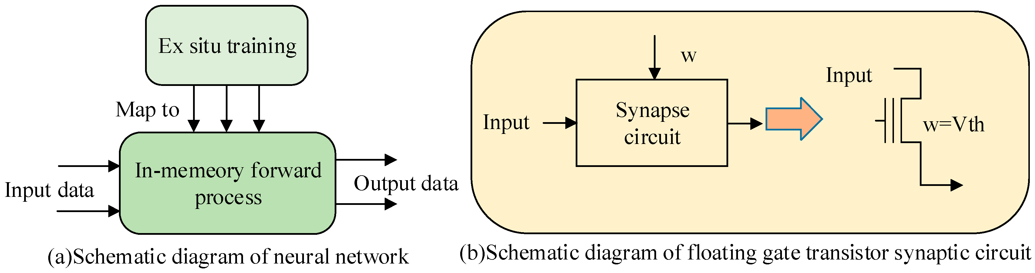
A CNN’s main operation method is Multiply Accumulate (MAC), between the weight matrix and the input matrix. The float transistor is the basic unit of NVFM, which can store and release electrons with low energy consumption. Therefore, this study will simulate the CNN synaptic structure using floating delete transistors to achieve the operational operations of neural networks [15]. Figure 1 shows the hardware implementation of the CNN and the corresponding way of simulating synapses with transistors.
Figure 1a is a schematic diagram of the CNN implementation method. The weight matrix was mapped to the synapse in the experiment, MAC forward operations were performed on the input data, and the final stored information was output. In Figure 1b, the cross array of the NVFM circuit corresponds to each neuron of the neural network, and the transistor corresponds to the synaptic circuit. Due to the role of transistors in releasing electrons, NVFM circuits will achieve free access to transistors and control data writing and erasure by reading threshold voltage [16]. The Fowler–Nordheim (F–N) tunneling effect mechanism will be used in the experiment to read the threshold voltage. This mechanism improves the efficiency of writing and erasing compared to traditional electron injection methods. The specific method is to first apply a positive high voltage to the circuit. Through the F–N tunneling effect mechanism, electrons are released and all units are erased row by row and column by column. In flash memory operations, the F–N tunneling effect occurs between the transistor bottom and the floating gate, as shown in Figure 1b. The data erasure process in non-volatile flash memory circuits such as NAND Flash involves clearing the stored data in specific memory cells or blocks. It is important to note that the erasure operation is performed on a specific block or blocks of memory cells within the NAND Flash array. Each block usually contains multiple pages or sectors. The erase operation is conducted at the block level. An entire block of memory cells is erased simultaneously. Firstly, a high voltage, referred to as the erase voltage or erase pulse, is applied to the control gate (wordline) of the selected block(s) of memory cells. The erase voltage creates a strong electric field between the control gate and the channel region of the memory cells in the block. Afterwards, under the action of an electric field, the high electric field induces a phenomenon called Channel Hot Electron (CHE) injection or Fowler–Nordheim tunneling. Electrons gain sufficient energy from the electric field and tunnel through the thin oxide layer, effectively removing the trapped charge from the floating gate. This erases the stored data. Finally, after the erase operation, the memory cells in the block are typically subjected to a verification step to ensure the successful erasure. This involves reading the cells and confirming that they have reached a predetermined erased state. Figure 2 shows the specific erasure operation of F–N tunneling.
In Figure 2, a positive high voltage of 8 V is added to the control gate WL in the selected circuit, as shown in the red circuit on the right side of the figure. Additionally, a voltage of 3 V is applied to the drain BL to make the non-volatile unit conductive. The unselected line on the left is applied with a voltage of 0 V. Then, a voltage of 0 V is applied to the selected line unit’s source SL, and a voltage of 3 V is input to the others. The gap between the control gate and the floating gate is represented as an F–N tunneling channel. Finally, an erase operation is performed. The potential difference between SL and WL as shown in the figure is 5 V. When it is greater than 0 V, it indicates that the F–N tunneling condition is not met and needs to be erased. Then, comparative erasure operations are performed line by line until all erasures are finally completed. After completing the erase operation, the voltage inside the transistor will change with the operation. Specifically, when is lower than the threshold voltage , the F–N tunneling condition is not met, and the transistor is not turned on. Equation (1) is the source leakage current expression formula at this time. For the parameter meanings, see Glossary.
In Equation (1), is the leakage current constant. stands for the voltage between the control gate and the source. stands for the threshold voltage of the transistor. stands for the current between the drain and source electrodes. stands for the gate coefficient. When is above the threshold voltage , the transistor turns on, and changes with the voltage between the drain and source. Equation (2) stands for at this time.
In Equation (2), stands for the voltage between the drain and source electrodes. stands for electron mobility. and represent the size width and length of the transistor. is the gate oxygen capacitance per unit area. When continues to increase, the transistor will no longer be linearly represented. Equation (3) is the current formula at this time.
In Equation (3), shows a parabolic trend at this time. Finally, when , reaches stability, meaning that the transistor is operating at saturation. Equation (4) stands for the at this time.
To achieve the NVFM simulation of CNN operations, simply simulating the synapses of hardware transistors cannot achieve the desired effect. It also requires the combination of hardware and software to collaborate in designing circuits for training. This study selected an IMC array for research. Figure 3 shows the approximate process of the array.
In Figure 3, after the original data is input, the three-layer neural network cross-array forward calculation will be performed first, and then the corresponding results will be output. The output value was compared with the reverse inference output value of the software. If the hardware output value is greater than the software output value, the training is successful, and the optimized results are stored. If not, the training will not converge, and the weight will be updated for the next round of calculations until all the original data are covered.
3.2. Design of CNN Cross Array Circuit Based on IMC Integrated
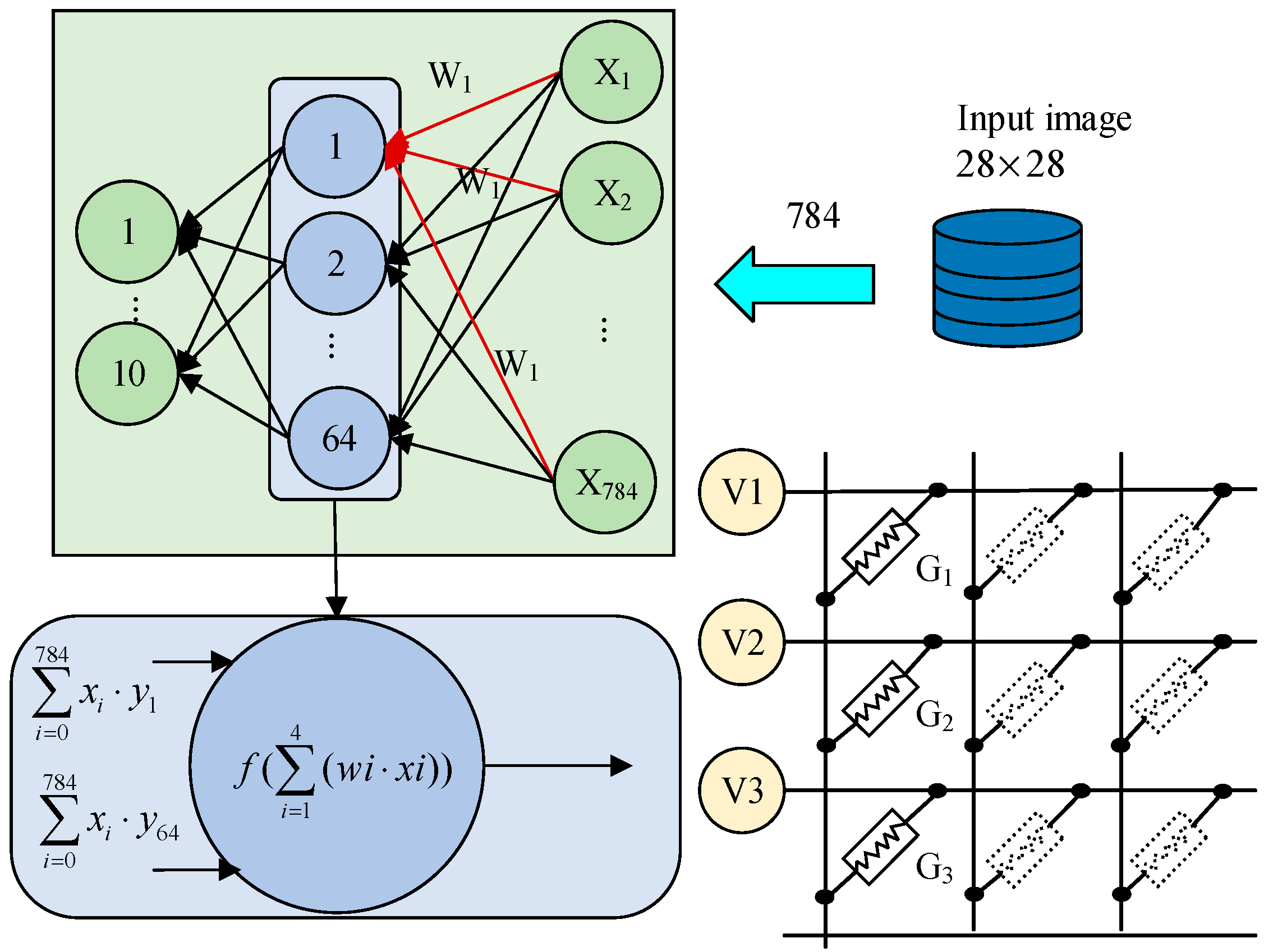
For the design of the complete IMC circuit, the research focuses on the IMC cross circuit. At the same time, peripheral circuits such as the voltage subtracter circuit, voltage follower circuit and ReLU activation function circuit are introduced to improve the overall working efficiency [17]. Whether the corresponding dataset can be identified is a classic problem in machine learning classification. The study will assume the Fashion-MNIST dataset as the experimental dataset to design a neural network cross-array structure to achieve better recognition and classification performance. Figure 4 shows the specific CNNNVFM cross-array structure.
In Figure 4, the input data resolution is 28 × 28, a total of 784 pixels. The specific neural network structure is a three-layer circuit of 784 × 64 × 10. The middle blue layer is the hidden layer circuit. The purpose of this structure is to simulate the synaptic structure of a neural network through a non-volatile unit floating-gate transistor in the vertical direction on the right and achieve the classification operations of the neural network [18,19]. In a circuit, the drain voltage stands for the salient data of the input. The threshold voltage difference in the floating-gate transistor serves as the weight of the synapse. The drain electrodes of the floating-gate unit are connected to each other and connected in parallel with the source electrode. For the optimization of the synaptic-weight matrix, the nonlinear activation function (ReLU) is introduced to select epoch parameters and learning rate. Equation (5) is the optimal weight matrix.
In Equation (5), stands for the weight matrix, and stands for the input data. stands for the ReLU function value when the input data are . To make the classification effect more obvious, this study selected Softmax function to optimize the model classification. Equation (6) is the Softmax function.
In Equation (6), and represent the -th and -th input data. stands for the -th element’s Softmax value. The model conversion of the load resistor itself will have an impact on floating-gate structure’s voltage value. The research will design a feedback loop structure to solve the voltage stability problem. Equation (7) is the mathematical expression for the output voltage of the feedback circuit differential amplifier.
In Equation (7), is the reverse terminal voltage of the amplifier. stands for the output voltage value. is the gain of the differential amplifier. is the input voltage. Equation (8) stands for the current flowing through the feedback circuit.
In Equation (8), stands for the current feedback coefficient, and is the threshold voltage of the floating-gate transistor. Formulas (7) and (8) were combined in the experiment, and was assumed. After calculation and resolution, in Equation (9) can be obtained.
In Equation (9), is the equivalent resistance value of the external load circuit. When approaches infinity, . At this point, the voltage at the same amplifier end is equal to . Figure 5 shows the ReLU activation function circuit and voltage subtracter circuit design in the peripheral circuit.
In Figure 5, the subtractor is an improved operational amplifier voltage subtractor circuit that can obtain two input voltages. It includes four load resistors, with a ground terminal voltage of 0.9 V for the grounded load resistor and an output terminal connected to the ReLU circuit. The ReLU circuit consists of a differential amplifier and a transmission gate. In the experiment, a transmission gate was used to compare the output voltage with the ground voltage to control the conduction of the transmission gate. Due to the “virtual short” and “virtual break” of the subtraction classifier port, the formula can be obtained in (10).
In Equation (10) and Figure 5, , , and represent the load resistance. and represent the current flowing through and , respectively. and are two input voltages, stands for virtual short voltage, and stands for virtual break voltage. is the ground terminal voltage, and is the output voltage. Equation (11) stands for the output voltage.
When = , = , (10) and (11) are combined to obtain Equation (12).
When = , the output voltage in Equation (13) can be obtained.
When the gain is infinite, Equation (14) stands for the output voltage of the subtractor circuit.
By combining the relevant formulas of the subtractor and the ReLU function, the output voltage in Equation (15) is ultimately obtained.
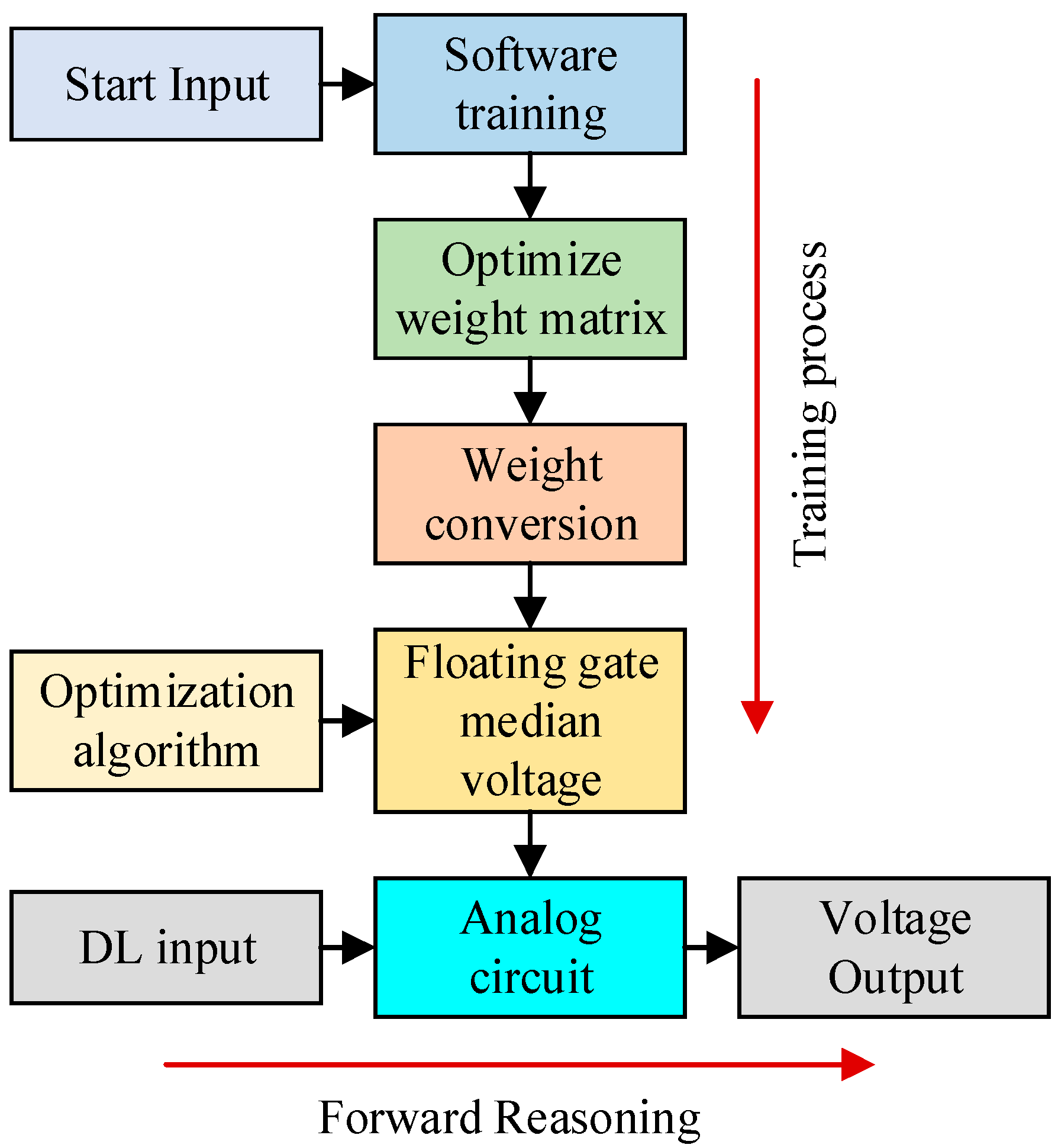
This study designed an IMC integrated method based on NVFMU to simulate neural network classifiers. Figure 6 shows the specific control process of a neural network classifier.
In Figure 6, the general process of controlling the classifier is shown as follows: first, software training was performed on the input data. Secondly, the synaptic weights of the neural network were optimized and transformed to obtain corresponding voltage prefabrication for the floating-gate transistor. Then, a voltage was applied based on the characteristic values detected by the transistor gate. Finally, forward inference was performed based on the subtractor of the analog circuit, and the classification results were output.
4. Simulation and Verification of CNN Analog Circuit Based on NVFM
This study introduced the Iris dataset to conduct simulation experiments on the designed analog circuit, verify its feasibility, and analyze its power consumption and accuracy. Finally, different neural network structures and traditional von Neumann architecture were introduced for experiments and were compared and analyzed with the IMC architecture of the NVFM CNN explored in this study.
4.1. Simulation Power Analysis of Analog Circuits
The experimental dataset used in this study is the Iris dataset, which is widely used by scholars. This dataset contains a total of 150 sets of Iris data, including three different types, namely Virginia Iris, Varicolor Iris, and Setosa Mountain Iris, with 50 sets each [20]. This experiment will conduct simulation experiments on analog circuits based on the Iris dataset. Table 1 shows the main simulation parameters.
To verify the effect of the nonlinear activation function optimized synaptic-weight method designed in this study, the experiment divided the original dataset into two equal parts. A set of optimal weight matrices obtained through training optimization is applied to analog circuits. The other group was the test group for scientific control. Accuracy and recall indicators were introduced to evaluate the experimental results in Figure 7.
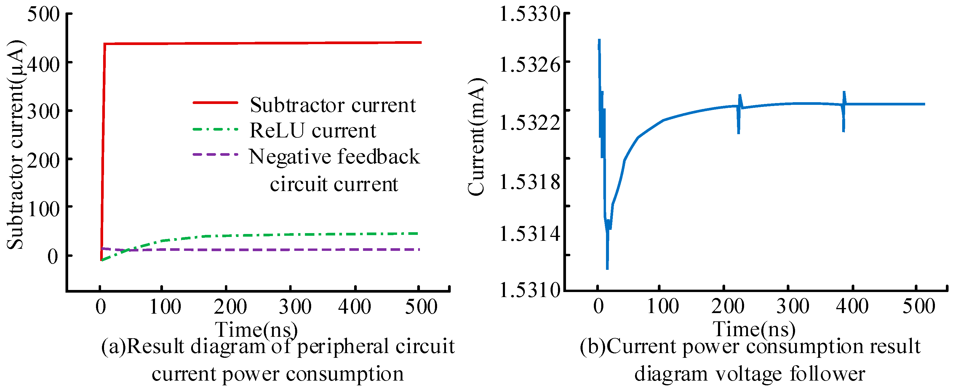
The optimal weight matrix parameters selected through the linear activation function are: Learning rate = 0.002, Epoch = 1100. Figure 7 shows the comparison results. In Figure 7a, the average accuracy of the training and testing sets is 96.2 and 95.3, respectively, and the accuracy increases with the increase in sample size. When the sample is 150 sets of data, the accuracy training set is 98.2, and the test set is 97.6. In Figure 7b, the recall rate of the experiment is also positively correlated with the number of samples, with an average recall rate of 60.2 for the training set and 58.8 for the test set. The recall rates reached 62.2 and 61.9 for a sample size of 150 groups. Optimizing the weight matrix can improve the accuracy of classification and achieve good classification results. To consider the specific power consumption of the hardware circuit in this study, the experiment analyzed the power consumption current of the core analog synaptic computing circuit and peripheral hardware circuits. Figure 8 shows the simulation results of energy consumption.
In Figure 8a, the currents of the subtractor circuit and ReLU circuit are extremely low, both of which do not exceed 100 µA and can be ignored. However, the current of the negative feedback circuit is about 440 µA compared to other peripheral circuits, but the overall current of the device is still relatively small. In Figure 8b, the current consumption of the voltage follower reaches a stable state after 400 ns, with a current of approximately 1.53 mA. Overall, the current consumption of the analog circuit mainly depends on the voltage follower. In a classification and recognition experiment, the power consumption of the voltage follower accounted for about 65% of the entire circuit power consumption. However, the overall current of the analog circuit not exceeding 2 mA is still extremely low, indicating that the method of simulating neural network synapses in this study has good performance.
4.2. Simulation Results of Analog Circuits Based on NVFMU
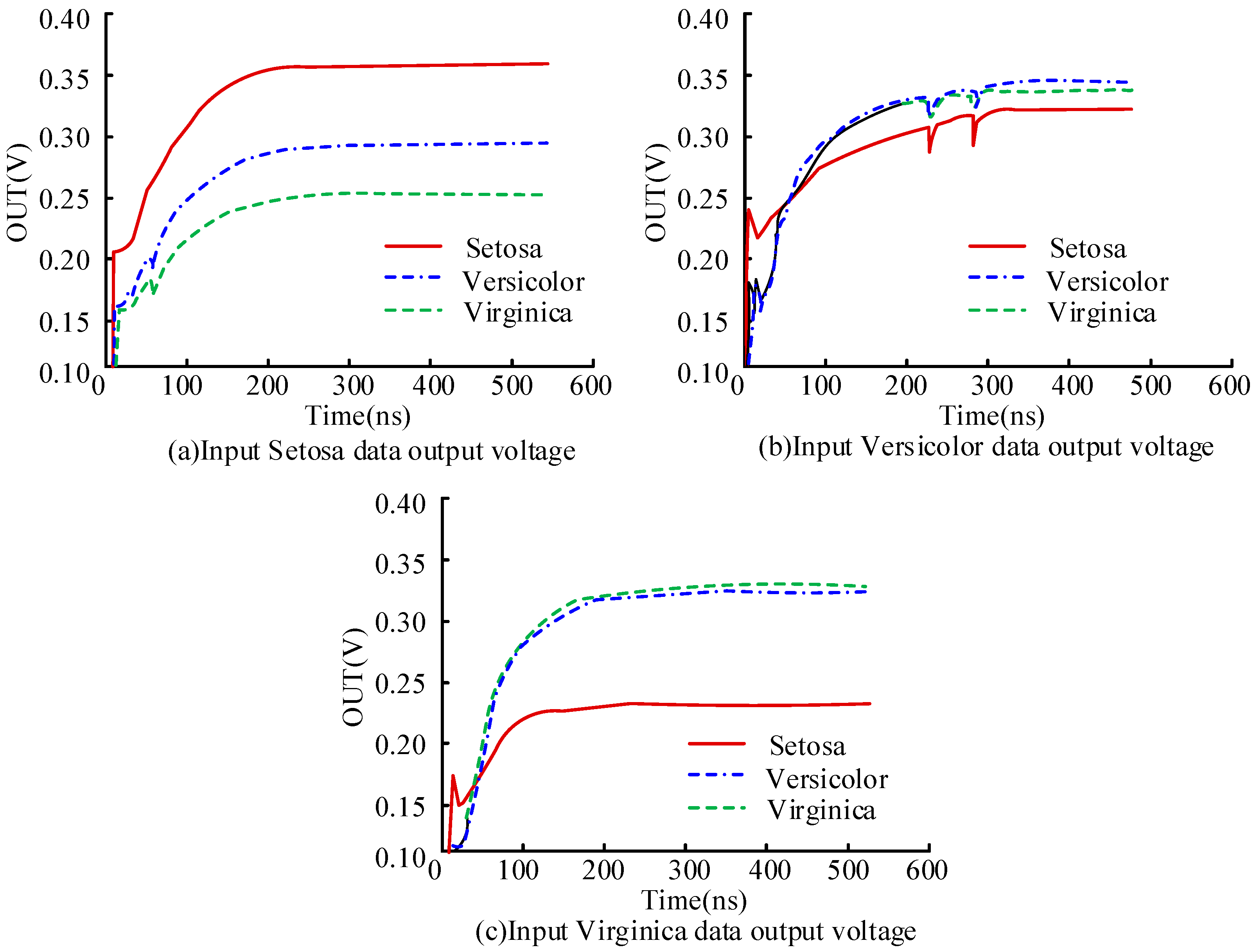
This experiment conducted simulation experiments on analog circuits using the Iris dataset as experimental data. A stable power supply voltage was input to the analog circuit, and the complete circuit was subjected to static scanning observation and classification [21,22]. Specifically, the highest voltage output value of Iris flowers is represented as the classification and recognition results of the experiment. When the three groups of Iris categories are input data, Figure 9 shows the correct classification structure for Virginia, Setosa, and Versicolor.
In Figure 9, the experiment applies a gate on voltage to the circuit at 1 ns. At this point, the circuit begins to correspond, and the classification curve undergoes strong oscillations. At approximately 100 ns, the circuit response is complete, and the curve becomes flat. Figure 8b shows a strong circuit response when the input is Versicolor data. The curve only reaches stability after 350 ns, which may be influenced by the state of the transistor and cause competition phenomenon. This causes a brief oscillation in the classification before it stabilizes, without affecting the experimental results. Overall, when the input data is a certain type of Iris, the classification effect of that type of Iris is the best. The maximum output voltage is around 0.35 V, the curve is smooth and stable, and the overall classification effect is good. Next, a simulation experiment was conducted on all 150 sets of Iris data, using the Iris species corresponding to the highest output voltage as the accurate classification result. Among them, 100 training sets and 50 test sets were set up in the experiment. In the experiment, the training set was used to calculate the optimal weights and estimate the classification of analog circuits. Figure 10 shows the experimental results of a simulation experiment on 150 sets of Iris flowers.
Among the 150 sets of data in Figure 10, Setosa’s floral features are the most obvious and the classification effect is the most intuitive. The difference in output voltage between Virginia and Versicolor is not significant, but the resulting pattern can still be distinguished. On the right side of Figure 10, even though the voltage output values of Virginia and Versicolor are equivalent, there is still a gap of nearly 10 mV. At this point, different flower patterns can be distinguished, and the overall classification effect is good. This analog circuit has certain feasibility. The simulated neural network selected for this study was CNN. The experiment further validated the impact of different neural network structures on the performance of the NVFM analog circuit studied, as well as the superiority of the IMC structure. The experiment introduced Spiking Neural Networks (SNNs) and Deep Neural Networks (DNNs) and conducted simulation experiments on the von Neumann architecture and IMC architecture, respectively, along with the CNN used in the study. Table 2 shows the results.
In Table 2, firstly, the recognition accuracy of analog circuits under the IMC architecture is slightly lower than that of the von Neumann architecture, but the difference is not significant, with all having good recognition accuracy rates of over 93%. Secondly, the IMC architecture greatly improves the recognition performance of the circuit, significantly reducing the recognition rate and current power consumption [23]. The recognition rate under the von Neumann architecture is close to 1000 μs and the IMC architecture recognition rate is 12 μs. The circuit energy consumption under the von Neumann architecture is close to 15,000 nJ, while the circuit energy consumption under the IMC architecture is only around 360 nJ. Finally, under the IMC architecture, CNN has the highest recognition accuracy and overall classification performance. Overall, the IMC architecture designed in this study can achieve accuracy comparable to traditional von Neumann architectures. This greatly reduces the circuit recognition rate and current power consumption and improves recognition efficiency. The performance of various benchmark neural network structures is comparable, with CNN structures having the highest accuracy.
5. Conclusions
In the research of improving the efficiency of neural morphology operations by simulating neural network structures in hardware circuits, the traditional von Neumann architecture has problems such as high energy consumption and low computational efficiency. This study was based on NVFMU, simulated a CNN structure, and designed an IMC integrated architecture analog computing circuit to solve related problems. This circuit uses NVFMU’s floating-gate transistor to simulate CNN synaptic structure to design a core cross-array circuit. At the same time, peripheral hardware circuits were introduced for improvement and optimization in the experiment, and the Iris dataset was selected for simulation experiments on the circuit. First, the optimal weight matrix parameters selected through the nonlinear activation function were learning rate = 0.002 and epoch = 1100. Simulation experiments were conducted under the optimal weight matrix. The average accuracy of the training set and the test set were 96.2 and 95.3, respectively, and the average recall rate was 60.2 for the training set and 58.8 for the test set. This indicates that this method can improve classification computation performance. Secondly, the analysis of the circuit power consumption results shows that the current power consumption of the subtractor circuit and ReLU circuit is extremely low, both of which do not exceed 100 µA. The power consumption of the negative feedback circuit is relatively high, at about 440 mA, but the overall power consumption is still very small. Finally, the accuracy of the relevant circuits in the IMC architecture is over 93%, the energy consumption is only about 360 nJ, and the recognition rate is about 12 μs. Compared with the traditional von Neumann architecture, it greatly reduces circuit recognition rate and current power consumption while meeting accuracy requirements, and also improves recognition efficiency.
Author Contributions
Conceptualization, P.X. and I.S.; methodology, P.X.; software, D.L.; validation, P.X. and D.L.; formal analysis, D.L.; investigation, P.X. and F.W.; data curation, I.S.; writing—original draft preparation, P.X.; writing—review and editing, I.S. All authors have read and agreed to the published version of the manuscript.
Funding
This paper is supported by the Ministry of Education University-Industry Collaborative Education Program (202101326005, 202102295003) and 2022 Innovative Experimental Teaching Project of Qingdao University.
Data Availability Statement
Not applicable.
Acknowledgments
Thank the Analysis and Testing Center of Qingdao University for providing data support for this study.
Conflicts of Interest
The authors declare no conflict of interest.
Glossary
| Parameter | Meaning |
| The voltage between the control gate and the source | |
| The threshold voltage of the transistor | |
| The current between the drain and source electrodes | |
| The gate coefficient | |
| The voltage between the drain and source electrodes | |
| Electron mobility | |
| The size width of the transistor | |
| The size length of the transistor | |
| The weight matrix | |
| The input data | |
| The -th element’s Softmax value | |
| The reverse terminal voltage of the amplifier | |
| The output voltage value | |
| The gain of the differential amplifier | |
| The input voltage | |
| The current feedback coefficient | |
| The threshold voltage of the floating-gate transistor | |
| The equivalent resistance value of the external load circuit | |
| Virtual short voltage | |
| Virtual break voltage |
References
- Liao, Y.; Gao, B.; Xu, F.; Yao, P.; Qian, H. A Compact Model of Analog RRAM with Device and Array Nonideal Effects for Neuromorphic Systems. IEEE Trans. Electron. Devices 2020, 67, 1593–1599. [Google Scholar] [CrossRef]
- Milo, V.; Zambelli, C.; Olivo, P.; Pérez, E.; Ielmini, D. Multilevel HfO2-based RRAM Devices for Low-power Neuromorphic Networks. APL Mater. 2019, 7, 081120. [Google Scholar] [CrossRef] [Green Version]
- Guan, Y.; Ohsawa, T. Co-design of Binary Processing in Memory ReRAM Array and DNN Model Optimization Algorithm. IEICE Trans. Electron. 2020, 103, 685–692. [Google Scholar] [CrossRef]
- Peurifoy, J.; Shen, Y.; Jing, L.; Yang, Y.; Cano-Renteria, F.; DeLacy, B.G.; Joannopoulos, J.D.; Tegmark, M.; Soljačić, M. Nanophotonic particle simulation and inverse design using artificial neural networks. Sci. Adv. 2018, 4, eaar4206. [Google Scholar] [CrossRef] [Green Version]
- Sheverdin, A.; Monticone, F.; Valagiannopoulos, C. Photonic inverse design with neural networks: The case of invisibility in the visible. Phys. Rev. Appl. 2020, 14, 024054. [Google Scholar] [CrossRef]
- Lee, S.; Lim, S.; Choi, N.Y.; Bae, J.H.; Lee, J.H. Operation Scheme of Multi-layer Neural Networks Using NAND Flash Memory as High-density Synaptic Devices. IEEE J. Electron. Devices Soc. 2019, 7, 1085–1093. [Google Scholar] [CrossRef]
- Park, H.; Kim, T. Speeding-up neuromorphic computation for neural networks: Structure optimization approach. Integration 2022, 82, 104–114. [Google Scholar] [CrossRef]
- Meng, J.L.; Wang, T.Y.; He, Z.Y.; Chen, L.; Zhu, H.; Ji, L.; Sun, Q.Q.; Ding, S.J.; Bao, W.Z.; Zhou, P.; et al. Flexible boron nitride-based memristor for in situ digital and analogue neuromorphic computing applications. Mater. Horiz. 2021, 8, 538–546. [Google Scholar] [CrossRef]
- Xie, Z.; Zhuge, C.; Zhao, Y.; Xiao, W.; Fu, Y.; Yang, D.; Zhang, S.; Li, Y.; Wang, Q.; Wang, Y.; et al. All-Solid-State Vertical Three-Terminal N-Type Organic Synaptic Devices for Neuromorphic Computing. Adv. Funct. Mater. 2022, 32, 310–314. [Google Scholar] [CrossRef]
- Wang, T.Y.; Meng, J.L.; Chen, L.; Zhu, H.; Sun, Q.Q.; Ding, S.J.; Bao, W.Z.; Zhang, D.W. Flexible 3D memristor array for binary storage and multi-states neuromorphic computing applications. InfoMat 2021, 3, 212–221. [Google Scholar] [CrossRef]
- Lu, J.; Li, Y.; Xuan, Z.; Xu, H.; Wu, S.; Wang, Z.; Long, S.; Liu, Q.; Shang, D. One Transistor One Electrolyte-Gated Transistor Based Spiking Neural Network for Power-Efficient Neuromorphic Computing System. Adv. Funct. Mater. 2021, 31, 210–242. [Google Scholar]
- Jang, Y.; Park, J.; Kang, J.; Lee, S.-Y. Amorphous InGaZnO (a-IGZO) synaptic transistor for neuromorphic computing. ACS Appl. Electron. Mater. 2022, 4, 1427–1448. [Google Scholar] [CrossRef]
- Shrestha, A.; Fang, H.; Mei, Z.; Rider, D.P.; Wu, Q.; Qiu, Q. A survey on neuromorphic computing: Models and hardware. IEEE Circuits Syst. Mag. 2022, 22, 6–35. [Google Scholar] [CrossRef]
- Valagiannopoulos, C.; Sarsen, A.; Alu, A. Angular memory of photonic metasurfaces. IEEE Trans. Antennas Propag. 2021, 69, 7720–7728. [Google Scholar] [CrossRef]
- Schott, S.; Bertolotti, J.; Léger, J.-F.; Bourdieu, L.; Gigan, S. Characterization of the angular memory effect of scattered light in biological tissues. Opt. Express 2015, 23, 13505–13516. [Google Scholar] [CrossRef] [Green Version]
- Demasius, K.U.; Kirschen, A.; Parkin, S. Energy-efficient memcapacitor devices for neuromorphic computing. Nat. Electron. 2021, 4, 748–756. [Google Scholar] [CrossRef]
- Rathi, N.; Chakraborty, I.; Kosta, A. Exploring neuromorphic computing based on spiking neural networks: Algorithms to hardware. ACM Comput. Surv. 2023, 55, 243. [Google Scholar] [CrossRef]
- Xu, P.; Ding, C.; Li, Z.; Yu, R.; Cui, H.; Gao, S. Photocatalytic degradation of air pollutant by modified nano titanium oxide (TiO2) in a fluidized bed photoreactor: Optimizing and kinetic modeling. Chemosphere 2023, 319, 137995. [Google Scholar] [CrossRef]
- Davies, M.; Wild, A.; Orchard, G.; Amirskaya, Y.S.; Risbud, S.R. Advancing neuromorphic computing with loihi: A survey of results and outlook. Proc. IEEE 2021, 109, 911–934. [Google Scholar] [CrossRef]
- Yazbek, H.A.; Surriya, F.; Khan, S.U.; Jan, N.; Marinkovic, D. A Novel Approach to Model the Economic Characteristics of an Organization by Interval-Valued Complex Pythagorean Fuzzy Information. J. Comput. Cogn. Eng. 2023, 2, 75–87. [Google Scholar] [CrossRef]
- Xu, P.; Yuan, Q.; Ji, W.; Zhao, Y.; Yu, R.; Su, Y.; Huo, N. Study on Electrochemical Properties of Carbon Submicron Fibers Loaded with Cobalt-Ferro Alloy and Compounds. Crystals 2023, 13, 282. [Google Scholar] [CrossRef]
- Milo, V.; Malavena, G.; Compagnoni, C.M.; Ielmini, D. Memristive and CMOS Devices for Neuromorphic Computing. Materials 2020, 13, 166. [Google Scholar] [CrossRef] [PubMed] [Green Version]
- Joshi, V.; Eleftheriou, E. Accurate Deep Neural Network Inference Using Computational Phase-change Memory. Nat. Commun. 2020, 11, 2473–2485. [Google Scholar] [CrossRef] [PubMed]
Figure 1.
Schematic diagram of the correspondence between neural networks and transistors.

Figure 2.
Schematic diagram of F–N tunneling erasure operation.

Figure 3.
Schematic diagram of integrated storage and computing training process.

Figure 4.
Deep neural network structure and corresponding cross-array structure diagram.

Figure 5.
Schematic diagram of ReLU function and voltage subtractor structure.

Figure 6.
Flow chart of classifier control method steps.

Figure 7.
Comparison chart of optimal weight experiments.

Figure 8.
Power consumption diagram of peripheral circuit and voltage follower.

Figure 9.
Simulation results of Iris classification.

Figure 10.
Iris simulation result diagram.


Table 1.
Analog circuit simulation parameter table.
| Parameter | Parameter Value |
|---|---|
| Transistor size | 220/180 |
| Supply voltage | 1.8 |
| Reference source level | 1.0(1/2VDD) |
| Gate WL voltage | 1.0(1/2VDD) |
| Iris circuit load resistance | 4 |
| MNIST circuit load resistance | 220 |
Table 2.
Classification results of different neural network structures.
| Von Neumann Architecture | Integrated Storage and Computing Architecture | |||||
|---|---|---|---|---|---|---|
| Network | CNN | DNN | SNN | CNN | DNN | SNN |
| Accuracy (%) | 97.93 | 98.33 | 95.98 | 95.64 | 94.27 | 93.80 |
| Recognition rate (μs) | 1000.00 | 964.00 | 897.00 | 12.56 | 11.67 | 12.92 |
| Energy consumption/nJ | 146,700 | 14,900 | 15,000 | 360 | 354 | 357 |
Disclaimer/Publisher’s Note: The statements, opinions and data contained in all publications are solely those of the individual author(s) and contributor(s) and not of MDPI and/or the editor(s). MDPI and/or the editor(s) disclaim responsibility for any injury to people or property resulting from any ideas, methods, instructions or products referred to in the content. |
© 2023 by the authors. Licensee MDPI, Basel, Switzerland. This article is an open access article distributed under the terms and conditions of the Creative Commons Attribution (CC BY) license (https://creativecommons.org/licenses/by/4.0/).
Share and Cite
MDPI and ACS Style
Xu, P.; Lan, D.; Wang, F.; Shin, I. In-Memory Computing Integrated Structure Circuit Based on Nonvolatile Flash Memory Unit. Electronics 2023, 12, 3155. https://doi.org/10.3390/electronics12143155
AMA Style
Xu P, Lan D, Wang F, Shin I. In-Memory Computing Integrated Structure Circuit Based on Nonvolatile Flash Memory Unit. Electronics. 2023; 12(14):3155. https://doi.org/10.3390/electronics12143155
Chicago/Turabian StyleXu, Peilong, Dan Lan, Fengyun Wang, and Incheol Shin. 2023. "In-Memory Computing Integrated Structure Circuit Based on Nonvolatile Flash Memory Unit" Electronics 12, no. 14: 3155. https://doi.org/10.3390/electronics12143155
Note that from the first issue of 2016, this journal uses article numbers instead of page numbers. See further details here.