
High Step-Up Converter


Department of Electrical Engineering, National Taipei University of Technology, 1, Sec. 3, Zhongxiao E. Rd., Taipei 10608, Taiwan
*
Author to whom correspondence should be addressed.
Electronics 2023, 12(19), 4000; https://doi.org/10.3390/electronics12194000
Submission received: 18 August 2023
/
Revised: 19 September 2023
/
Accepted: 19 September 2023
/
Published: 22 September 2023
(This article belongs to the Special Issue Artificial Intelligence Chip and Advanced Integrated Circuit Design)
Abstract
:A new high-boost converter derived from a charge-pump capacitor-based dual-boost converter is presented herein. Compared with the existing charge-pump capacitor-based dual-boost inductor converter, this structure adds an additional voltage-doubling circuit and additional coil to the original circuit to increase the voltage conversion ratio and winds the three coils around the same magnetic element. By this way, the overall size of the circuit can be reduced, and the leakage energy of the coupled inductor can be recovered. In this paper, the proposed new high-boost converter is firstly explained and analyzed, followed by simulations to demonstrate the feasibility of the proposed circuit and finally the experimental results to verify its effectiveness.
1. Introduction
Nowadays, most countries need to adopt large-scale construction of power generation methods, such as thermal power generation, nuclear power generation, and hydroelectric power generation, in order to obtain the electricity needed for daily life. Although these methods have the advantage of obtaining lower electricity prices, they are often limited by location. For example, thermal power generation needs to be located far away from cities to prevent air pollution, hydroelectric power generation needs to be located in places where there is a source of water, and nuclear power generation has to be located at the seacoast to use seawater for cooling. In the past, the cost of setting up these large-scale power plants was very high, but in recent years, due to the improvement of power generation reliability, the cost of setting up the plants has been lower than the cost of maintaining the power grid, so many countries have invested in the research and development of microgrids and decentralized power generation technology. There are several types of decentralized power generation, such as waste heat, solar power, grid-supplied electricity from electric vehicles, and wind power. However, the voltages generated by the above power generation methods are not high and stable enough, and in addition, the output voltage is prone to change with the change of load. To solve this problem, a step-up converter is connected to the back end of the decentralized energy source to provide a relatively stable and high voltage for the back-end equipment or to provide the input power for the inverter of the utility paralleling system, which is needed for the power supply. For example, in the thermoelectric generator (TEG), stand-alone solar power system [1], and utility-parallel solar power system [2], a step-up converter is required to step up the low voltage generated by the thermoelectric modules or solar panels to a high voltage to provide power to the inverter or load.
Generally speaking, the voltage conversion ratio of a conventional boost converter is theoretically infinite, but due to the parasitic components, it can only be increased to about four times [3]. Therefore, many novel boost converters have been proposed, such as the KY converter and its related derivatives [4,5,6,7], which operate on the principle of obtaining a high voltage conversion ratio by means of a simple charge-pump circuit with a boost inductor or coupled inductor. In the literature [8,9,10,11,12], charge-pump circuits with single or multiple magnetic components are used to improve the voltage conversion ratio. The literature [13,14,15,16] proposes interleaved boost circuits to reduce the relatively large input currents; the main principle is also the use of coupled inductors to achieve high voltage conversion ratios. The literature [13] presents a variant of the interleaved boost converter, which is characterized by bidirectional energy conversion. The disadvantage is that the number of controllable switching elements is too large and hence the control is complicated. The literature [14] proposes a high-boost converter, which has the advantage of simple structure. The literature [15] presents an interleaved boost converter characterized by an ultra-high boost ratio. The literature [16] proposes also an interleaved high-boost converter, which is characterized by inductive coupling and voltage superposition to realize a high-boost function.
All the proposed structures have higher voltage conversion ratios than conventional boost converters, but each has their own drawbacks. In the literature [4,5,6,7,9], although the structures are simple and easy to implement, the voltage conversion ratios are still not high enough, and the reason is that the voltage conversion ratios presented by references [4,7,9] have the same denominator of (1 − D), where D is the duty cycle and locates between 0 and 1. But, the numerators of [4,7,9] are 1 + D, 3, and 1 + D + n, respectively, where n is the turns ratio and generally locates between 1 and 3 to reduce leakage inductances. In the literature [4,6,7,8,9,10], the converters have floating switches, which require the use of additional isolation drivers, leading to an increase in cost. In the literature [9,10,11,12], the design is not easy, and the cost is too high due to the use of too many components. In the literature [4,8,9,11,12,13,14,16], the converters use the turns ratios of the coupled inductors to increase the voltage conversion ratios; however, there is a leakage problem of the coupled inductor, which is easy to resonate with the parasitic capacitance of the switch or diode, and hence, it is easy to cause a too large voltage spike on the switch or diode. Consequently, it is necessary to select components with higher voltage ratings or add additional buffers to overcome this drawback, which makes the circuit difficult to realize. In the literature [7,16,17,18,19,20,21], multiple voltage-doubling circuits are used to achieve higher voltage conversion ratios, resulting in an increase in the number of diodes and capacitors.
The high-boost converter proposed in this paper is derived from a charge-pump capacitor-based dual-boost converter [22]. Figure 1 shows the circuit structure of the charge-pump capacitor-based dual-boost inductor converter, which consists of two inductors, two diodes, two energy-transferring capacitors, one switch, one output diode, one output capacitor, and one load resistor. The voltage conversion ratio of Vo/Vi = 2/(1 − D) is not high, so the purpose of the circuit proposed in this paper is to improve the voltage conversion ratio of this converter based on three coils wound together with the energy stored in the leakage inductance recycled.
2. Proposed High-Boost Converter
2.1. Topology Description
Figure 2 shows the proposed high-boost converter, which consists of one switch, S1; five diodes, D1, D2, D3, D4, and D5; one energy-transferring capacitor, Ce; three stabilizing capacitors, C1, C2, and C3; and one coupled inductor consisting of one primary-side winding N1, one secondary-side winding N2, one tertiary-side winding N3, and one magnetizing inductor Lm. As for the load, it is represented by the output resistance Ro.
2.2. Operating Principles
Prior to analyzing the circuit operation, the relevant symbols and their assumptions are briefly explained: (i) the input voltage and current are denoted by Vi and ii, respectively; (ii) the output voltage is signified by Vo; (iii) the capacitance of the energy-transferring capacitor Ce and voltage-stabilizing capacitors C1, C2, and C3 are large enough so that the voltages across them are maintained at some certain values; (iv) the switching period is indicated by Ts; (v) the turns ratio n is defined to be N3/N1 = N3/N2; (vi) all the switches, diodes, and capacitors are regarded as ideal components; and (vii) the circuit is operated in the continuous conduction mode (CCM), and there are ten operating states over one switching period, as in Figure 3.
On the other hand, the voltages on and currents in components are defined as follows: (i) the gate driving signal for and voltage across on S1 are represented by vgs1 and vds1, respectively; (ii) the voltages on D1, D2, D3, D4, and D5 are expressed by vD1, vD2, vD3, vD4, and vD5, respectively; (iii) the voltages across C1, C2, C3, and Ce are signified by VC1, VC2, VC3, and VCe, respectively; (iv) the voltages on N1, N2, N3, and Lm are denoted by vN1, vN2, vN3, and vN3, respectively; (v) the currents in N1, N2, N3, Lm, and Lk3 are indicated by iN1, iN2, iN3, iLm, and iLk3, respectively; and (vi) the currents in C1, C2, C3, and Ce are iC1, iC2, iC3, and iCe, respectively.
2.2.1. State 1: []
As shown in Figure 3 and Figure 4, the switch S1 is on, the diodes D1, D2, and D5 are on, and the diodes D3 and D4 are off. At the same time, the input voltage Vi charges the energy-transferring capacitor Ce, the energy stored in the leakage inductor Lk3 continues to charge the stabilizing capacitor C3, and the stabilizing capacitors C1 and C2 provide energy to the load. At t = t1, the magnetizing inductor Lm changes from demagnetization status to magnetization status. Once the stabilizing capacitor C3 stops charging, state 1 comes to an end.
2.2.2. State 2: []
As shown in Figure 3 and Figure 5, the switch S1 is still on, the diodes D1, D2, and D5 are still on, and the diodes D3 and D4 are off. At the same time, the voltage across the magnetizing inductor Lm, called vN3, equal to nVi, is the mapped voltage from the primary side to the tertiary side, so the magnetizing inductor Lm is excited, the energy-transferring capacitor Ce is still in the state of charging, and the energy required by the load is supplied by the leakage inductor Lk3, the voltage-stabilizing capacitors C1, C2, and C3, and the load. At t = t2, the leakage inductor Lk3 has finished releasing energy, proceeding to state 2.
2.2.3. State 3: []
As shown in Figure 3 and Figure 6, the switch S1 is still on, the diodes D1, D2, and D4 are on, and the diodes D3 and D5 are cut off. At the same time, the magnetizing inductor Lm is still in the state of excitation and the energy required by the load is supplied by the voltage-stabilizing capacitors C1, C2, and C3. Once the voltage-stabilizing capacitor C2 stops supplying energy to the load, state 3 comes to an end.
2.2.4. State 4: []
As shown in Figure 3 and Figure 7, the switch S1 is still on, the diodes D1, D2, and D4 are still on, and the diodes D3 and D5 are still off. At the same time, the voltage-stabilizing capacitor C2 is charging and the operating behavior of the other components is the same as that of state 3. Once the energy-transferring capacitor Ce stops charging, state 4 ends.
2.2.5. State 5: []
As shown in Figure 3 and Figure 8, the switch S1 is cut off, the diodes D3 and D4 are conducted, and the diodes D1, D2, and D5 are cut off. At the same time, the voltage across the magnetizing inductor Lm, called vN3, equal to , and hence, Lm is demagnetized, the energy-transfer capacitor Ce discharges and charges the voltage-stabilizing capacitor C1, the energy stored in the leakage inductors Lk1, Lk2, and Lk3 release the energy to the load, and the energy required by the load is supplied by the input voltage Vi, the energy-transferring capacitor Ce, the magnetizing inductor Lm, and the voltage-stabilizing capacitor C3. At t = t5, the voltage-stabilizing capacitor C2 stops charging, proceeding to state 5.
2.2.6. State 6: []
As shown in Figure 3 and Figure 9, the switch S1 is still off, the diodes D3 and D4 are conducted, and the diodes D1, D2, and D5 are cut off. The voltage-stabilizing capacitor C2 releases energy to the load, and the operating behavior of the other components is the same as that of state 5. At t = t6, state 6 ends.
2.2.7. State 7: []
2.2.8. State 8: []
As shown in Figure 3 and Figure 10, the switch S1 is still off, the diodes D3 and D5 are conducted, and the diodes D1, D2, and D4 are cut off. At the same time, the magnetizing inductor Lm charges the voltage-stabilizing capacitor C3, while the energy required for the load is supplied by the input voltage Vi, the energy-transfer capacitor Ce, the magnetizing inductor Lm, and the voltage-stabilizing capacitor C2. The moment the energy-transferring capacitor C1 stops charging, state 8 ends.
2.2.9. State 9: []
As shown in Figure 3 and Figure 11, the switch S1 is cut off, the diodes D3 and D5 are conducted, and the diodes D1, D2, and D4 are cut off. The magnetizing inductor Lm charges the voltage-stabilizing capacitor C3. At the same time, the energy required by the load is supplied by the input voltage Vi, the energy-transferring capacitor Ce, the magnetizing inductor Lm, and the voltage-stabilizing capacitors C1 and C2. The moment the energy-transferring capacitor Ce stops supplying energy to the load, state 9 comes to an end.
2.2.10. State 10: []
As shown in Figure 3 and Figure 12, the switch S1 is cut off, the diodes D1, D2, D3, and D4 are cut off, and the diode D5 is still on. At the same time, the magnetizing inductor Lm charges the voltage-stabilizing capacitor C3 and, together with the voltage-stabilizing capacitors C1 and C2, provides the energy required by the load. Once the switch S1 is turned on, state 10 ends and returns to state 1, completing one cycle.
In order to simplify the analysis, the leakage inductances Lk1, Lk2, and Lk3 are not taken into consideration, so states 1, 2, 5, and 6 can be ignored.
2.3. Voltage Gain
From Figure 9, Figure 10, Figure 11 and Figure 12, the corresponding equations for states 7, 8, 9, and 10 are as follows:
where
Therefore, (2) can be rewritten as
Since the voltage across the magnetizing inductor Lm must obey the volt–second balance in the steady state, the following can be obtained:
After rearranging (5), the following can be obtained:
The output voltage is superimposed by the voltages across three voltage-stabilizing capacitors C1, C2, and C3, that is,
By substituting (1), (4), and (6) into (7), the following can be obtained:
Substituting (6) into (8) yields
2.4. Boundary Curve between Operating Modes of Lm
Assume that the converter has no loss in power conversion, i.e., . Accordingly, by using (9), the input current can be expressed as
where
Therefore, (10) can be rewritten as
The average value of the magnetizing inductor current iLm is
Since the capacitor is equivalent to an open circuit under DC analysis, (13) can be rewritten as
The transformer characteristics can be used to obtain a relationship between IN1, IN2, and IN3:
By substituting (14) into (15), the following can be obtained:
Since turns N1 and N2 are identical, that is, , (16) can be rewritten as
The average value of input current ii is
According to the ampere–second balance, the average value of the current flowing through the capacitor Ce, called ICe, can be regarded as zero, so (18) can be rewritten as
By substituting Equation (19) into (17), the following can be obtained:
Finally, substituting (12) into (20) yields
The current ripple flowing through the magnetizing inductor Lm can be expressed as
Therefore, as , the magnetizing inductor Lm will be operated in the continuous conduction mode (CCM):
where and .
From (23), if , then the magnetizing inductor Lm operates in CCM; otherwise, it operates in the discontinuous current mode (DCM). Therefore, the boundary curve between CCM and DCM can be drawn as shown in Figure 13.
3. System and Component Specifications
Figure 14 shows the system configuration of the proposed high-boost converter, which consists of the main power stage and the negative-feedback control circuit. The main power stage is built up by a charge-pump capacitor-based dual-boost converter with three coils wound together. The feedback control circuit is composed of a voltage divider to obtain an analog signal of the output voltage, which is converted into a digital signal by an analog-to-digital converter (ADC), and then passed to an FPGA for computation to obtain the corresponding gate driving signal for the switch S1 after a low-side gate driver.
The system and component specifications are as follows: (i) the input voltage is 12 V; (ii) the output voltage is 120 V; (iii) the rated output current is 0.5 A and the minimum output current is 0.05 A; (iv) the switching frequency is 100 kHz; (v) the product name of the switch S1 is STP120NF10; (vi) the product name of the diodes D1 and D2 is MBRH2060CT; (vii) the product name of the diodes D3, D4, and D5 is V20120C; (viii) the product name of the energy-transferring capacitor Ce is Rubycon with 470 µF; (ix) the product name of the voltage-stabilizing capacitors C1, C2, and C3 is Rubycon with 100 µF; and (x) the product name of the FPGA is EP1C3T100.
4. Design Considerations
Table 1 shows the specifications of the proposed converter.
Since the general step-up-converter conversion ratio can theoretically be infinitely large but the elements have parasitic components, resulting in duty-cycle restrictions, the maximum of only operating the duty cycle is generally set at 0.6~0.7, which will be used in the design of the coupled inductor. Therefore, some system specifications can be substituted into (24) to obtain the turns ratio n:
In order to facilitate winding the coupled inductor, the turns ratio is taken as an integer:
By substituting (25) and some system specifications into (9), the corresponding duty cycle D can be obtained as
The design of the coupled inductor is based on substituting the results of (25) and (26) into (23), and the magnetizing inductance of 300 μH is selected with the core named PC44PQ26/25Z-12.
5. Simulated Waveforms
The open-loop simulation of the proposed converter, under the condition of the rated output power of 60 W, was carried out to verify the feasibility of the proposed converter by using the obtained parameters shown in Table 1 and the PSIM 9.0 software. Figure 15 shows the simulated circuit of the proposed converter. Figure 16, Figure 17, Figure 18, Figure 19 and Figure 20 show the corresponding simulated waveforms.
As shown in Figure 19, the voltage on the energy-transferring capacitor Ce is stable at a certain value, and during the switch S1 cut-off instant, the energy stored in the leakage inductance releases the energy to the load and charges the voltage-stabilizing capacitor C1, so the current of the energy-transferring capacitor Ce, called iCe, will have a current surge. As shown in Figure 20, the voltage-stabilizing capacitors C1, C2, and C3 are stable at some certain values. Therefore, the feasibility of the proposed structure is verified.
6. Measured Waveforms
The closed-loop experiment of the proposed converter, under the conditions of the minimum, half, and rated, was carried out to demonstrate the effectiveness of the proposed converter.
6.1. Steady-State Waveforms
Figure 21, Figure 22, Figure 23, Figure 24, Figure 25, Figure 26, Figure 27, Figure 28, Figure 29, Figure 30, Figure 31, Figure 32, Figure 33, Figure 34 and Figure 35 show the experimental waveforms to demonstrate the effectiveness of the proposed converter.
From Figure 21, Figure 22, Figure 26, Figure 27, Figure 31 and Figure 32, it can be seen that the voltage surge of the switch S1 and the voltage surges of the diodes D1, D2, D3, D4 and D5 will increase as the load increases, where the ringing phenomena of the diodes D1 and D2 are caused by the resonances of the parasitic capacitances of the diodes D1 and D2 with the leakage inductances of the coupled inductor and the parasitic inductance of the line when the switch S1 is turned on. However, the simulation does not consider these two parasitic capacitances, so this phenomenon does not happen.
From Figure 24, Figure 25, Figure 29, Figure 30, Figure 34 and Figure 35, it can be seen that the voltage on the energy-transferring capacitor Ce, called VCe, and the voltage on the voltage-stabilizing capacitors C1, C2, and C3, called VC1, VC2, and VC3, respectively, are all approximately stable at certain values under any load. From Figure 23, Figure 28 and Figure 33, it can be seen that the current in the primary winding iN1, the current in the secondary winding iN2, and the current in the leakage inductance Lk3, called iLk3, will increase with the increase in the load current. As the switch S1 is turned on, the part of the slope of the leakage inductance current iLk3 will be negative at light load, which is different from the negative slope of the current at half load and the positive slope of the current at rated load. The reason is that the voltage-stabilizing capacitor C2 generates a larger current during charging, which results in a smaller slope of the current in the primary winding iN1 and the secondary winding iN2. Since and and the slope of the magnetizing current iLm does not change with the load, the slope of the leakage inductance current iLk3 at the light load and the medium load will be in the negative form. From Figure 26, Figure 29 and Figure 34, it can be seen that at the turn-on moment of the switch S1, the input voltage Vi charges the energy-transferring capacitor Ce, and at the cut-off moment of the switch S1, the energy stored in the leakage inductance releases the energy to the load and charges the regulator capacitor C1, so the energy-transferring capacitor current iCe will generate current spikes at both the on and off moments of the switch S1.
In summary, from the measured steady-state waveforms, it can be seen that the behavior of the proposed structure is consistent with the results of the analysis and simulation, so the effectiveness of the proposed structure is verified.
6.2. Dynamic Waveforms
Figure 36, Figure 37, Figure 38, Figure 39, Figure 40 and Figure 41 show the load transient responses.
Figure 36 and Figure 37 show the voltage responses due to the upload change from light load to half load and download change from half load to light load, respectively. As can be seen from Figure 36 and Figure 37, the corresponding output-voltage variations are about 6% and the corresponding recovery time is about between 50 ms and 60 ms. Figure 38 and Figure 39 show the output-voltage responses due to the upload change from half load to rated load and download change from rated load to half load, respectively. As can be seen from Figure 38 and Figure 39, the corresponding output-voltage variations are about 5% and the corresponding recovery time is about 50 ms. Figure 40 and Figure 41 show the output-voltage responses due to the upload change from light load to rated load and download change from rated load to light load, respectively. As can be seen from Figure 40 and Figure 41, the corresponding output-voltage variations are about 12% and the corresponding recovery time is about 65 ms. From these figures, it can be seen that the more the load change is, the more voltage variation and the larger the recovery time.
6.3. Efficiency Measurement
Figure 42 shows the block diagram of efficiency measurement. A shunt resistor is connected in series with the input-current path, and a digital meter (Fluke 8050A) is used to measure the voltage on this resistor to obtain the input-current value, and a digital meter (Fluke 179) is used to measure the input voltage to obtain the input power. On the output side, an electronic load (Prodigit 3314F) is used to provide the load current required by the converter, and the output voltage is measured using a digital meter (Fluke 179) to obtain the output power. Eventually, the resulting input and output powers are used to calculate the efficiency of the actual circuit operation. Figure 43 shows the curve of efficiency versus load current.
From Figure 43, it can be seen that the efficiency under any load is above 89.4%, and the maximum efficiency is 92.61%.
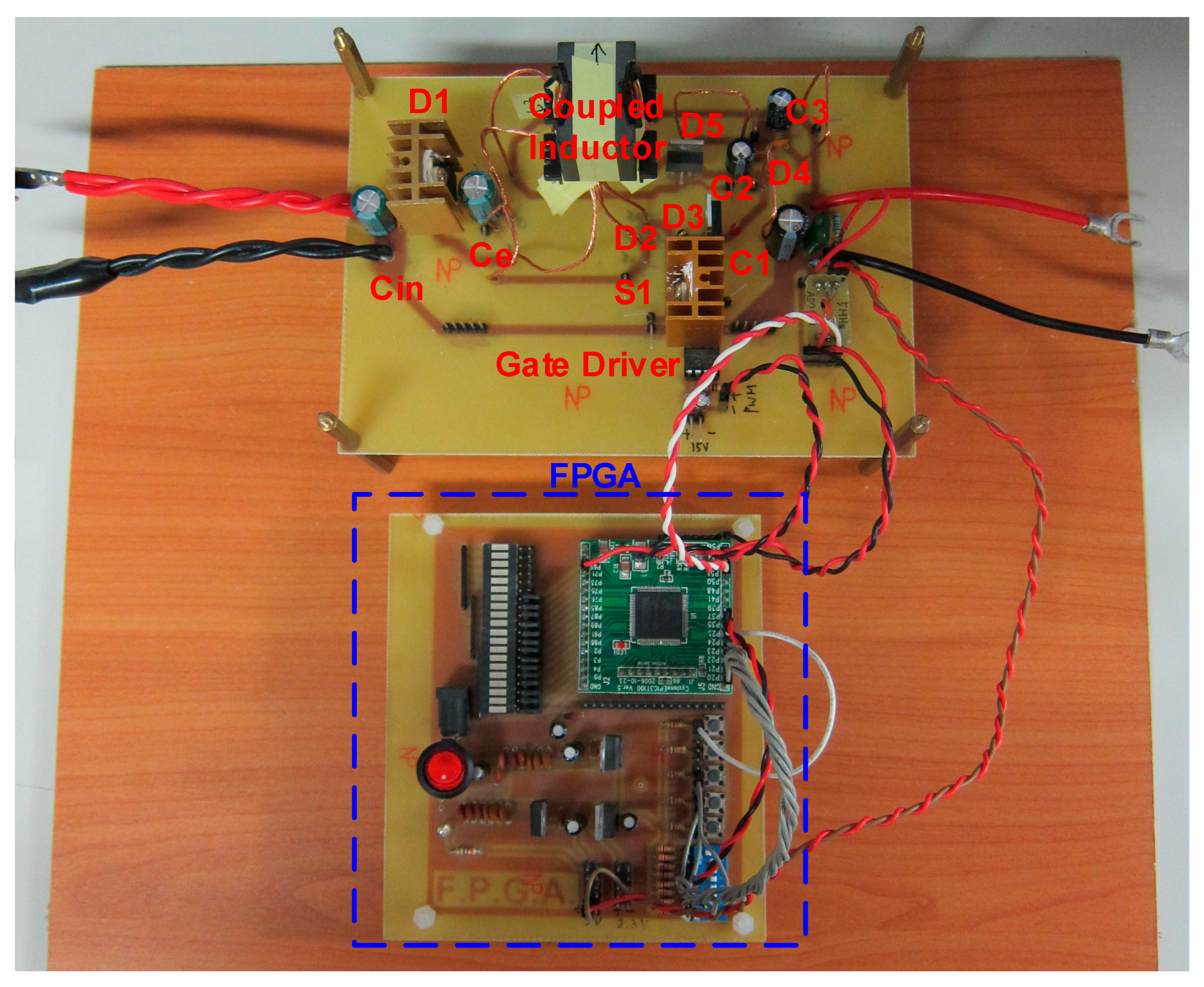
6.4. Experimental Setup
Figure 44 displays a photo of the experimental setup.
7. Circuit Comparison
Table 2 displays a comparison of the existing and proposed converters. In this table, the comparison items are in terms of CCM voltage gain, total number of components, number of diodes, number of inductors, switching frequency, and efficiency. The proposed converter has a relatively small number of components and a relatively linear voltage gain. But, because the switching frequency of the proposed converter is relatively high, the corresponding efficiency is relatively low.
8. Conclusions
In this paper, a new high-boost converter is proposed, whose main structure is improved based on the converter with a charge-pump capacitor and dual-boost inductor. This structure is made by adding an additional voltage doubler and a set of coils to the existing circuit to increase the voltage conversion ratio, and three coils are wound on the same magnetic core, reducing the overall circuit size. In addition, the energy stored in the leakage inductance of the coupled inductor can be recovered. Accordingly, the efficiency can be up to 92.61%.
Author Contributions
Conceptualization, K.-I.H. and P.-C.T.; methodology, K.-I.H. and P.-C.T.; software, P.-C.T.; validation, K.-I.H. and P.-C.T.; formal analysis, P.-C.T.; investigation, P.-C.T.; resources, K.-I.H.; data curation, P.-C.T.; writing—original draft preparation, K.-I.H.; writing—review and editing, K.-I.H.; visualization, P.-C.T.; supervision, K.-I.H.; project administration, K.-I.H.; funding acquisition, K.-I.H. All authors have read and agreed to the published version of the manuscript.
Funding
This research was funded by the Ministry of Science and Technology, Taiwan, under the grant number NSTC 112-2221-E-027-015-MY2.
Data Availability Statement
No new data were created or analyzed in this study. Data sharing is not applicable to this article.
Conflicts of Interest
The authors declare no conflict of interest.
References
- Gules, R.; Pacheco, J.D.P.; Hey, H.L.; Imhoff, J. A maximum power point tracking system with parallel connection for PV stand-alone applications. IEEE Trans. Power Electron. 2008, 55, 2674–2683. [Google Scholar] [CrossRef]
- Wu, Y.E.; Shen, C.L. Implementation of a DC power system with PV grid-connection and active power filtering. In Proceedings of the 2nd International Symposium on Power Electronics for Distributed Generation Systems, Hefei, China, 16–18 June 2010; pp. 116–121. [Google Scholar]
- Erickson, R.W.; Maksimovic, D. Fundamentals of Power Electronics, 2nd ed.; Kluwer Academic Publishers: Norwell, MA, USA, 2001. [Google Scholar]
- Sarvghadi, P.; Varjani, A.Y.; Shahparasti, M. A high step-up transformerless DC-DC converter with new voltage multiplier cell topology and coupled inductor. IEEE Trans. Ind. Electron. 2022, 69, 10162–10171. [Google Scholar] [CrossRef]
- Abkenar, P.P.; Samimi, M.H.; Marzoughi, A.; Samavatian, V.; Iman-Eini, H.; Naghibzadeh, Y. A highly reliable low-cost single-switch resonant DC-DC converter with high gain and low component count. IEEE Trans. Ind. Electron. 2023, 70, 2556–2565. [Google Scholar] [CrossRef]
- Wang, Z.; Zheng, Z.; Li, C. A high-step-up low-ripple and high-efficiency DC-DC converter for fuel-cell vehicles. IEEE Trans. Power Electron. 2022, 37, 3555–3569. [Google Scholar] [CrossRef]
- Bheemraj, T.S.; Kumar, Y.A.; Karthikeyan, V.; Pragaspathy, S. A Hybrid Structured High Step-Up DC–DC Converter for Integration of Energy Storage Systems in Military Applications. IEEE Trans. Circuits Syst. II Express Briefs 2023, 70, 1545–1549. [Google Scholar] [CrossRef]
- Hasanpour, S.; Siwakoti, Y.P.; Blaabjerg, F. A new soft-switched high step-up trans-inverse DC/DC converter based on built-in transformer. IEEE Open J. Power Electron. 2023, 4, 381–394. [Google Scholar] [CrossRef]
- Yu, L.; Wang, L.; Yang, C.; Zhu, L.; Gan, Y.; Zhang, H. A novel nonisolated GaN-based bidirectional DC-DC converter with high voltage gain. IEEE Trans. Ind. Electron. 2022, 69, 9052–9063. [Google Scholar] [CrossRef]
- Kong, I.-B.; Kim, W.-S.; Lee, S.-W. A novel high-voltage-gain quasi-resonant DC-DC converter with active-clamp and switched-capacitor techniques. IEEE Trans. Power Electron. 2023, 38, 7810–7820. [Google Scholar] [CrossRef]
- Ding, X.; Zhou, M.; Cao, Y.; Li, B.; Sun, Y.; Hu, X. A high step-up coupled-inductor-integrated DC-DC multilevel boost converter with continuous input current. IEEE J. Emerg. Sel. Top. Power Electron. 2022, 10, 7346–7360. [Google Scholar] [CrossRef]
- Zhang, M.; Wei, Z.; Zhou, M.; Wang, F.; Cao, Y.; Quan, L. A high step-up DC-DC converter with switched-capacitor and coupled-inductor techniques. IEEE J. Emerg. Sel. Top. Ind. Electron. 2022, 3, 1067–1076. [Google Scholar] [CrossRef]
- Mohammadi, M.R.; Amoorezaei, A.; Khajehoddin, S.A.; Moez, K. A high step-up/step-down LVS-parallel HVS-series ZVS bidirectional converter with coupled inductors. IEEE Trans. Power Electron. 2022, 37, 1945–1961. [Google Scholar]
- Mohseni, P.; Rahimpour, S.; Dezhbord, M.; Islam, M.R.; Muttaqi, K.M. An optimal structure for high step-up nonisolated DC-DC converters with soft-switching capability and zero input current ripple. IEEE Trans. Ind. Electron. 2022, 69, 4676–4686. [Google Scholar] [CrossRef]
- Selvam, S.; Sannasy, M.; Sridharan, M. Analysis and design of two-switch enhanced gain SEPIC converter. IEEE Trans. Ind. Appl. 2023, 59, 3552–3561. [Google Scholar] [CrossRef]
- Vaghela, M.A.; Mulla, M.A. High step-up gain converter based on two-phase interleaved coupled inductor without right-hand plane zero. IEEE Trans. Power Electron. 2023, 38, 5911–5927. [Google Scholar] [CrossRef]
- Pirpoor, S.; Rahimpour, S.; Andi, M.; Kanagaraj, N.; Pirouzi, S.; Mohammed, A.H. A novel and high-gain switched-capacitor and switched-inductor-based DC/DC boost converter with low input current ripple and mitigated voltage stresses. IEEE Access 2022, 10, 32782–32802. [Google Scholar] [CrossRef]
- Hasanpour, S.; Nouri, T.; Blaabjerg, F.; Siwakoti, Y.P. High step-up SEPIC-based trans-inverse DC-DC vonverter with quasi-resonance operation for renewable energy applications. IEEE Trans. Ind. Electron. 2023, 70, 485–497. [Google Scholar] [CrossRef]
- Hasanpour, S. New structure of single-switch ultra-high-gain DC/DC converter for renewable energy applications. IEEE Trans. Power Electron. 2022, 37, 12715–12728. [Google Scholar] [CrossRef]
- Harini, S.; Chellammal, N.; Chokkalingam, B.; Mihet-Popa, L. A novel high gain dual input single output z-quasi resonant (ZQR) DC/DC converter for off-board EV charging. IEEE Access 2022, 10, 83350–83367. [Google Scholar] [CrossRef]
- Jalilzadeh, T.; Rostami, N.; Babaei, E.; Maalandish, M. Nonisolated topology for high step-up DC-DC converters. IEEE J. Emerg. Sel. Top. Power Electron. 2023, 11, 1154–1168. [Google Scholar] [CrossRef]
- Hwu, K.I.; Yau, Y.T. High step-up converter based on charge pump and boost converter. IEEE Trans. Power Electron. 2012, 27, 2484–2494. [Google Scholar] [CrossRef]
Figure 1.
Existing charge-pump capacitor-based dual-boost inductor converter.
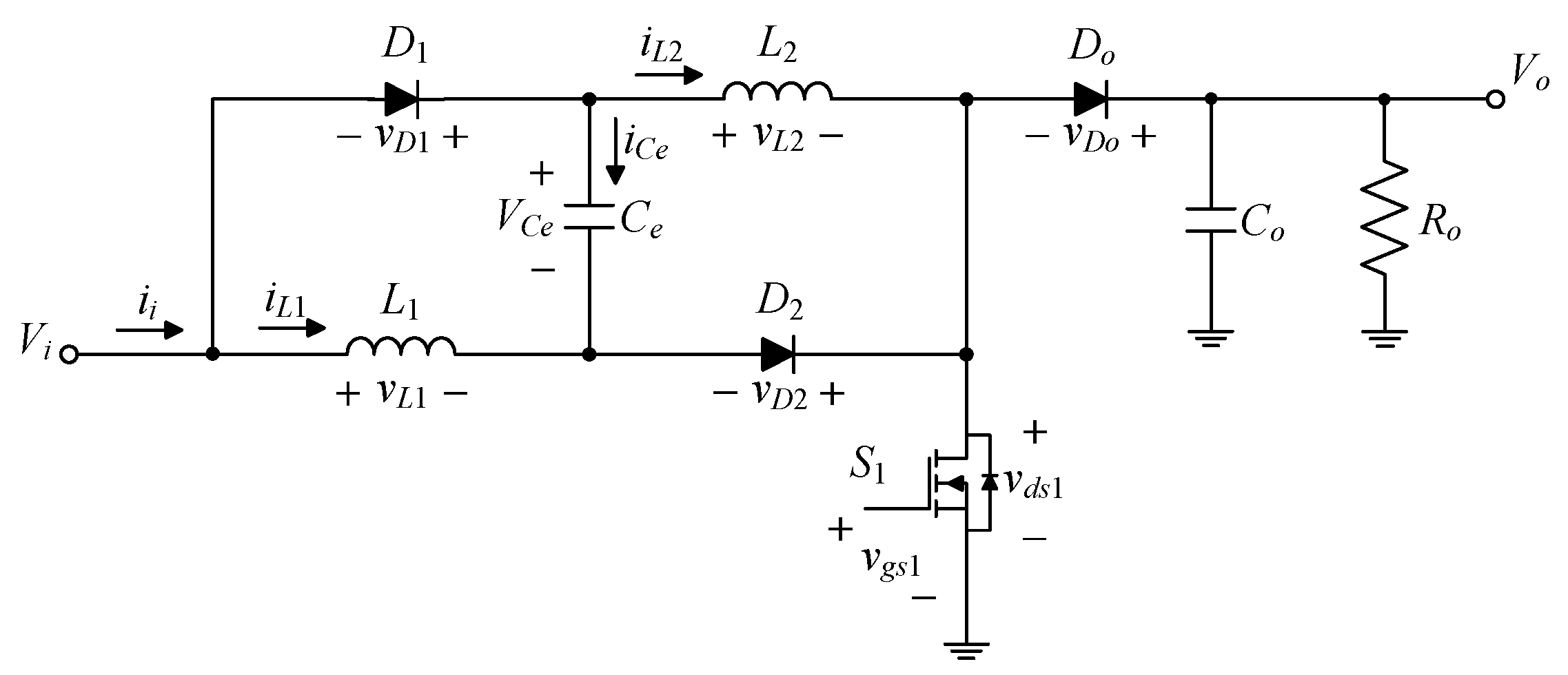
Figure 2.
Proposed charge-pump capacitor-based dual-boost inductor converter.
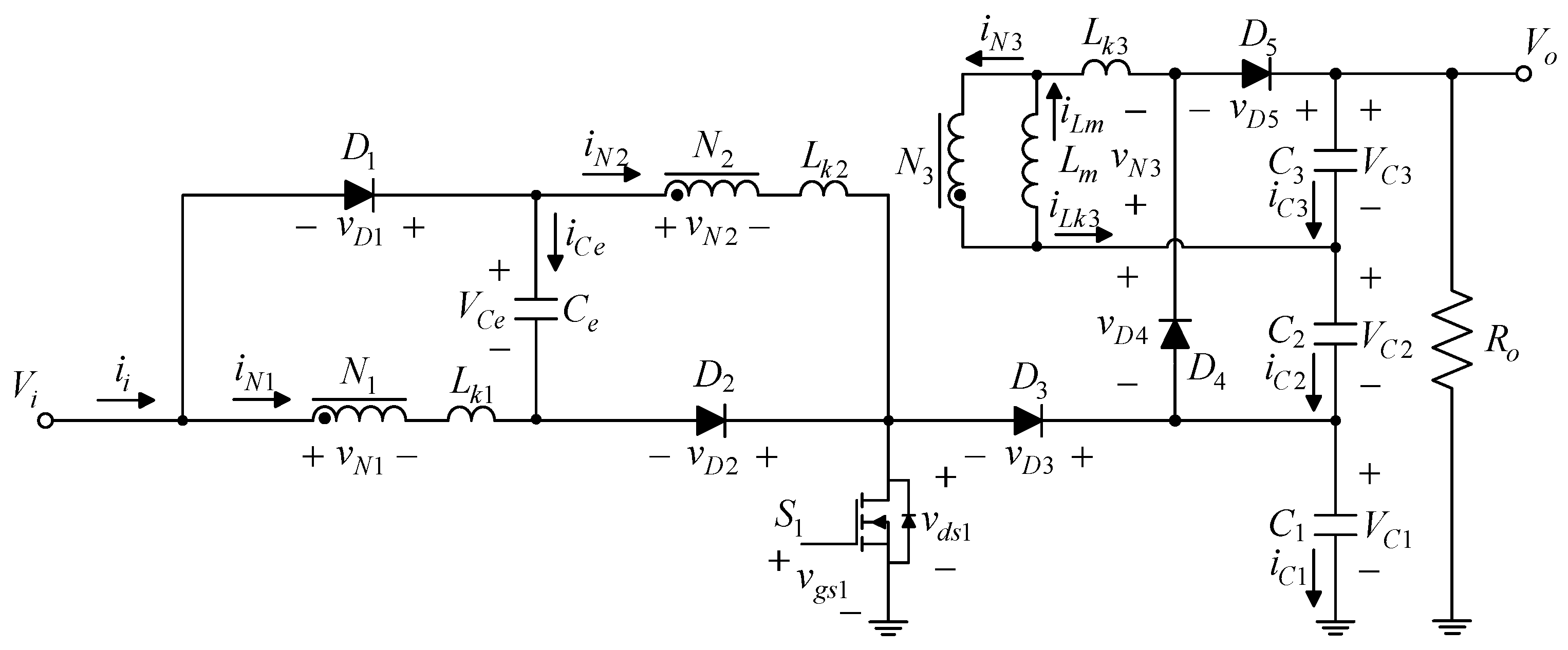
Figure 3.
Illustrated waveforms relevant to the proposed converter operation.
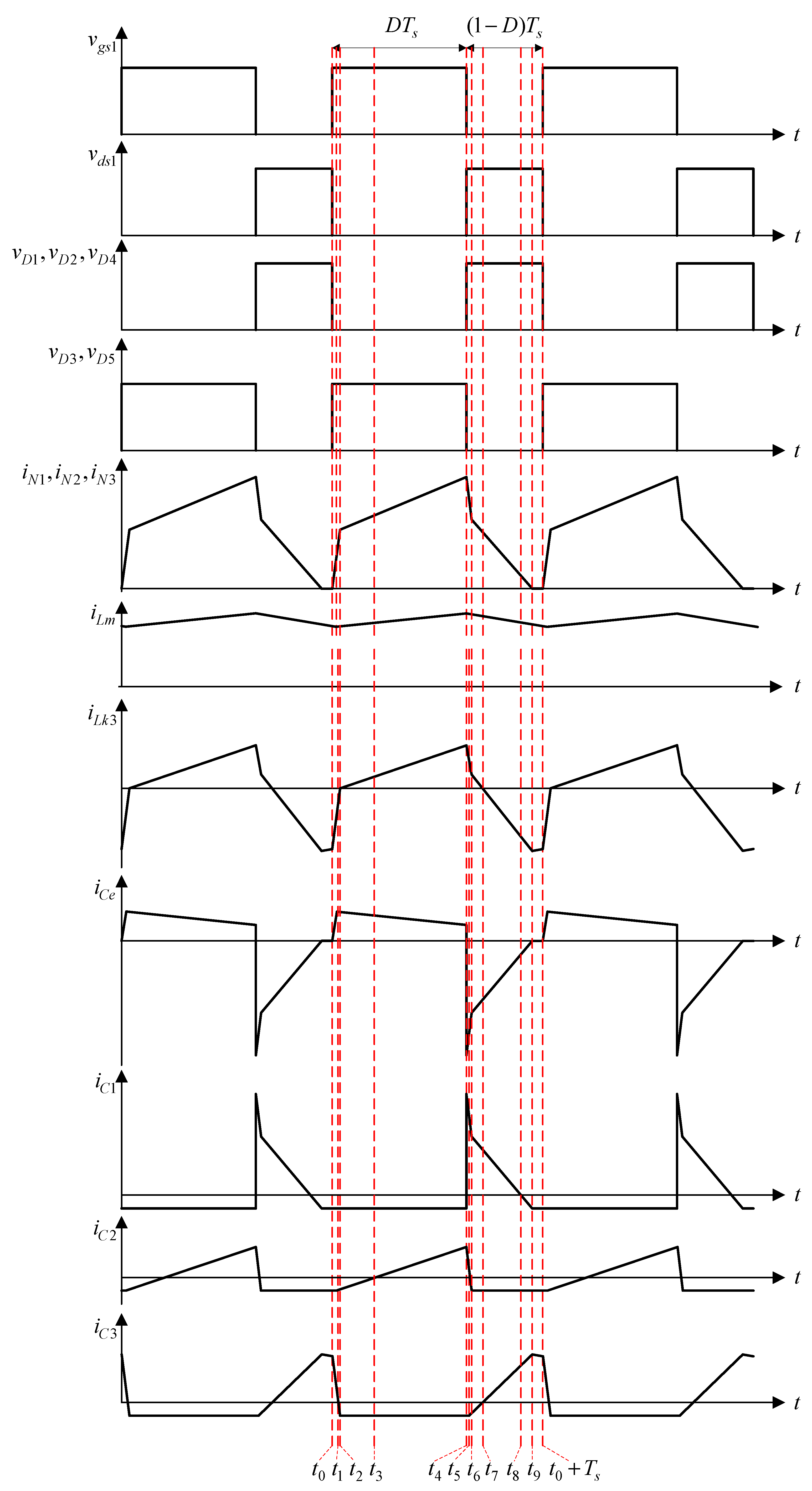
Figure 4.
Current flow in state 1.

Figure 5.
Current flow in state 2.
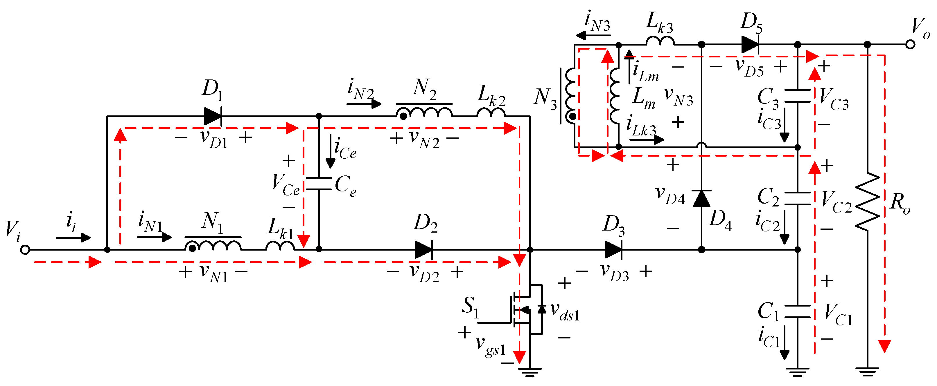
Figure 6.
Current flow in state 3.

Figure 7.
Current flow in state 4.
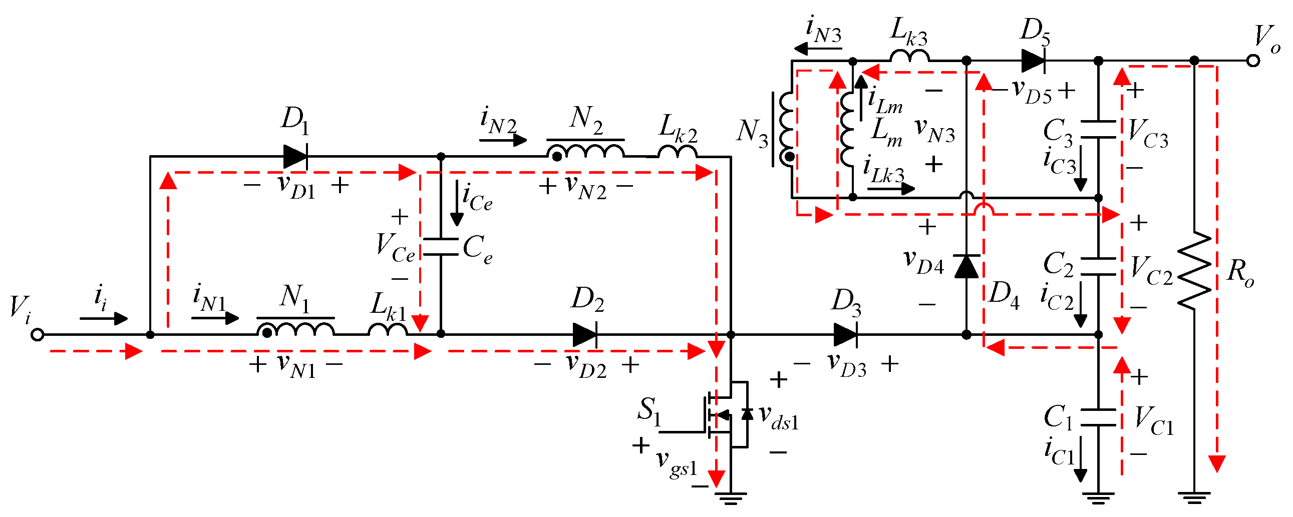
Figure 8.
Current flow in state 5.

Figure 9.
Current flow in state 6.
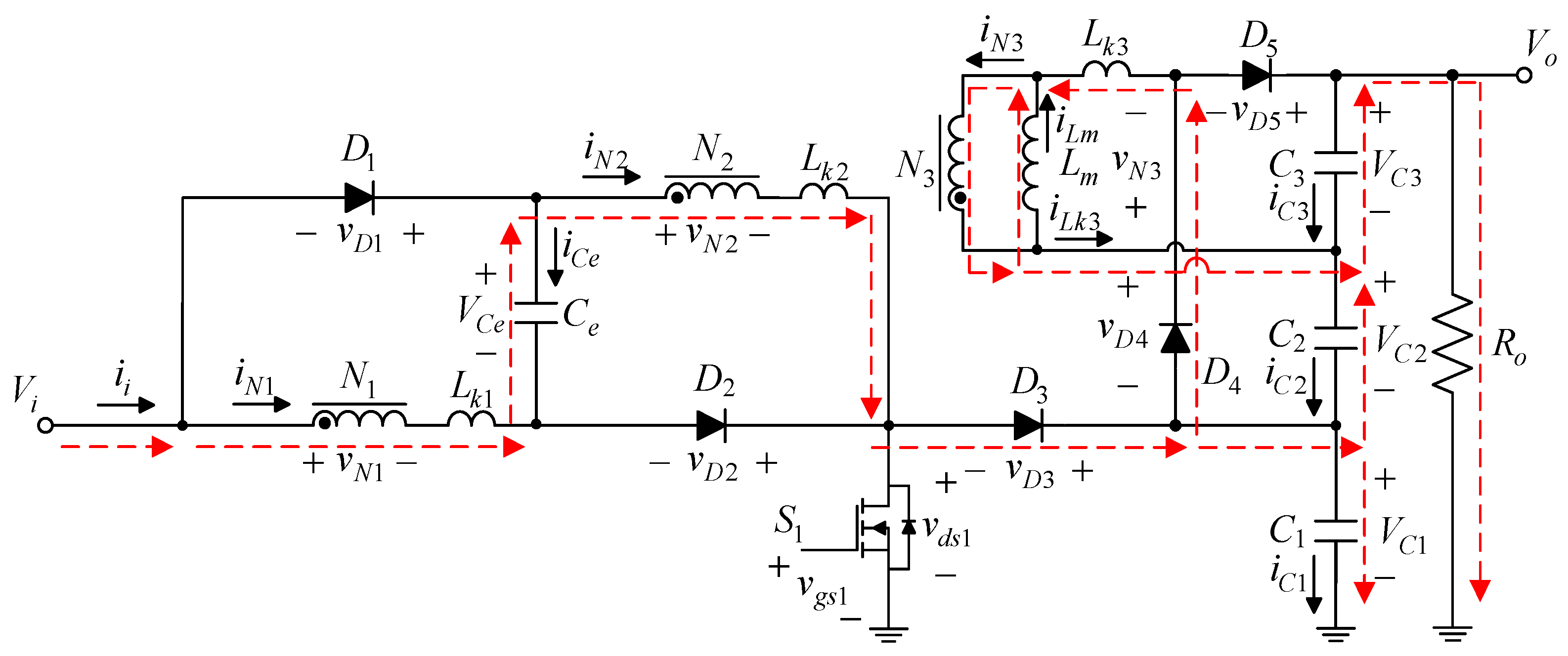
Figure 10.
Current flow in state 8.
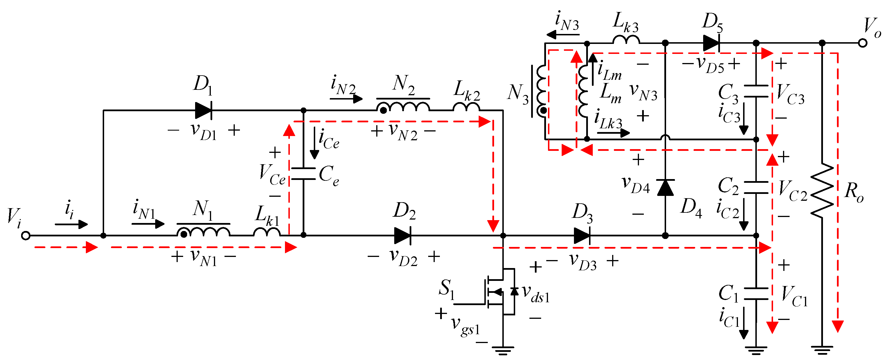
Figure 11.
Current flow in state 9.
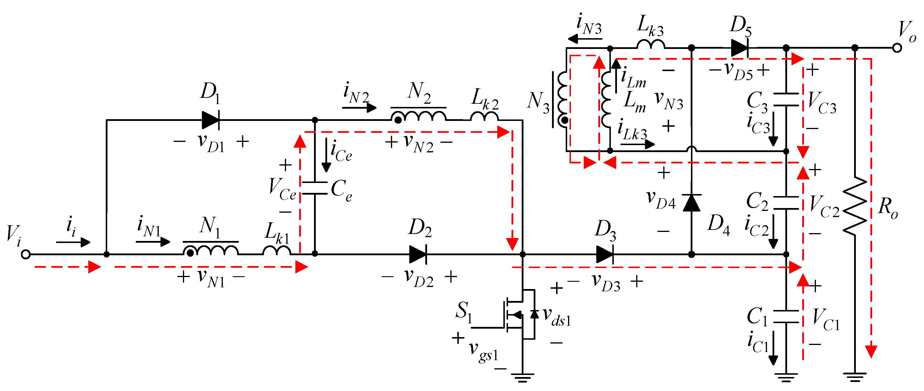
Figure 12.
Current flow in state 10.
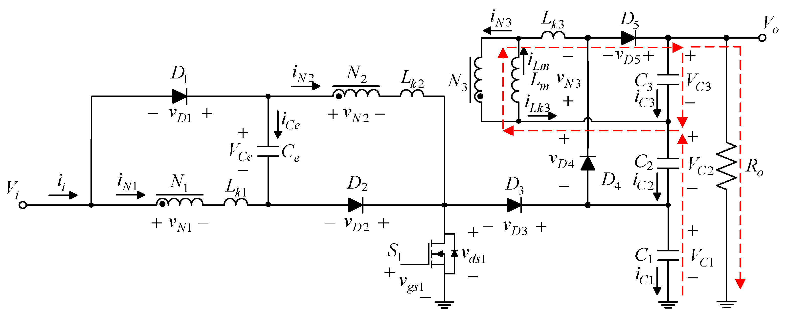
Figure 13.
Boundary curve between operating modes of Lm.
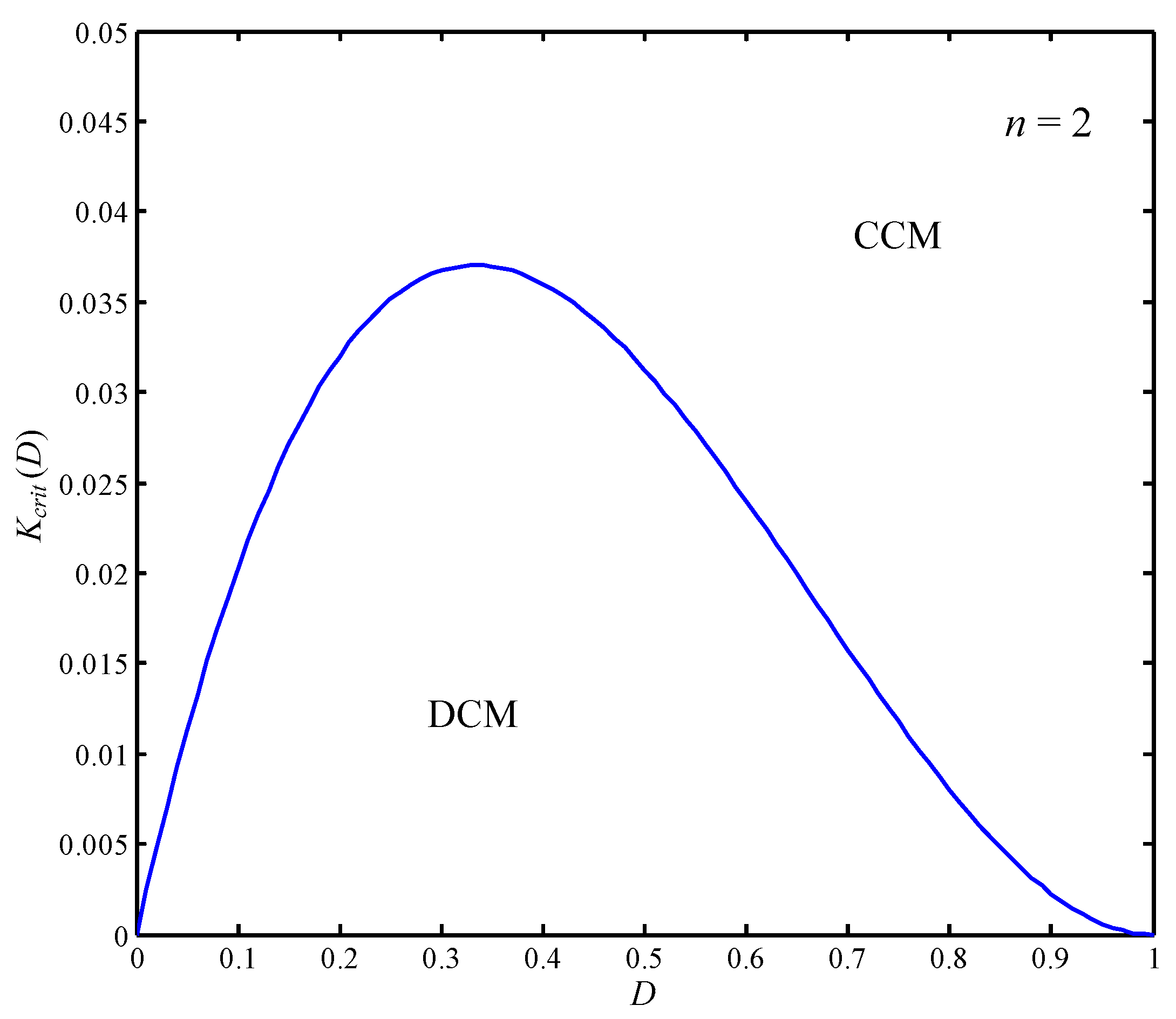
Figure 14.
System configuration of the proposed converter.
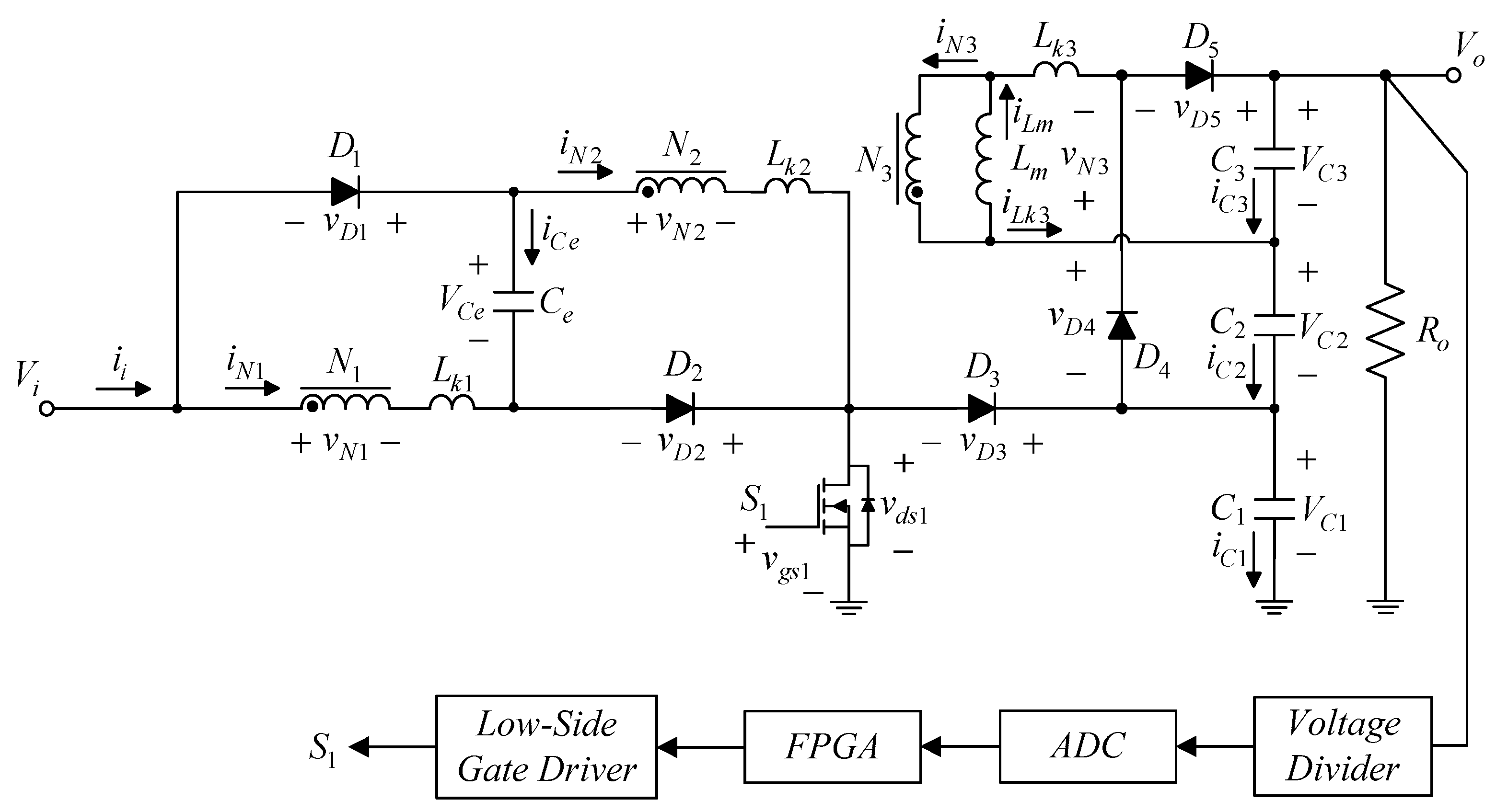
Figure 15.
Simulated circuit of the proposed converter.
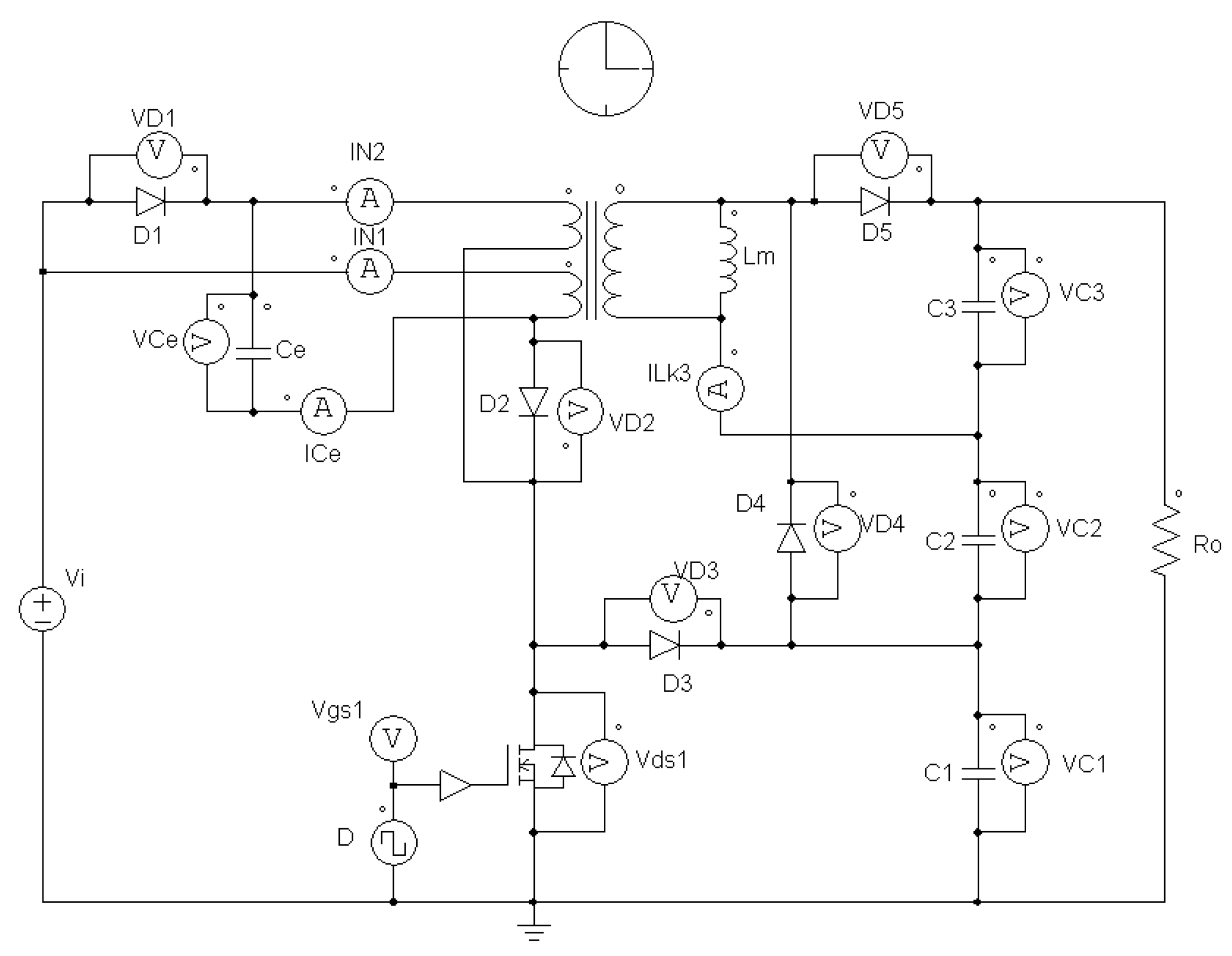
Figure 16.
Simulated waveforms at rated load: (1) ; (2) ; (3) ; (4) .

Figure 17.
Simulated waveforms at rated load: (1) ; (2) ; (3) ; (4) .
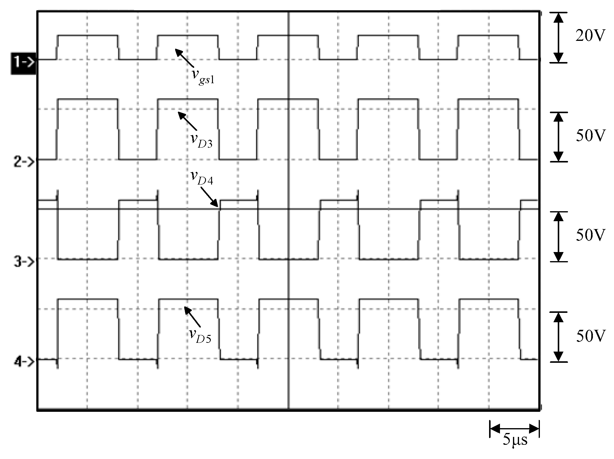
Figure 18.
Simulated waveforms at rated load: (1) ; (2) ; (3) ; (4) .
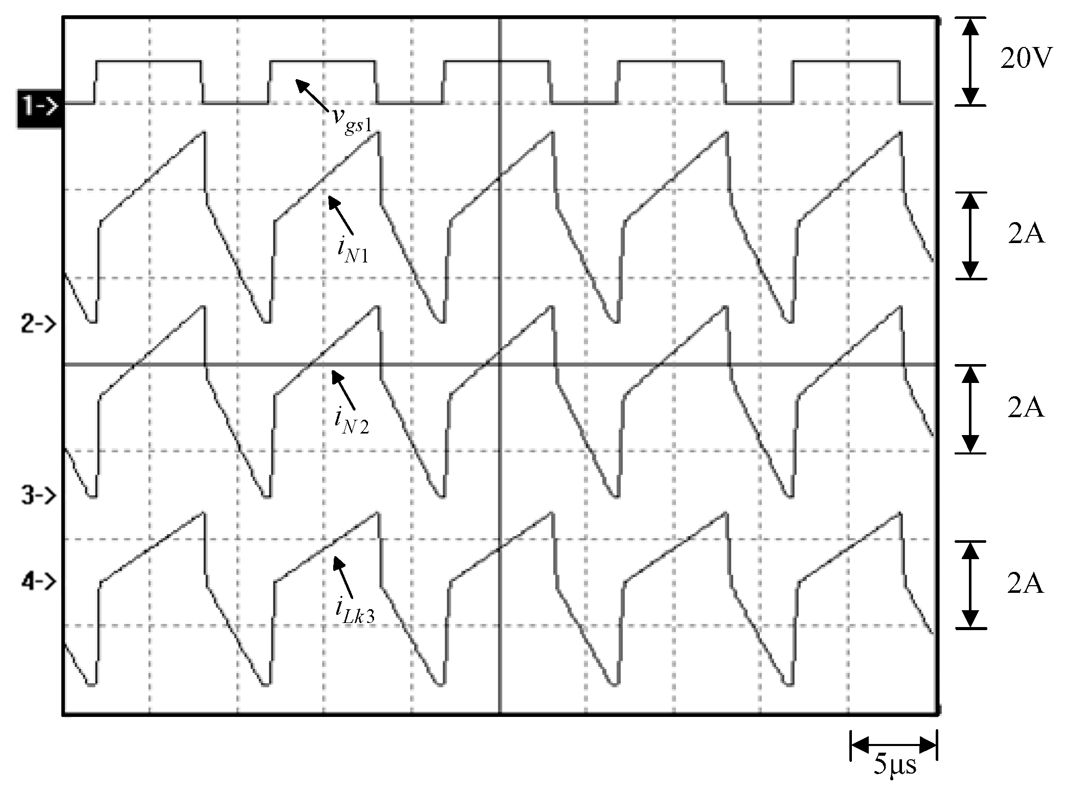
Figure 19.
Simulated waveforms at rated load: (1) ; (2) ; (3) .
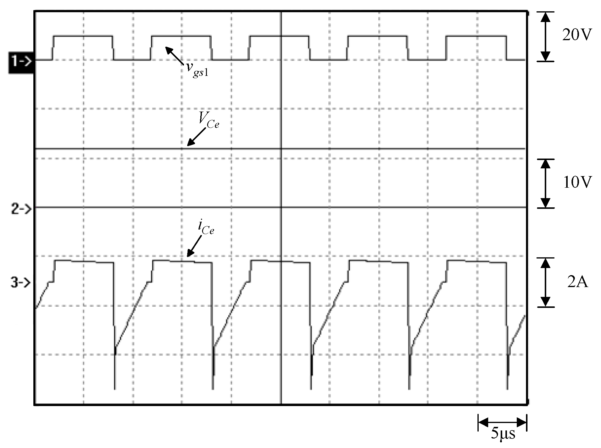
Figure 20.
Simulated waveforms at rated load: (1) ; (2) ; (3) ; (4) .

Figure 21.
Measured waveforms at minimum load: (1) ; (2) ; (3) ; () .

Figure 22.
Measured waveforms at minimum load: (1) ; (2) ; (3) ; (4) .
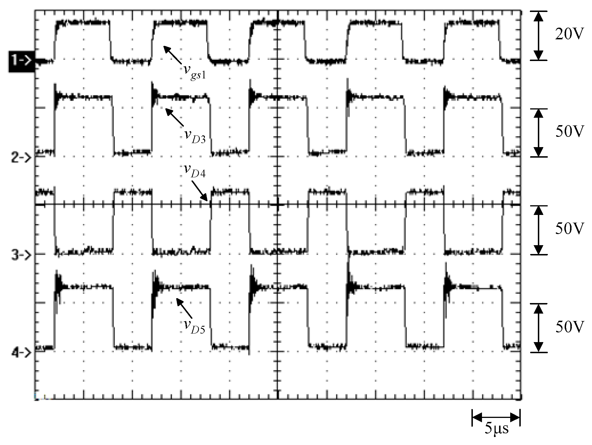
Figure 23.
Measured waveforms at minimum load: (1) ; (2) ; (3) ; (4) .
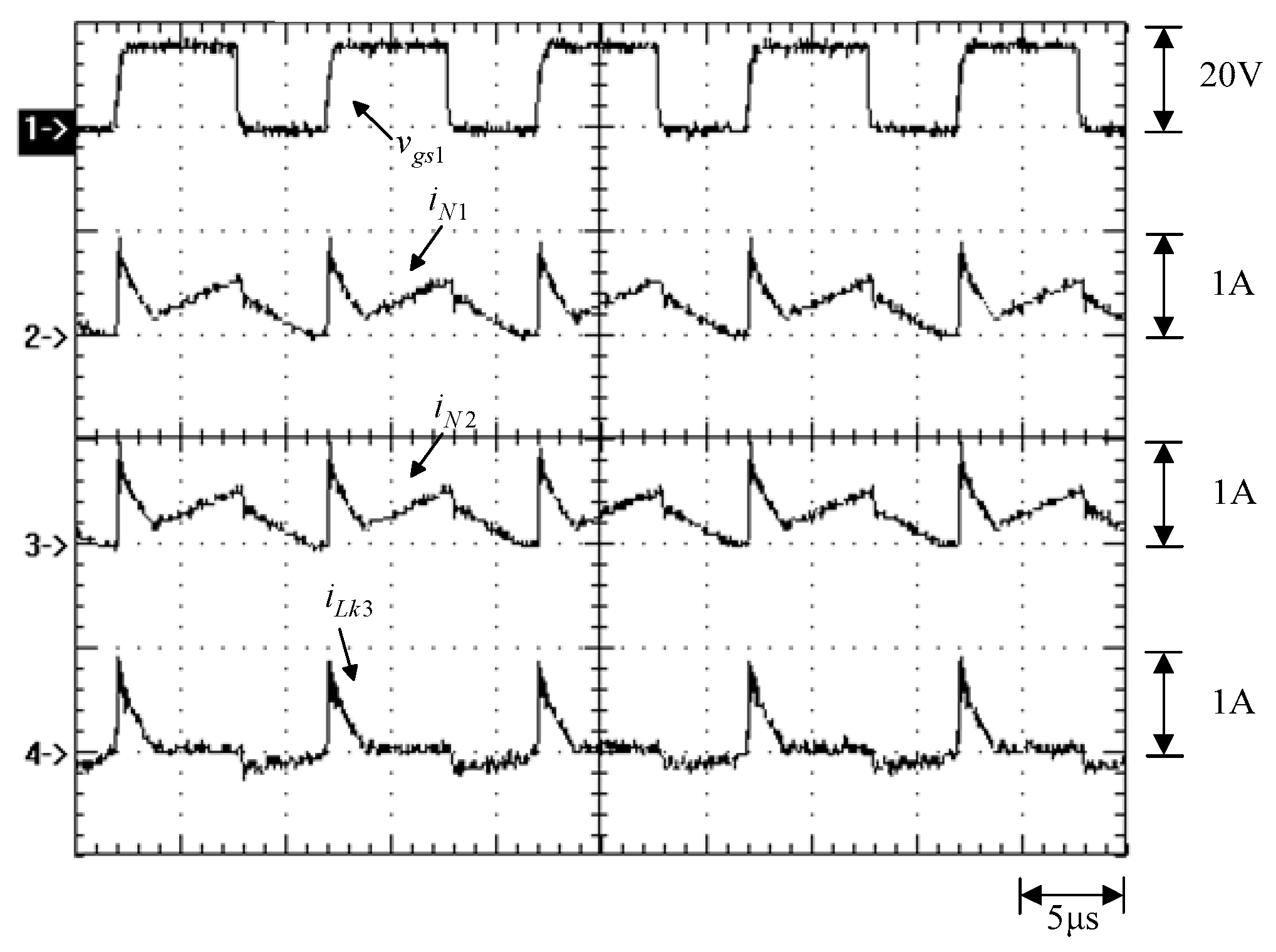
Figure 24.
Measured waveforms at minimum load: (1) ; (2) ; (3) .

Figure 25.
Measured waveforms at minimum load: (1) ; (2) ; (3) ; (4) .
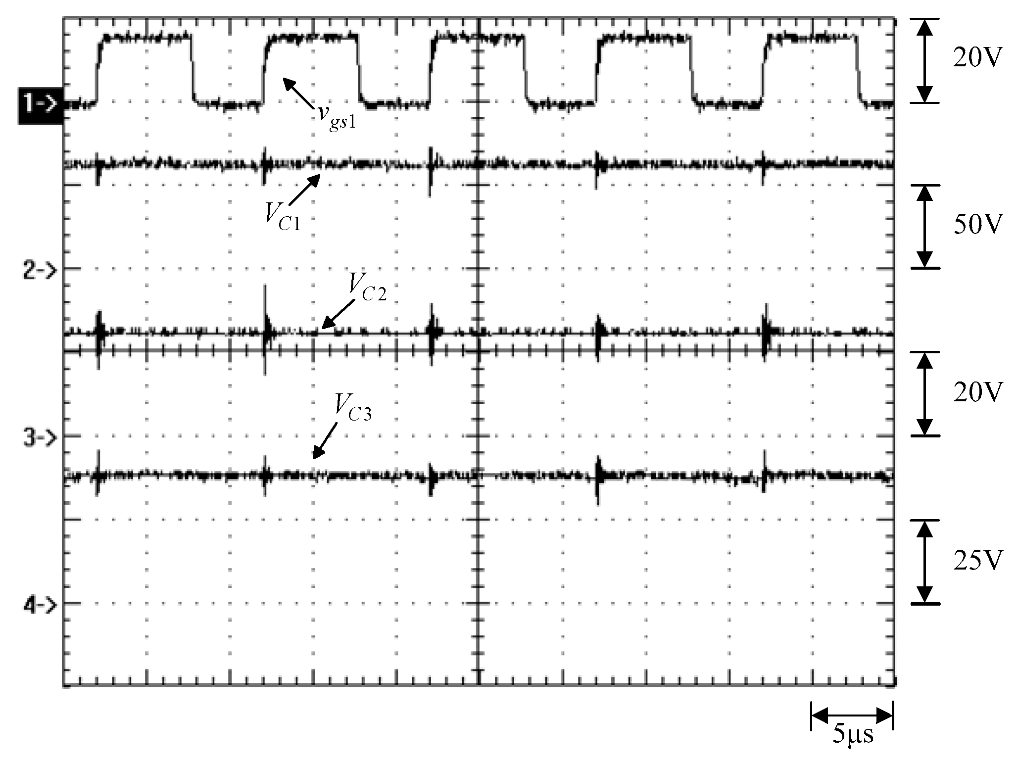
Figure 26.
Measured waveforms at half load: (1) ; (2) ; (3) ; () .
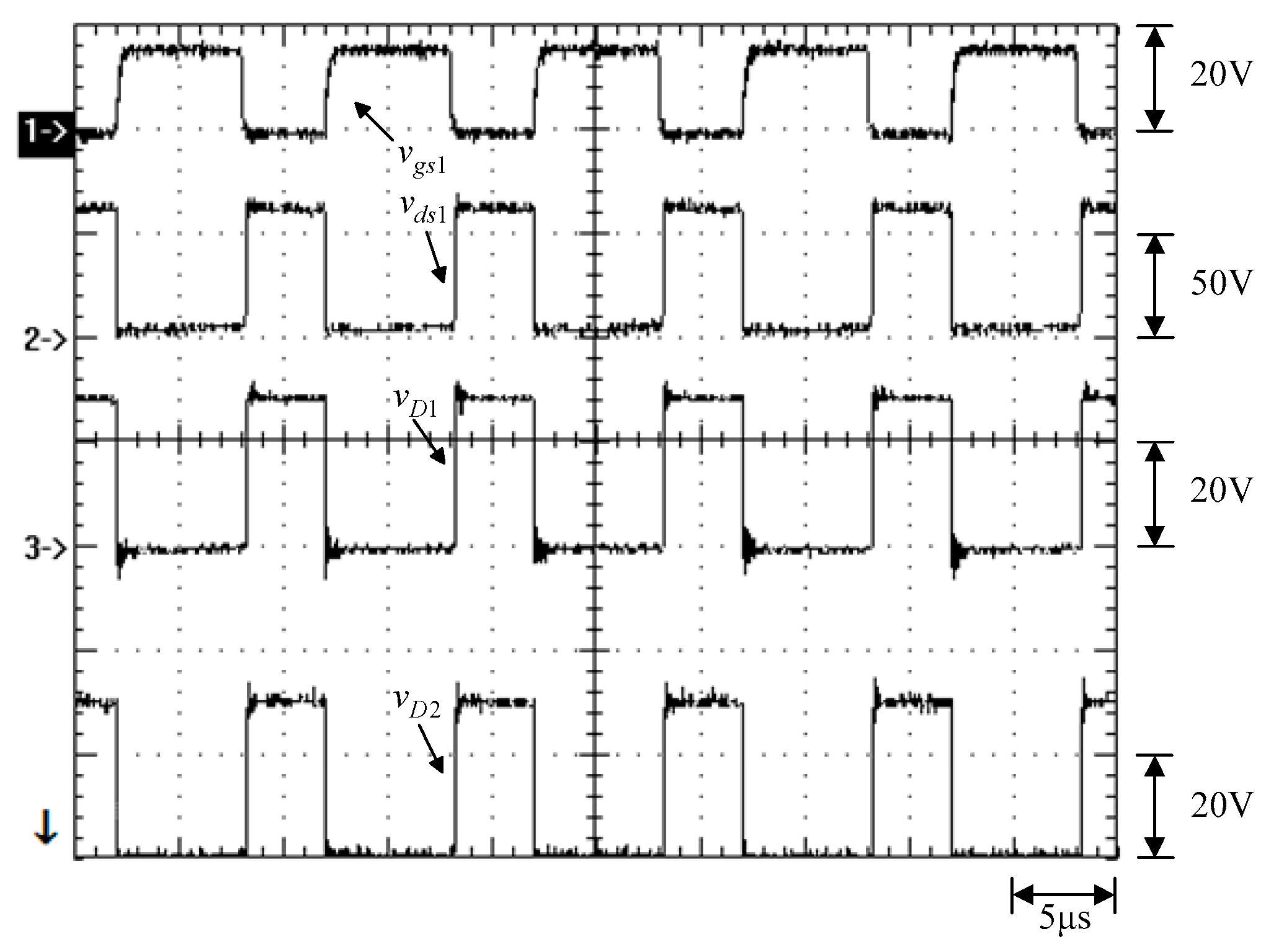
Figure 27.
Measured waveforms at half load: (1) ; (2) ; (3) ; (4) .
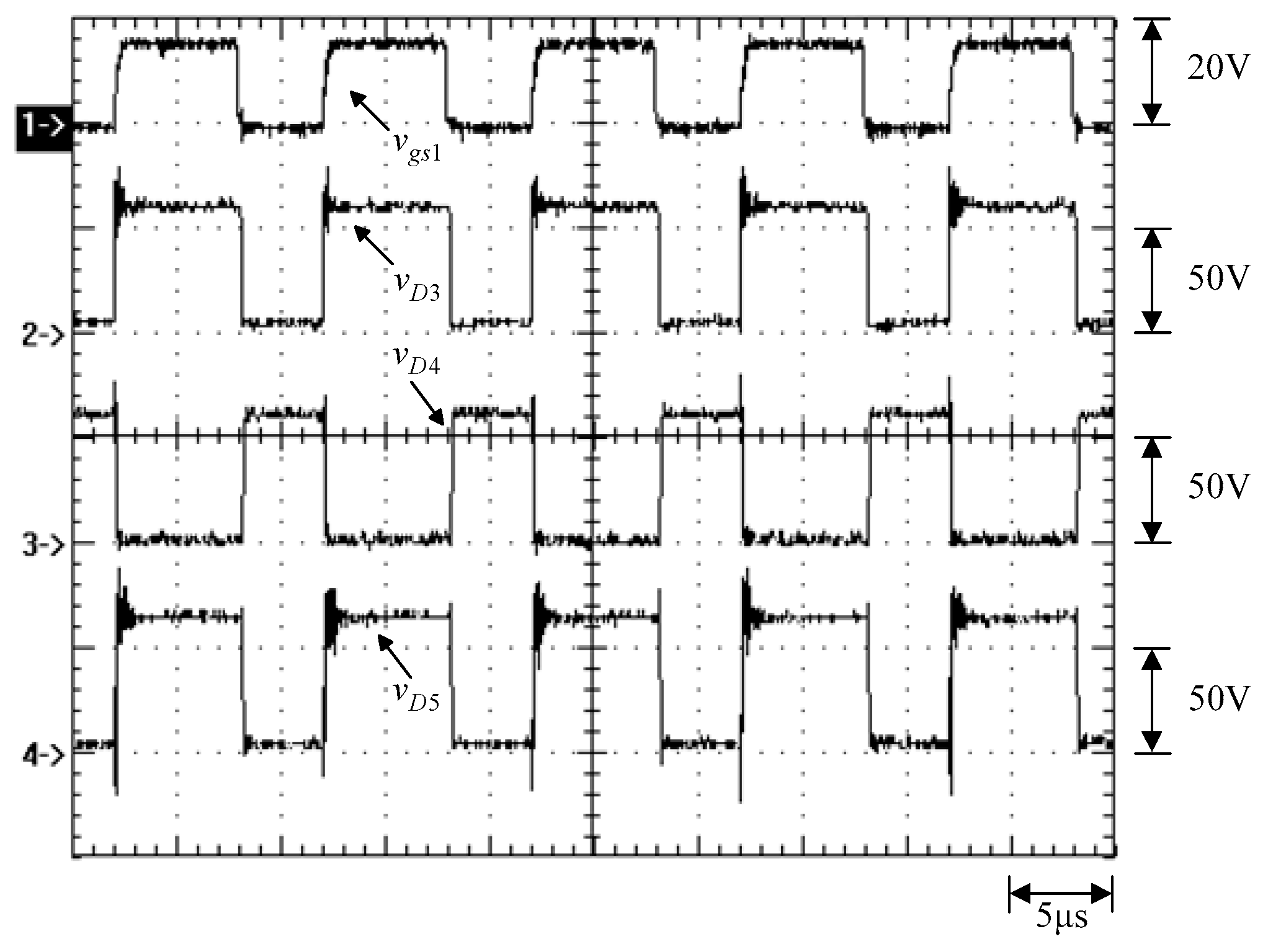
Figure 28.
Measured waveforms at half load: (1) ; (2) ; (3) ; (4) .
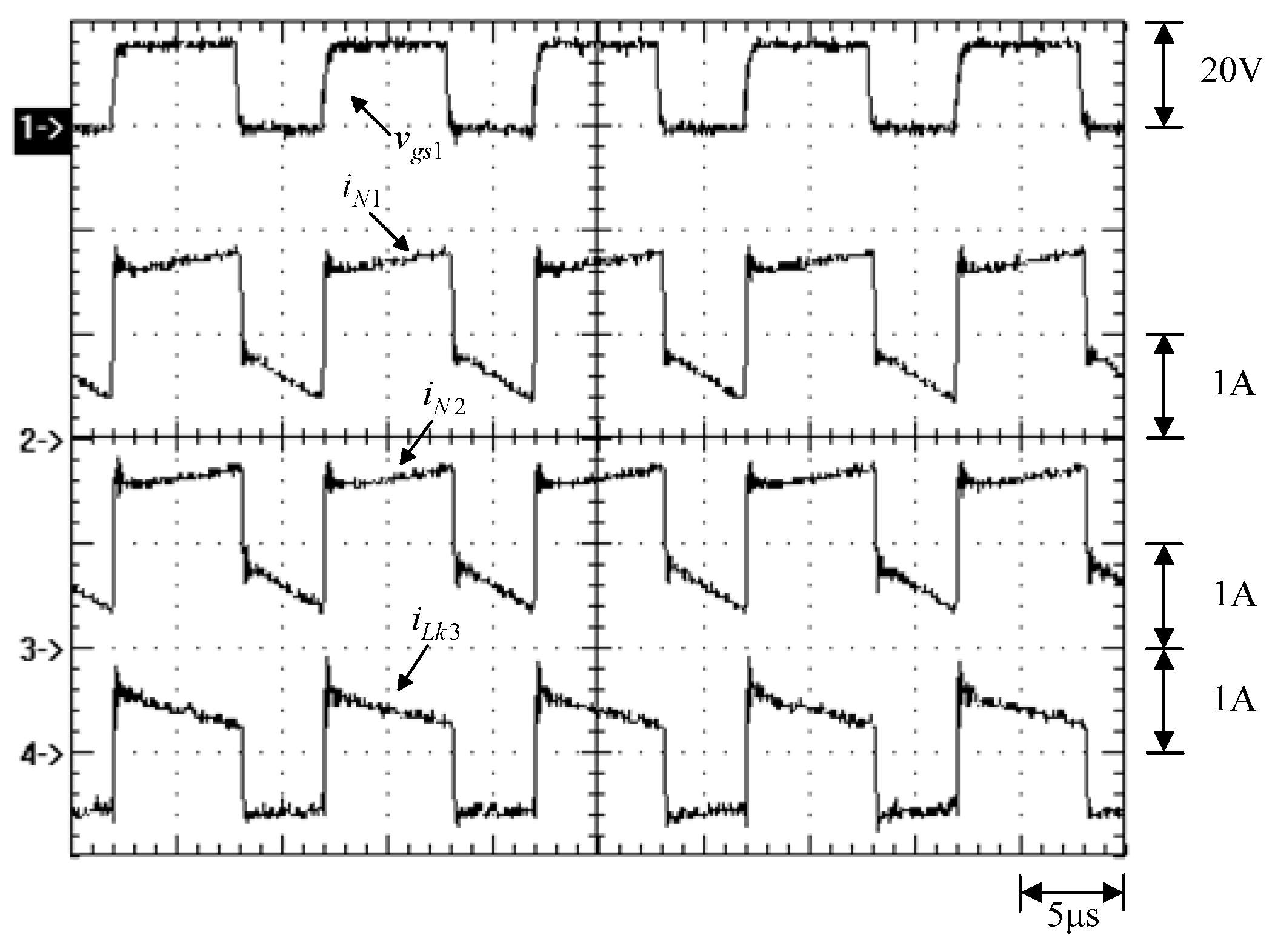
Figure 29.
Measured waveforms at half load: (1) ; (2) ; (3) .
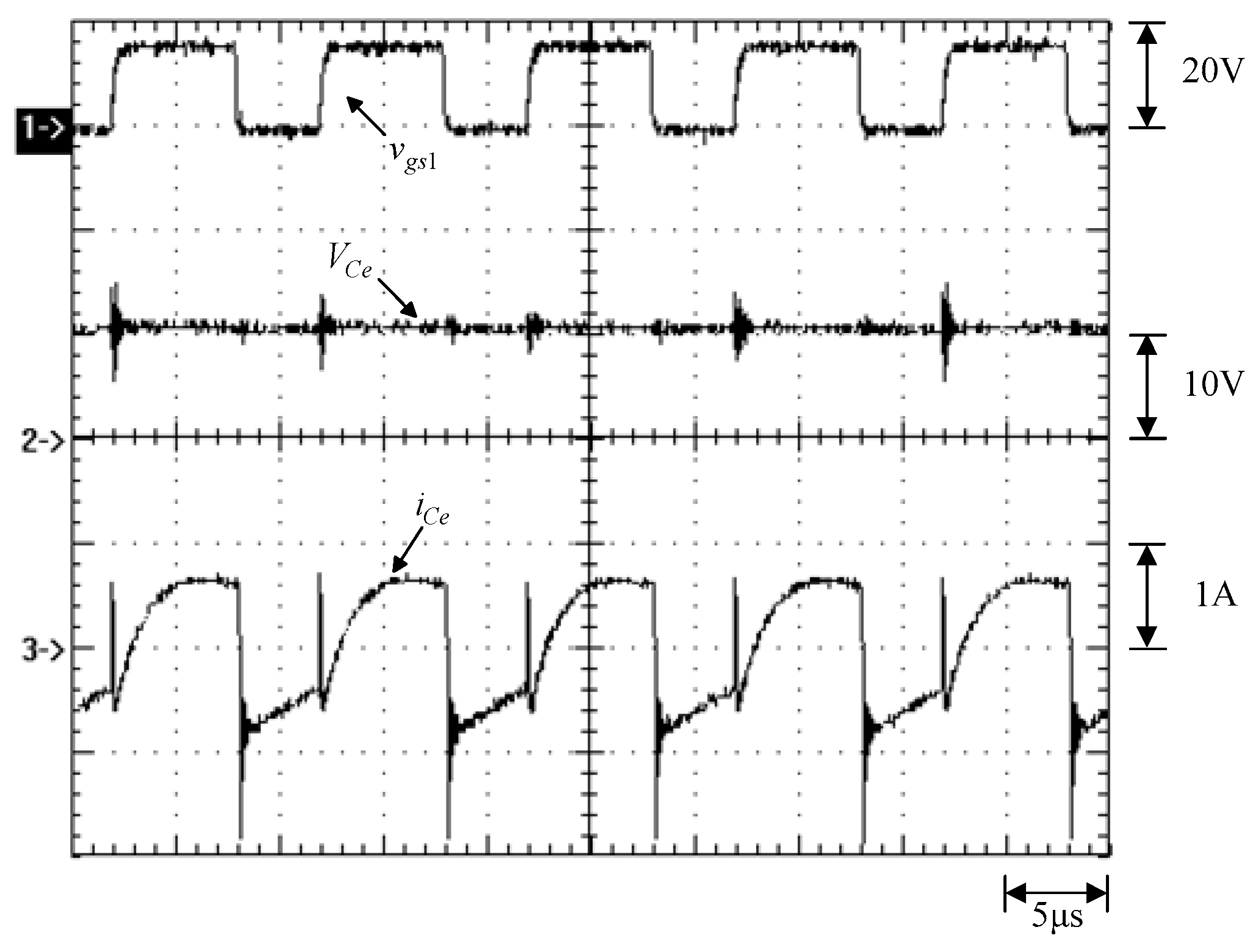
Figure 30.
Measured waveforms at half load: (1) ; (2) ; (3) ; (4) .
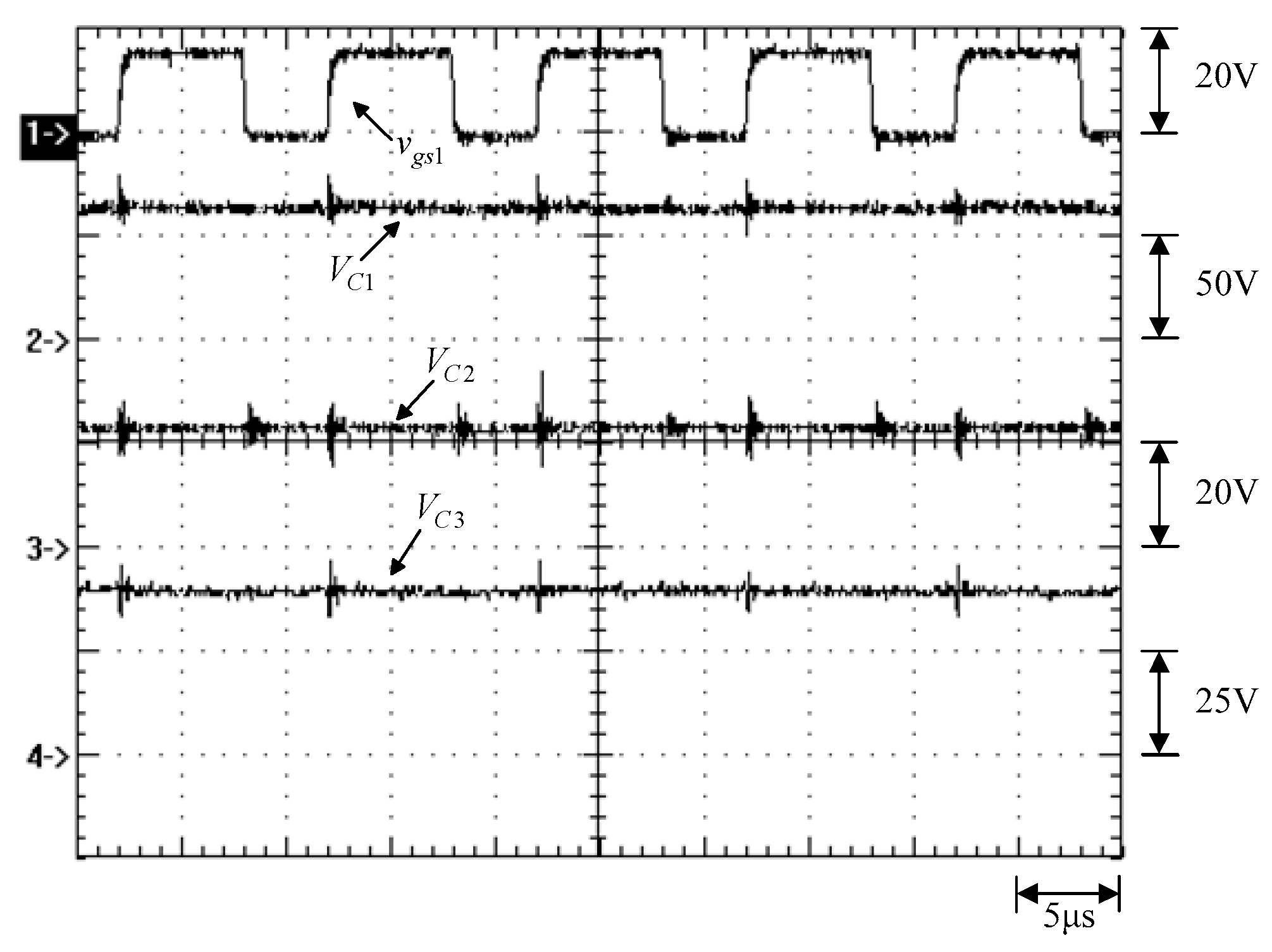
Figure 31.
Measured waveforms at rated load: (1) ; (2) ; (3) ; () .

Figure 32.
Measured waveforms at rated load: (1) ; (2) ; (3) ; (4) .
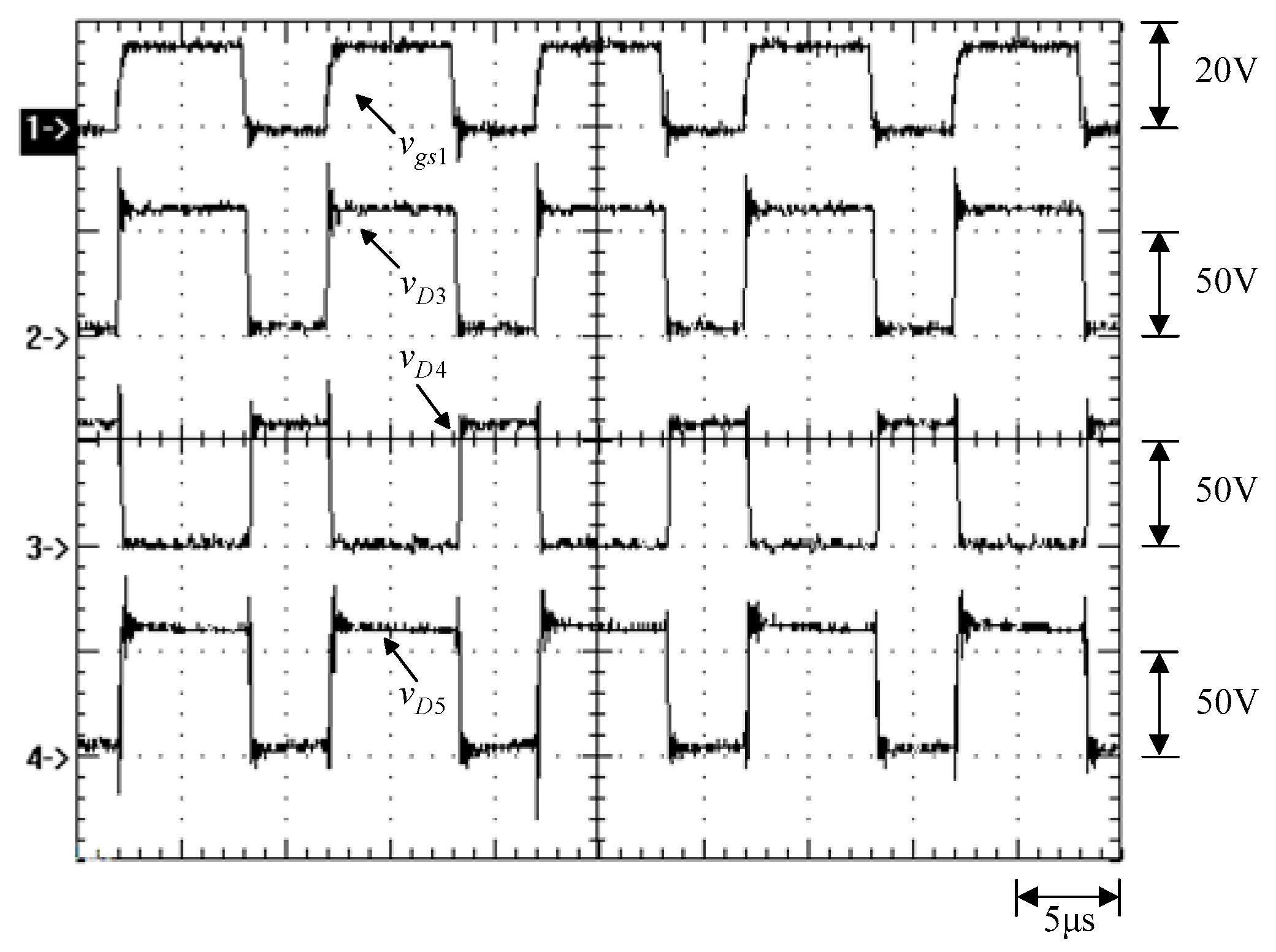
Figure 33.
Measured waveforms at rated load: (1) ; (2) ; (3) ; (4) .

Figure 34.
Measured waveforms at rated load: (1) ; (2) ; (3) .

Figure 35.
Measured waveforms at rated load: (1) ; (2) ; (3) ; (4) .
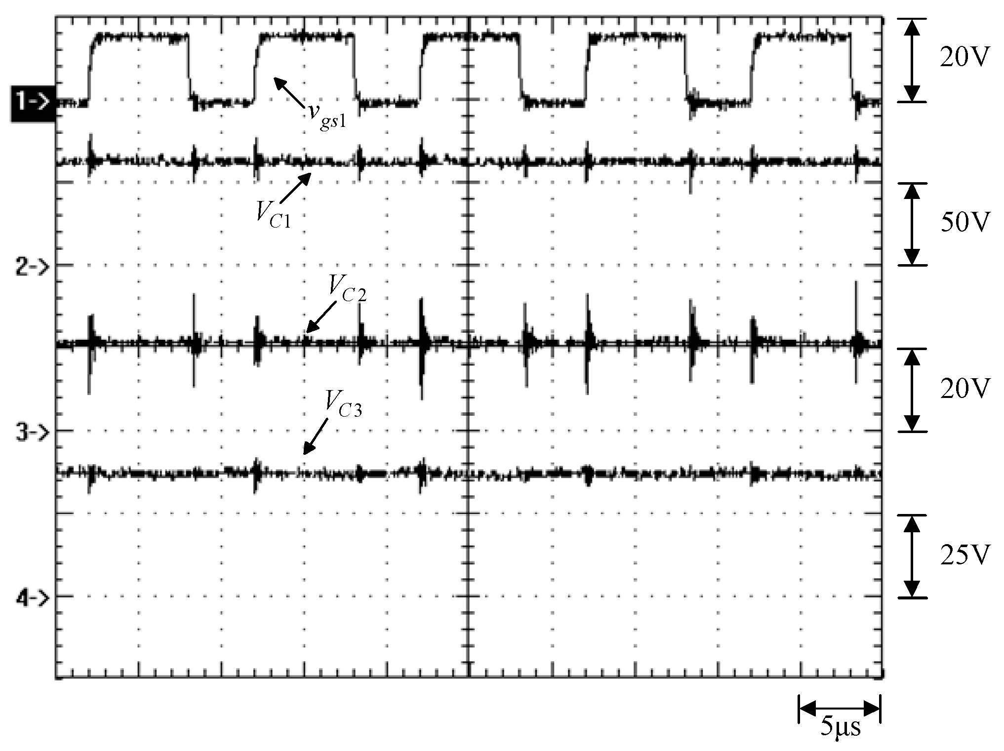
Figure 36.
Load transient response from minimum load to half load.
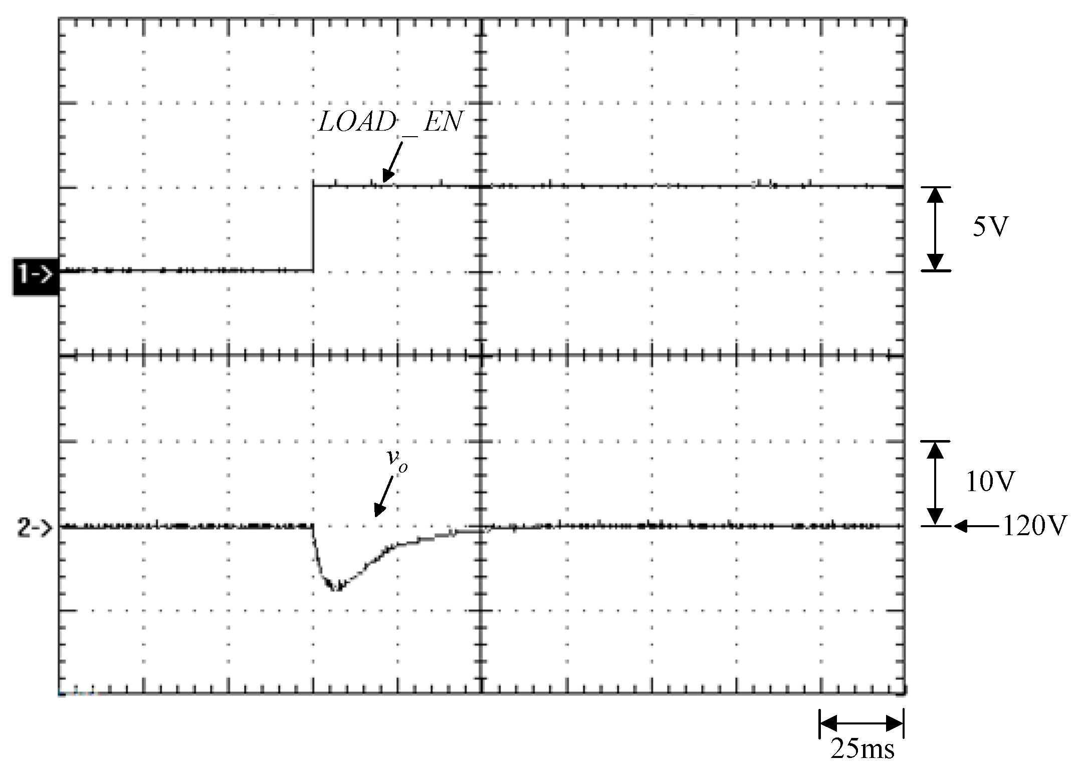
Figure 37.
Load transient response from half load to minimum load.
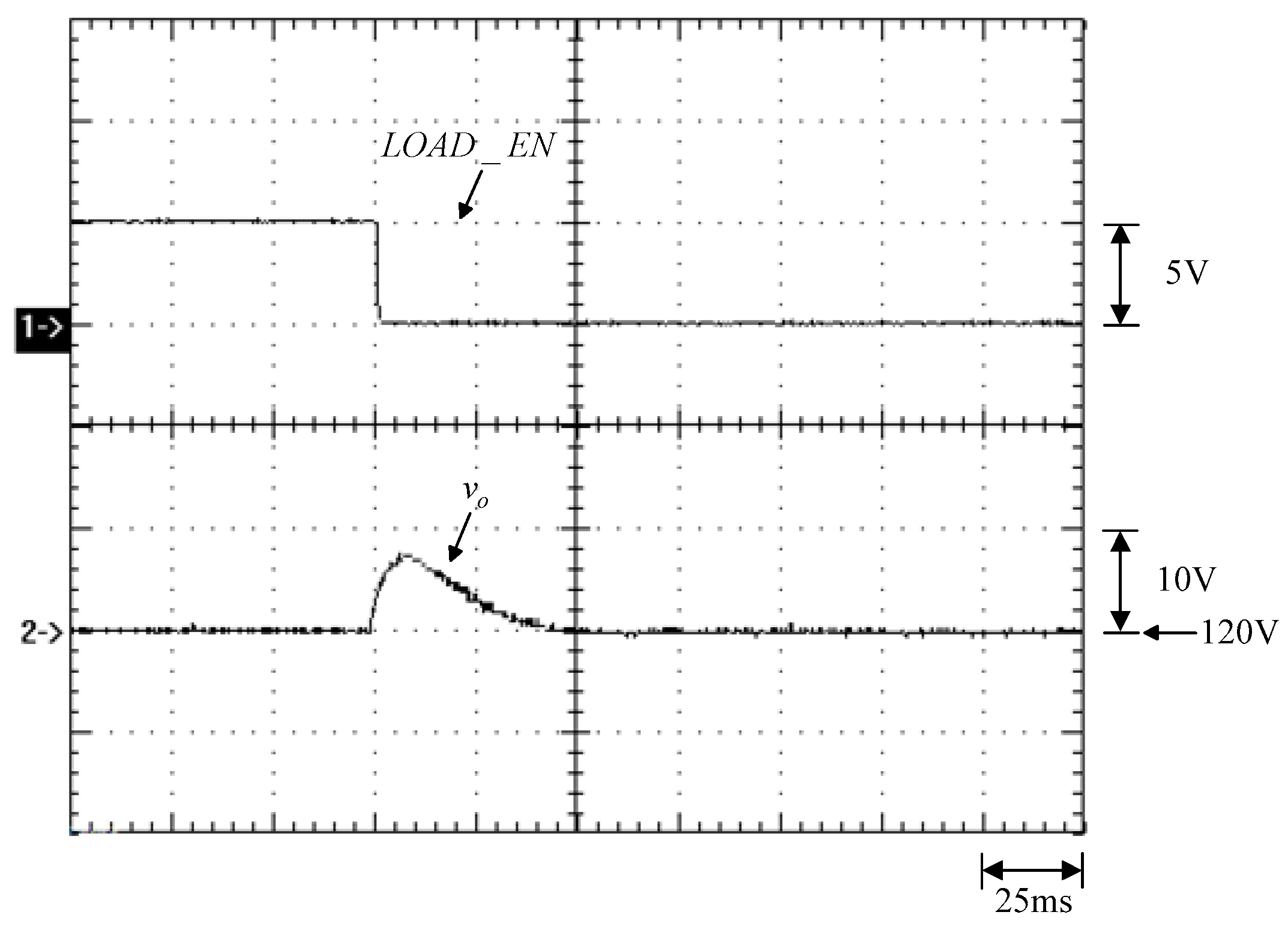
Figure 38.
Load transient response from half load to rated load.
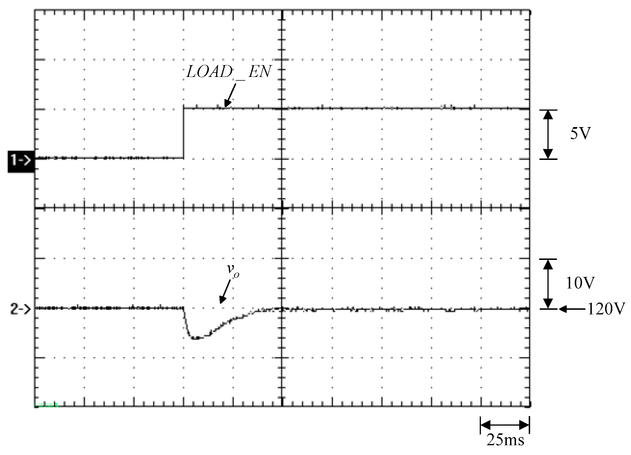
Figure 39.
Load transient response from rated load to half load.
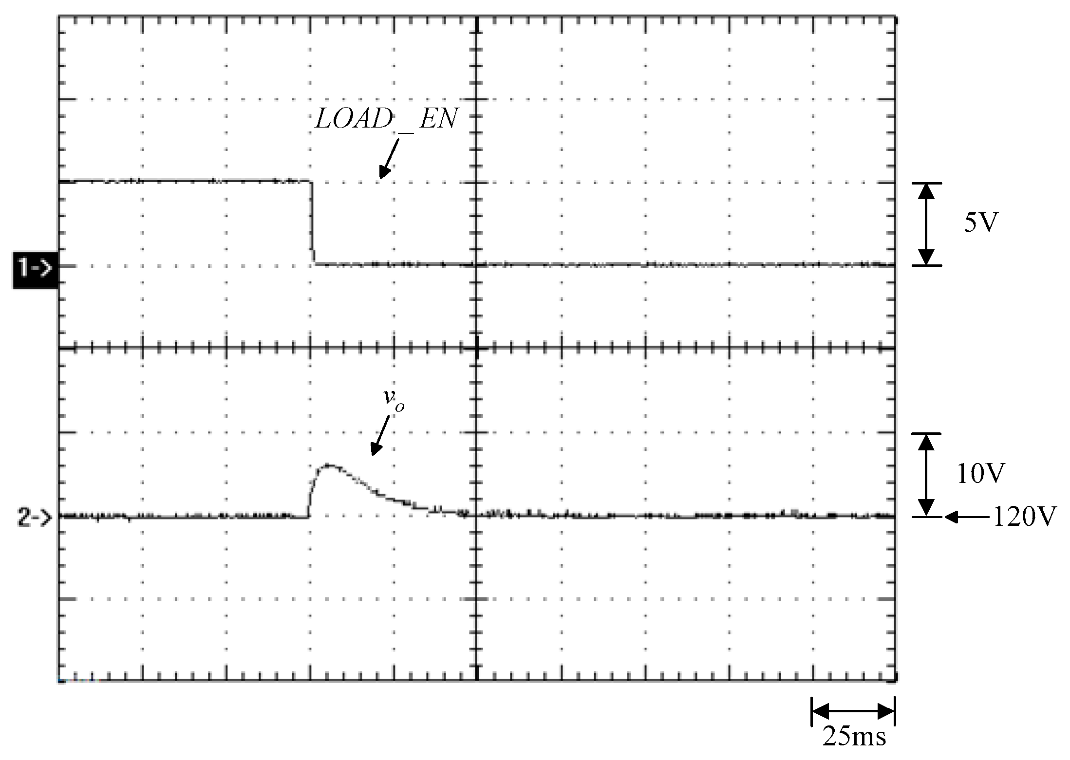
Figure 40.
Load transient response from minimum load to rated load.
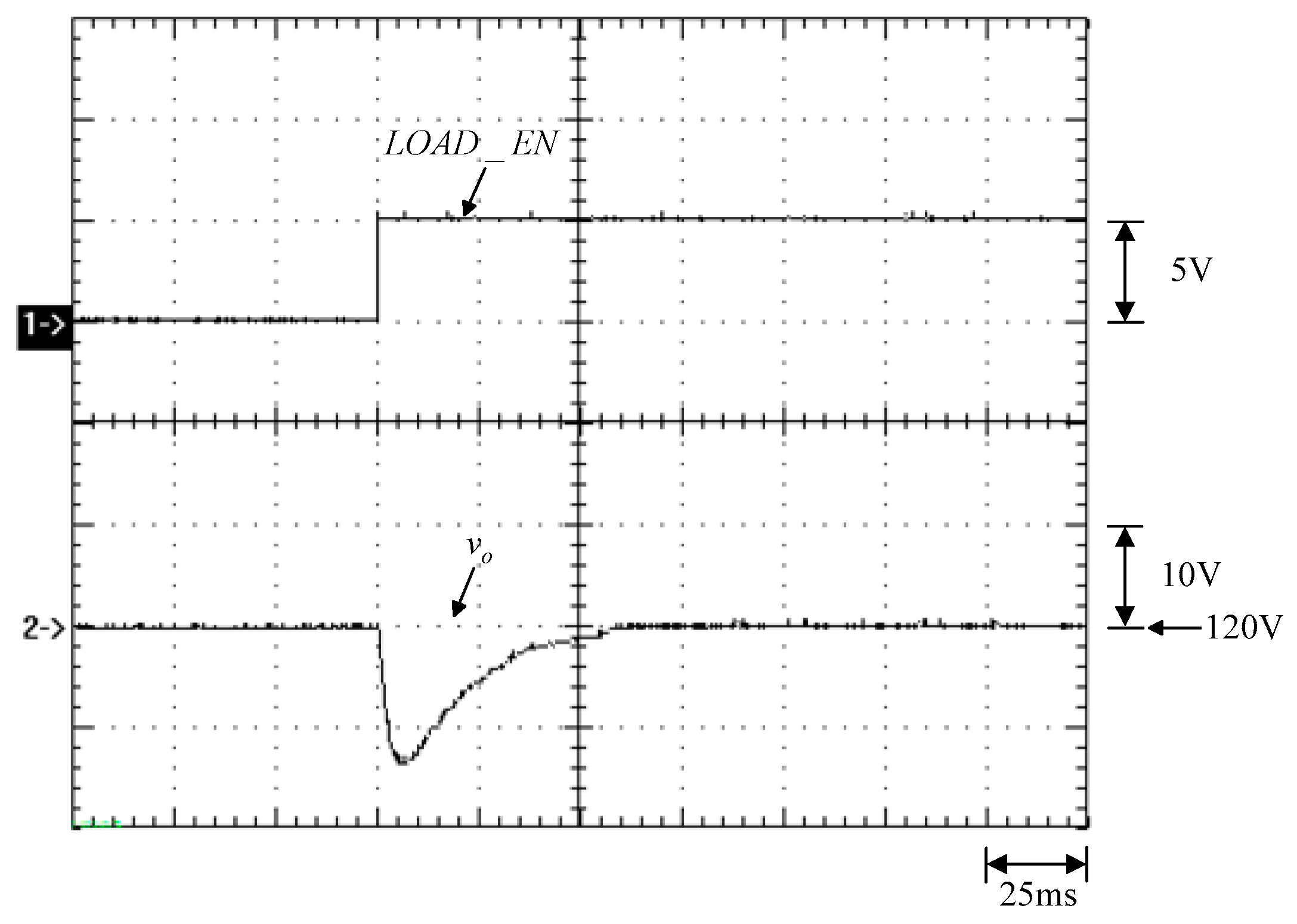
Figure 41.
Load transient response from rated load to minimum load.

Figure 42.
Efficiency measurement block diagram.

Figure 43.
Curve of efficiency versus load current.

Figure 44.
Photo of the experimental setup.

Table 1.
Component specifications.
| Component | Specification |
|---|---|
| Switch S1 | STP120NF10 |
| Diodes D1, D2 | MBRH2060CT |
| Diodes D3, D4, D5 | V20120C |
| Energy-Transferring Capacitor Ce | Ce = 470 µF/50 V Rubycon |
| Output Capacitors C1, C2, C3 | C1 = 100 µF/100 V Rubycon C2 = C3 = 50 µF/100 V Rubycon |
| Coupled Inductor | PC44PQ26/25Z-12 Lm = 300 µH N1 = N2 = 11 turns, N3 = 22 turns Lk1 = Lk2 = 180 nH, Lk3 = 90 nH |
| Gate Driver | TC4420 |
| FPGA | Cyclone I |
Table 2.
Comparison of the existing and proposed converters.
| Reference Number | CCM Voltage Gain | Total Component No. | Diode No. | Switch No. | Inductor No. | Capacitor No. | Switching Frequency | Efficiency |
|---|---|---|---|---|---|---|---|---|
| [18] | 14 | 4 | 1 | 4 | 1 | 55 kHz | 94.40% | |
| [19] | 16 | 5 | 1 | 4 | 6 | 60 kHz | 95.10% | |
| [20] | 16 | 6 | 1 | 4 | 5 | 50 kHz | 94.70% | |
| [21] | 16 | 5 | 2 | 3 | 6 | 33 kHz | 95.22% | |
| [22] | 8 | 3 | 1 | 2 | 2 | 100 kHz | 92.50% | |
| Proposed | 13 | 5 | 1 | 1 | 4 | 100 kHz | 92.61% |
Disclaimer/Publisher’s Note: The statements, opinions and data contained in all publications are solely those of the individual author(s) and contributor(s) and not of MDPI and/or the editor(s). MDPI and/or the editor(s) disclaim responsibility for any injury to people or property resulting from any ideas, methods, instructions or products referred to in the content. |
© 2023 by the authors. Licensee MDPI, Basel, Switzerland. This article is an open access article distributed under the terms and conditions of the Creative Commons Attribution (CC BY) license (https://creativecommons.org/licenses/by/4.0/).
Share and Cite
MDPI and ACS Style
Hwu, K.-I.; Tseng, P.-C. High Step-Up Converter. Electronics 2023, 12, 4000. https://doi.org/10.3390/electronics12194000
AMA Style
Hwu K-I, Tseng P-C. High Step-Up Converter. Electronics. 2023; 12(19):4000. https://doi.org/10.3390/electronics12194000
Chicago/Turabian StyleHwu, Kuo-Ing, and Pei-Ching Tseng. 2023. "High Step-Up Converter" Electronics 12, no. 19: 4000. https://doi.org/10.3390/electronics12194000
Note that from the first issue of 2016, this journal uses article numbers instead of page numbers. See further details here.