Article

A Wideband and Low Reference Spur PLL with Clock Feedthrough Suppressed and Low Current Mismatch Charge Pump and Symmetrical CML Divider

1
Institute of Microelectronics of the Chinese Academy of Sciences, Beijing 100029, China
2
School of Integrated Circuits, University of Chinese Academy of Sciences, Beijing 100049, China
3
State Key Lab of Fabrication Technologies for Integrated Circuits, Beijing 100029, China
*
Author to whom correspondence should be addressed.
Electronics 2023, 12(19), 4164; https://doi.org/10.3390/electronics12194164
Submission received: 12 September 2023 / Revised: 4 October 2023 / Accepted: 5 October 2023 / Published: 7 October 2023

Abstract

:
This paper presents the design and performance analysis of a wideband charge-pump phase-locked loop (CPPLL) characterized by low reference spur and low phase noise. The proposed CPPLL, operating as a wideband phase-locked loop (PLL) with a reference frequency of 100 MHz, achieves a wide tuning range of 40% from 2.0 GHz to 3.0 GHz. A clock feedthrough suppressed charge pump with additional bias current branches is used to reduce the PLL’s loop reference spur. The 4-stage current mode logic (CML) divide-by-2/3 circuit is utilized in the frequency divider to achieve high-speed frequency division. The circuit of an AND gate and latch in the 2/3 divider adopts a full differential symmetric structure to minimize the phase error of high-frequency differential signals. The voltage-controlled oscillator (VCO) is designed to provide a wide tuning range while optimizing the trade-off between the phase noise and power consumption. The fabricated PLL is implemented using a 0.13 µm CMOS process. Experimental measurements reveal a reference spur of −74.39 dBc at an oscillation frequency of 2.4 GHz. Moreover, the CPPLL achieves phase noise of −102.55 dBc/Hz@100 kHz and −127.15 dBc/Hz@1 MHz, while consuming 33.6 mW under a 1.2 V supply voltage. The integrated root-mean-square (rms) jitter, measured from 10 kHz to 10 MHz, is 340.99 fs, and the figure-of-merit (FoM) is −234.08 dB at a carrier frequency of 2.4 GHz, highlighting the potential of the proposed PLL for integrated circuit applications.

1. Introduction

The phase-locked loop (PLL) is a ubiquitous component in wireless communication systems. It is responsible for generating the desired frequency signal for frequency down-conversion and up-conversion. With the increasing demand for high-speed and wideband communication systems, the design of PLLs with improved performance metrics has become crucial.
The performance concerning the reference spur is crucial for PLLs, as an inadequate reference spur can result in significant inter-channel crosstalk. Previous research in the field has primarily focused on enhancing various aspects of PLL performance, including phase noise, spur suppression, settling time, and tuning range [1,2].
In essence, the reference spur is caused by the non-idealities of the charge pump circuit as well as the phase and frequency detector (PFD) circuit. Ideally, in the locked state, the static phase error between the input reference clock and the output signal of the divider should be zero because of the infinite DC loop gain [3,4,5,6,7].
However, to maintain a constant control voltage, the static phase error is not zero due to the presence of non-idealities. These non-idealities are primarily introduced by the charge pump, which includes factors such as current mismatch, current leakage, switching time error between PMOS and NMOS transistors, and so on.
When the non-idealities are converted to the current mismatch in the charge pump [8], the current mismatch can result in ripples in the tuning voltage of the voltage-controlled oscillator (VCO). Consequently, the modulated oscillation frequency of the VCO degrades the spectral quality of the output signal [9,10,11,12]. In order to improve the signal quality, various techniques have been proposed to directly improve the current matching of the charge pump [13] or apply analog [14,15] or digital [16,17,18,19] calibration to achieve it.
In addition to the charge pump, the frequency divider plays a vital role in achieving high-speed frequency division while maintaining signal integrity. While various techniques have been introduced to improve the tank-based injection-locked type, the current mode logic (CML) type is widely recognized for its superior division bandwidth [20,21,22,23,24,25,26].
In this paper, we present a detailed design of a wideband PLL featuring low reference spur and low phase noise. The proposed wideband PLL is implemented using a 130 nm CMOS process. The structure of the paper is organized as follows: In Section 2, the PLL architecture and its constituent modules are discussed. Section 3 introduces the design of the clock feedthrough suppressed charge pump with additional bias current branches, the VCO with a wide tuning range, and the symmetrical CML divider, respectively. Section 4 presents the experimental results obtained from the proposed PLL. Finally, Section 5 concludes the paper by summarizing the key results and implications of the research.

2. PLL Architecture

Figure 1 illustrates the block diagram of the proposed wide-tuning PLL. It comprises essential components, such as a phase and frequency detector (PFD), a charge pump, a third-order loop filter, a VCO, and a divider.
The charge pump in the PLL is crucial to achieve low current mismatch. By minimizing the discrepancies between current sources, the low current mismatch charge pump effectively reduces random phase modulation, thereby enhancing the overall phase noise performance of the PLL.
To improve the charging and discharging speed, the charge pump utilizes a source-switched structure. Furthermore, to reduce the current mismatch in the charge pump, we employ a source-switched charge pump with additional bias current branches. These branches finely adjust the charging and discharging transistor currents, compensating for process, voltage, and temperature (PVT) variations. In addition, a rail-to-rail operational trans-conductance amplifier (OTA) is employed to enhance the accuracy of the current replication. This design choice ensures improved current replication accuracy, resulting in low output voltage ripple and enhanced phase noise performance.
The VCO is designed to provide a wide frequency tuning range while optimizing the trade-off between phase noise and power consumption. By employing tail resistors, the VCO allows for fine adjustment of the phase noise characteristics, ensuring optimal performance across the desired frequency range. The VCO is specifically designed to oscillate within the frequency range of 1.9 GHz to 3.1 GHz. It is composed of a pair of cross-coupled NMOS transistors and an LC tank. To accommodate variations in PVT, a 7-bit switched capacitor array (SCA) is employed, ensuring that the frequency tuning range meets the design specifications.
To achieve the desired frequency tuning range of 2 to 3 GHz with a reference frequency of 100 MHz, a significant frequency division ratio of approximately 30 is required. To meet this requirement, a 4-stage divide-by-2/3 circuit is employed to achieve high-speed frequency division and maintain signal integrity. The proposed divider is specifically designed to provide a frequency division ratio ranging from 16 to 31, effectively fulfilling the specified criteria. The divide-by-2/3 circuit employs CML AND gates and latches to enhance the high-frequency operation speed.
The open-loop transfer function of a conventional charge pump PLL is expressed as follows:
H o ( s ) = I C P K V C O 2 π N s Z L F ( s )
where I C P represents the current value when the charge pump is charged or discharged, K V C O is the tuning gain of the VCO, N is the frequency division ratio, and Z L F (s) represents the characteristic impedance of the loop filter.
A PFD, a charge pump, and a divider are the main contributors to the in-band noise of a PLL. The noise transfer function of the PFD and the charge pump can be expressed as follows:
H i ( s ) = N H o ( s ) 1 + H o ( s ) · 2 π I C P .
In order to reduce the contribution of the PFD and the charge pump to the output noise of the PLL, it is necessary to increase the output current of the charge pump appropriately.
Additionally, the noise transfer function of the reference clock and the divider can be represented as follows:
H d ( s ) = N H o ( s ) 1 + H o ( s ) .
According to Formula (3), for the constant noise of the reference clock and the divider, its contribution to the output noise of the PLL is basically constant when the frequency division ratio is determined.
The VCO plays a significant role in the out-of-band noise of the PLL. The noise transfer function of the VCO is expressed as follows:
H n ( s ) = 1 1 + H o ( s ) .
The phase noise spectrum (S Φ ) of the VCO is proportional to the square of K V C O . It can be mathematically represented as follows:
S Φ 1 Q t a n k 2 ( K V C O 2 Δ ω ) 2 .
where Q t a n k is the quality factor of the VCO’s LC tank. In order to achieve low phase noise in the VCO, it is essential to ensure that the K V C O is not excessively large.
Referring to Formulas (1) and (4), if K V C O is certain, I C P needs to be large in order to minimize the contribution of the VCO noise to the output noise of the PLL. This is similar to the case of the charge pump, where increasing I C P helps reduce the impact of the charge pump noise on the output of the PLL.

3. Circuit Design

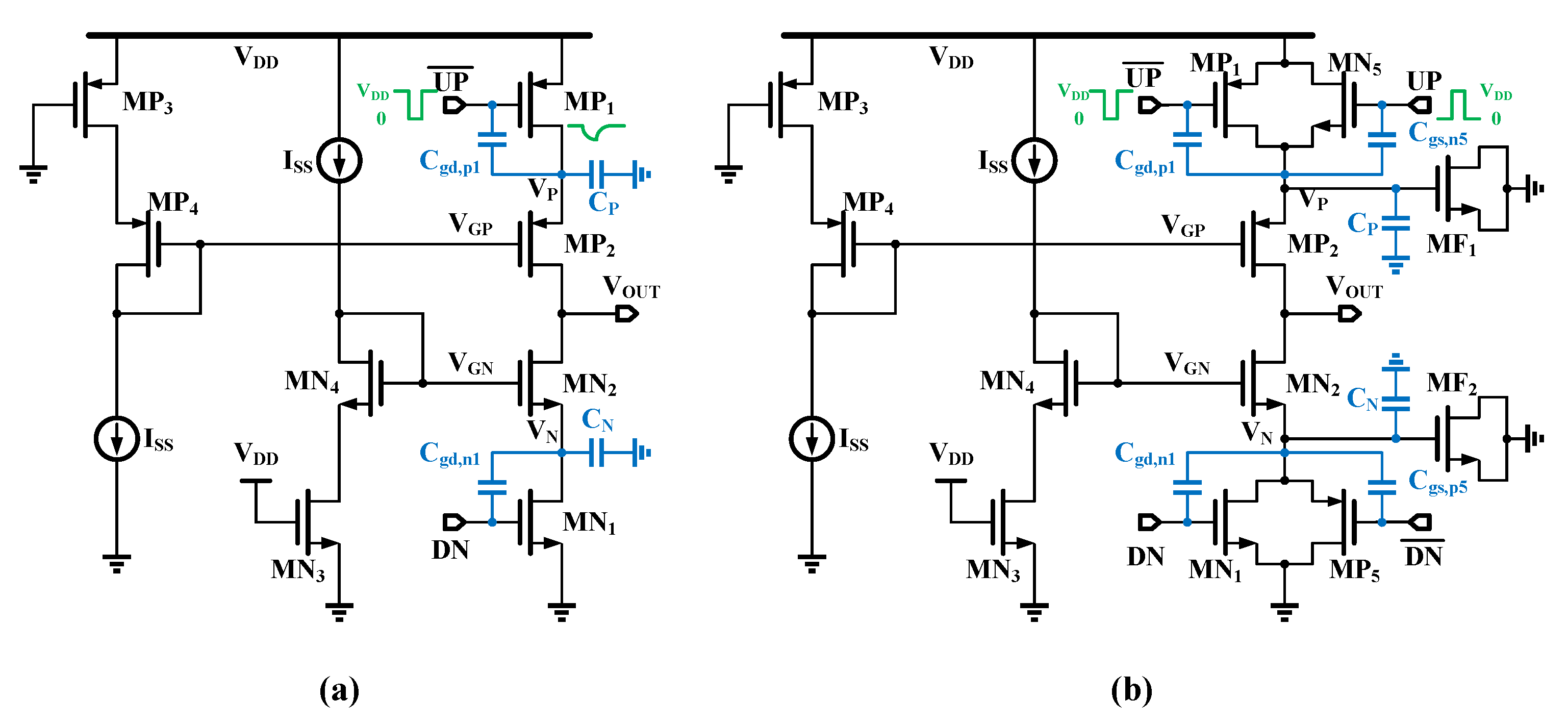
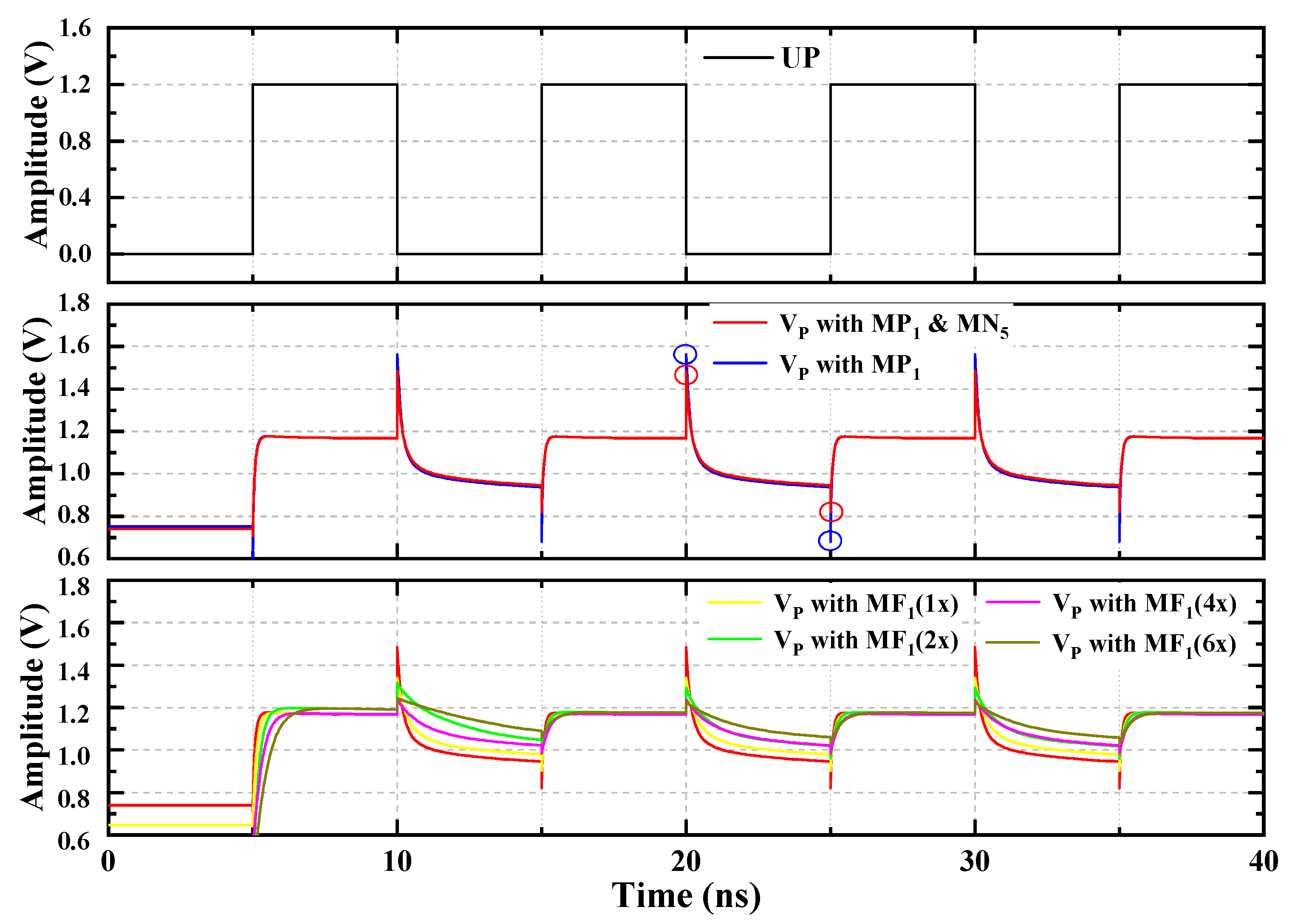
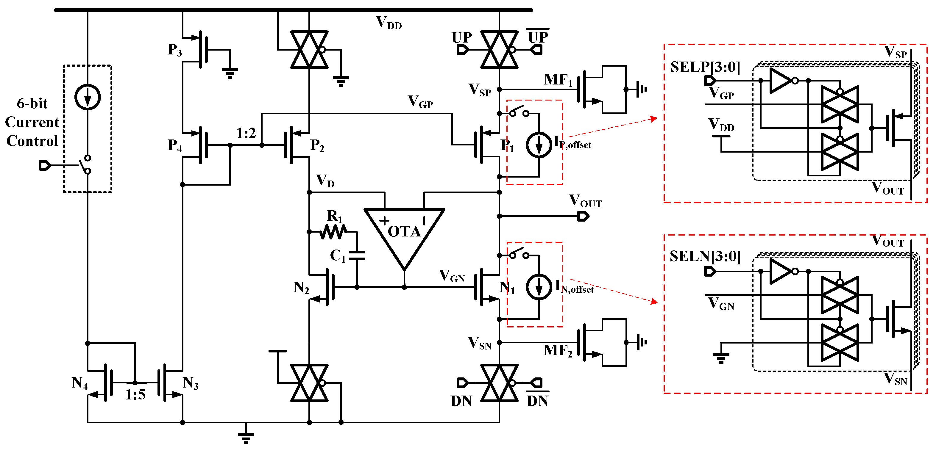
3.1. Clock Feedthrough Suppressed and Low Current Mismatch Charge Pump

The charge pump is a critical component in the proposed PLL design. It is responsible for generating the required voltage levels to control the loop dynamics. But in fact, there are many non-ideal factors in charge pumps, among which, current mismatch, clock feedthrough, charge sharing, and charge injection lead to non-idealities of the reference spur of PLL.
Among them, the clock feedthrough is caused by the gate–drain capacitor of the switched transistor, which leads to the high-frequency components being fed to the loop filter through this parasitic capacitor, thus leading to the deterioration of the PLL’s reference spurs. In order to reduce the influence of the clock feedthrough, it is a better choice to adopt the source-switched charge pump.
To mitigate the impact of the clock feedthrough, utilizing the conventional source-switched charge pump is proved to be a favorable option, as illustrated in Figure 2a. The source-switched charge pump can reduce the output voltage ripple compared to other charge pump architectures. By dynamically switching between current sources, it effectively mitigates the impact of switching transients and ripple noise. As a result, the output voltage exhibits improved smoothness and stability. In Figure 2a, MP 2 and MN 2 operate as current sources, and MP 1 and MN 1 operate as switches. Additionally, the switched transistors placed close to the power and ground improve the charging and discharging speed.
Indeed, along with its advantages, the source-switched structure also leads to negative effects resulting from the current mismatch. Their saturation currents in accordance with the channel length modulation effect can be expressed as
I U P = 1 2 μ p C o x ( W L ) P 2 ( V P V G P V t p ) 2 ( 1 + λ p | V O U T V P | )
I D N = 1 2 μ n C o x ( W L ) N 2 ( V G N V N V t n ) 2 ( 1 + λ n | V O U T V N | ) .
The clock signals are fed to the nodes V P and V N through C g d , p 1 and C g d , n 1 , which are the gate–drain capacitors of MP 1 and MN 1 , respectively, so that the node voltages of V P and V N change. When the voltages of nodes V P and V N change, I U P and I D N will change, which will lead to non-ideal factors. Assuming the equivalent capacitors of nodes V P and V N to the ground are represented as C P and C N , respectively, we note that the voltage variation at node V P due to clock feedthrough is given by V D D C g d , p 1 /( C g d , p 1 + C P ).
In order to reduce the influence of the clock feedthrough on nodes V P and V N , MP 1 and MN 1 are replaced by transmission gates, and MOS transistors with a filtering function are added at V P and V N to further reduce the influence of non-ideal factors, as shown in Figure 2b. The differential signals UP and U P ¯ , as well as DN and D N ¯ , undergo cancellation of the feedthrough signals upon passing through the transmission gates. Since C g d , p 1 and C g s , n 5 are generally not equal, a net amount of change appears at V P given by V D D ( C g d , p 1 C g s , n 5 )/( C g d , p 1 + C g s , n 5 + C P ). Moreover, due to the low-voltage operation of the charge pump, the transmission gate dimensions are increased to mitigate voltage drops. This enlargement of transmission gate dimensions, however, leads to larger parasitic capacitances within the transmission gates, facilitating favorable clock feedthrough conditions. Hence, it becomes imperative to further suppress the clock feedthrough at nodes V P and V N . To address this challenge while considering design simplification, we adopted the utilization of NMOS transistors, MF 1 and MF 2 , as a filtering mechanism. NMOS transistors were introduced at nodes V P and V N , as depicted in Figure 2b, exploiting their inherent parasitic capacitances ( C g s and C g d ) to facilitate the filtering process. It is noteworthy that the introduction of the filtering NMOS transistors is specific to the source-switched charge pump.
Figure 3 illustrates the impact of filtering NMOS transistors of different dimensions on the filtering effectiveness at the V P node. It is evident that, in the absence of filtering NMOS transistors, the voltage variation at node V P due to clock feedthrough with the transmission gate is less affected by clock feedthrough than without the transmission gate. Upon the integration of filtering NMOS transistors, an increase in the size of the filtering NMOS transistors MF 1 results in a more pronounced attenuation of feedthrough. However, with the increase in the capacitance of the filtering NMOS, the charging and discharging speeds of the current slows down, which leads to the unequal current copied by the current mirror and the current mismatch. Optimal results are achieved when the area of the filtering NMOS transistor is compromised with the filtering effect. Specifically, as can be seen from Figure 3, when the area of the filtering NMOS transistor is twice that of MP 1 , the trade-off between the charging and discharging speeds of the current and the filtering effect is good for achieving the desired feedthrough suppression. Another function of the filtering NMOS transistor is to reduce the voltage transients at the source terminal during feedthrough, as well as to mitigate the potential impact of signal coupling onto the gate terminal of the current mirror.
The current mismatch is one of the key factors contributing to the reference spur in the PLL. The amount of the reference spur is approximately calculated as [27]
P s p u r ( d B c ) = 20 l o g ( Δ ϕ 2 · N · B W f r e f ) 20 l o g ( f r e f f p )
where N is the frequency division ratio, BW is the PLL bandwidth, and f p is the frequency of the pole in the loop filter. Δ ϕ refers to the phase error. The major phase error contributors are the leakage currents, the current mismatch of the charge pump, and the switching time mismatch between the up and down current pulses. The analytic expression of the phase error is
Δ ϕ = Δ ϕ l e a k a g e + Δ ϕ c u r r e n t + Δ ϕ t i m e = 2 π · ( I l e a k a g e I C P + Δ I I C P · T s w i t c h T r e f + Δ T · T s w i t c h T r e f 2 )
where I l e a k a g e is the leakage current, I C P is the current of the charge pump, T s w i t c h is the frequency of reference clock, and Δ T, Δ I are the time and current mismatch, respectively.
Formulaes (8) and (9) show that the reference spur P s p u r is positively correlated with the current mismatch Δ I of the charge pump, which means that the reference spur can be scaled down by decreasing the current mismatch of the charge pump.
In order to effectively constrain the current mismatch within a limited range, additional bias current branches, namely I N , o f f s e t and I P , o f f s e t , introduced parallel to P 1 and N 1 in the charge pump to finely adjust the currents of both the pump-up and pump-down current mirrors. Figure 4 illustrates the proposed circuit configuration for the charge pump.
Due to the presence of the operational transconductance amplifier (OTA), the voltage at V O U T is equivalent to the voltage at V D . However, the existence of the transmission gates prevents the source voltages of P 1 /P 2 and N 1 /N 2 , which act as current mirrors, from being exactly equal. According to Formulae (6) and (7), a mismatch in currents occurs between the transistors P 1 and N 1 . Additionally, process deviations in MOS transistors contribute to pump-up and pump-down current mismatch.
To further mitigate the impact of the current mismatch-induced reference spur, the current compensation branches are introduced into the circuit, as depicted in Figure 4. When the switches are connected to the ground or the power supply, the compensation branches remain closed and do not participate in current compensation. However, when the switches are connected to the gate terminals of the parallel MOS transistors, the compensation branches become active, aiding in current compensation. Notably, the compensation branches’ minimum compensating current should not be excessively large, thus a minimum current of 2 µA is set with 4-bit compensation current branches.
Figure 5 illustrates the current mismatch effect under different process corners and temperatures. As observed from the graph, compensating through the bypass branch effectively limits the mismatch to below 0.1% across various process corners.
After designing the charge pump, it is necessary to conduct a linearity simulation for the cascade of the PFD and the charge pump. By changing the time error Δ T between the rising edge of the reference clock and the rising edge of the output of the loop feedback clock, the average output current of the charge pump can be viewed, as shown in Figure 6. As can be seen from the figure, when the time error Δ T is greater than zero, the average output current of the charge pump is positive, indicating that it is in a charging state at this time. When the time error Δ T is less than zero, the average output current of the charge pump is negative, indicating that it is in a discharging state at this time. However, with the increase of the time error Δ T, the average output current of the charge pump increases. When Δ T exceeds an integer multiple of the period of the reference clock, the average output current of the charge pump will change approximately periodically. When the rising edge of the reference clock coincides with the rising edge of the loop feedback clock, that is, Δ T is zero, the average output current of the charge pump is the mismatch current. After the charge pump is compensated, the average output current drops from 1.76 µA to 0.71 µA, which shows that the current mismatch between the charging current and the discharging current is 0.71 µA when the PLL is locked.

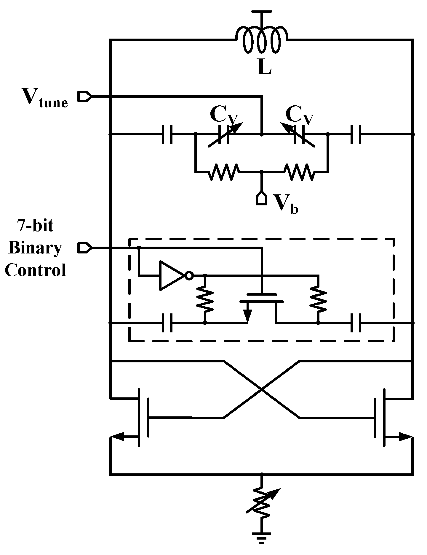
3.2. Wide-Tuning Range VCO

Figure 7 illustrates the schematic of a cross-coupled LC-VCO. The proposed VCO employs a differential topology consisting of NMOS transistors, which generate negative resistance to compensate for losses in the LC tank. To achieve current control, resistor-switched is utilized instead of a current mirror, as it contributes less flicker noise.
The current of the proposed VCO can be adjusted within a range of 0.5 mA to 15.5 mA, with a step size of 0.5 mA, utilizing a 6-bit resistor bank. For frequency tuning, the VCO incorporates a 7-bit binary-weighted metal–insulator–metal (MIM) capacitor bank for coarse tuning and varactors for fine-tuning. The designed VCO offers a tuning range from 1.9 GHz to 3.1 GHz. To characterize the VCO’s performance, an average gain (K V C O ) of 50 MHz/V is targeted, ensuring suitable frequency modulation capabilities.

3.3. Symmetrical CML Divider

CML dividers utilize differential voltage signaling, which offers several advantages. Firstly, differential signaling helps in rejecting noise, leading to improved signal integrity. Additionally, the differential nature of CML circuits enables seamless integration with other differential circuits present in the system, promoting compatibility and ease of design.
Moreover, CML dividers are capable of operating at high frequencies, making them suitable for applications that require the rapid division of clock signals or frequency synthesis. This attribute enhances their versatility and applicability in various systems.
The total frequency division ratio achieved by the cascade of multi-stage divide-by-2/3 circuits is calculated as 2 N to 2 N + 1 1 , where ’N’ represents the number of stages.
Figure 8 presents the block diagram of the proposed frequency divider utilized in this design. The frequency divider employs a four-stage cascade structure of divide-by-2/3 circuits, enabling a frequency division ratio ranging from 16 to 31. To further enhance the performance of the frequency divider, retiming technology is implemented.
The divide-by-2/3 circuit is depicted in Figure 9, and the circuit of the CML latch is depicted in Figure 10a. Due to the differential input and output nature of the CML divider, there exists a heightened requirement for circuit symmetry. In Figure 9, with the exception of the input terminals of AND2 and Latch2, which accommodate control signal B, the input terminals of the remaining AND gates and latches are driven by clock signals. In cases where input signals are not propelled by buffer elements, the conventional topology illustrated in Figure 10b may result in disparate differential input impedances within the AND gate. This incongruence in impedance is undesirable within a fully differential structure.
In response to this concern, an improved topology, as depicted in Figure 10c, has been devised. In this enhanced configuration, input signals A and B exhibit symmetric conditions, thus facilitating a more symmetrical design for the entire 2/3 divider. This symmetric arrangement is conducive to a more balanced design of the overall 2/3 divider, which is especially advantageous within the context of the CML divider’s imperative for heightened circuit symmetry.
CML circuits offer speed advantages due to two key properties. Firstly, they employ moderate voltage swings, which helps in achieving faster operation. Secondly, only NMOS devices are used in the data and clock paths, further enhancing the speed performance.
The output swing of the latch can be adjusted by varying the resistance value of R D , allowing for control of the static output bias voltage. This adjustment helps optimize the performance and characteristics of the CML latch circuit.
If the transistors switch completely, the single-ended output voltage swing of Output Q and Output Q ¯ can be expressed as
V p p = I S S R D
where V p p is the maximum single-ended output voltage swing of Output Q and Output Q ¯ . I S S is the average tail current and R D is the load resistance.
The output common mode (CM) level of Output Q and Output Q ¯ is given by:
V C M = V D D ( I S S R D ) / 2 .
To increase the maximum operating frequency of the divider, the current of the CML latch can be increased, but this may result in a reduction in the output swing and the driving ability of the latch becomes weak.

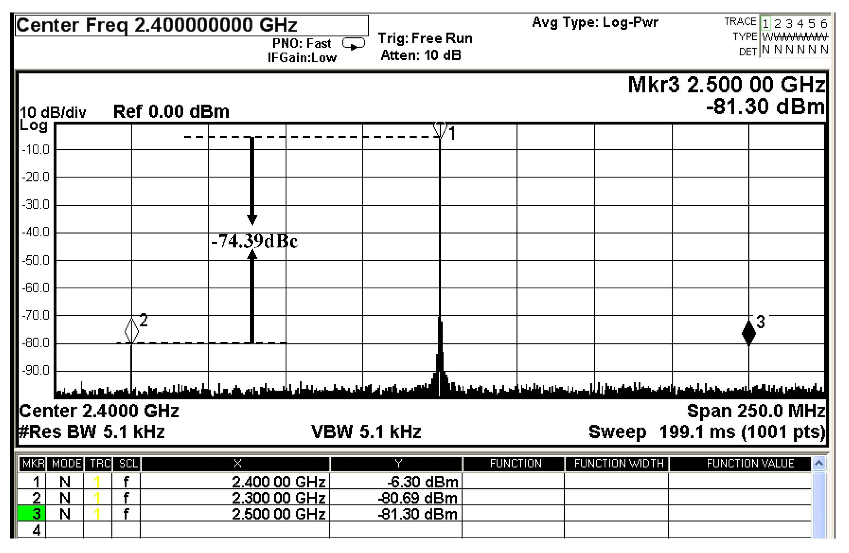
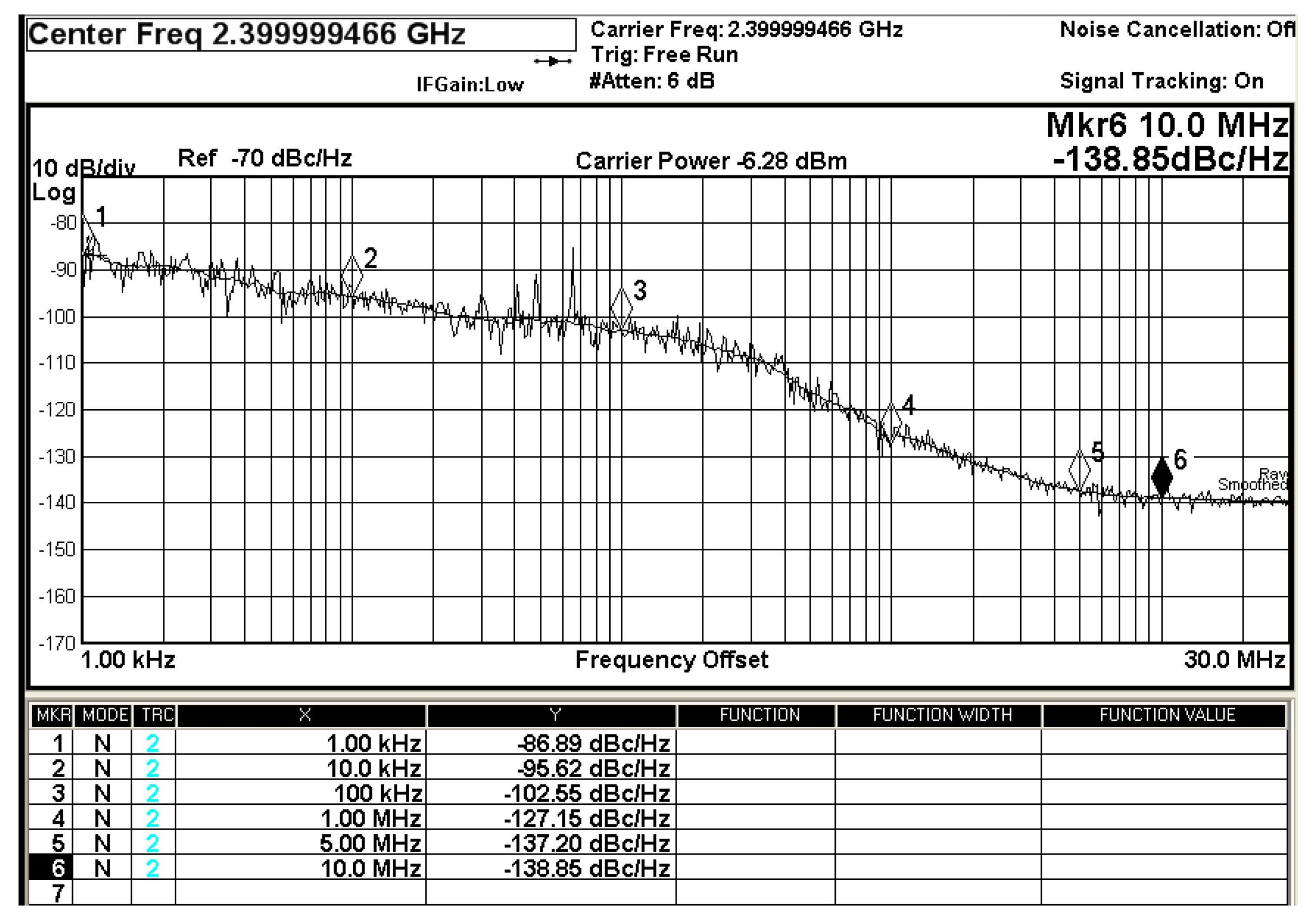
4. Measurement Results

The designed PLL is fabricated in a 130 nm CMOS technology process. The control code voltages, the frequency tuning voltage, and the DC supply are wire-bonded to a printed circuit board (PCB). The chip micrograph of the fabricated PLL is shown in Figure 11.
A PXA signal analyzer (Agilent N9030A, Agilent Technologies, Santa Clara, CA, USA) is used to measure the proposed PLL. During the test, the operating current of the VCO is set to 11.5 mA, and the branch current of the charge pump is set to 2 mA. At these settings, Figure 12 and Figure 13 show the output spectrum and the phase noise of the proposed PLL at a carrier frequency of 2.4 GHz, respectively. The reference spur of the PLL is −74.39 dBc below the carrier as shown in Figure 12. The measured phase noise of the PLL is −102.55 dBc/Hz@100kHz and −127.15 dBc/Hz@1MHz as displayed in Figure 13. The total power consumption of the proposed PLL is 33.6 mW from a 1.2 V supply. Among the components, the charge pump consumes 5.5 mA, the VCO core draws 11.4 mA from a 1.2 V supply voltage, and the divider dissipates 12.8 mA. In terms of jitter performance, the measured rms jitter integrated from 10 kHz to 10 MHz at a carrier frequency of 2.4 GHz is 340.99 fs. Additionally, the figure-of-merit (FoM) at the same carrier frequency is −234.08 dB.
Table 1 summarizes a comprehensive comparison of the performance between the proposed PLL and other PLLs reported in previous studies. The phase noise performance of the proposed PLL stands out significantly in comparison to the reported PLLs. In addition, the proposed wideband PLL achieves a tuning range of 40%, which is only narrower than that of [28]. The FoM of the proposed PLL is comparable to that of other works. However, it is worth noting that their reference spur is worse than the proposed PLL’s reference spur of −74.39 dBc.

5. Conclusions

We presented a comprehensive design of a wideband PLL with low reference spur and low phase noise. The charge pump employs a source-switched charge pump with additional bias current branches to minimize current mismatch, resulting in improved phase noise performance. The utilization of the 4-stage CML divide-by-2/3 circuit in the frequency divider enables high-speed frequency division without the limitations of narrowband resonator structures. The VCO design, incorporating a wide tuning range and adjustable tail resistor, optimizes the trade-off between phase noise and power consumption. The measured results demonstrate a frequency tuning range from 2.0 GHz to 3.0 GHz, with a remarkable tuning range of 40%. Notably, the PLL exhibits a reference spur of −74.39 dBc and a FoM of −234.08 dB at a carrier frequency of 2.4 GHz. The achieved performance levels and the significant advancements in phase noise and reference spur make the proposed wideband PLL a promising solution for high-speed wireless communication systems. The low phase noise and low reference spur characteristics enable stable and accurate frequency synthesis, contributing to improved data transmission and reception in future wireless communication applications.

Author Contributions

Conceptualization, Y.W.; data curation, Y.W., Y.L. and H.X.; validation, Y.W., Y.L. and H.X.; formal analysis, Y.W., Y.L. and H.X.; investigation, Z.L. (Zhongmao Li) and Z.L. (Zhiqiang Li); methodology, Y.W., Y.L. and H.X.; supervision, Y.W., Y.L. and H.X.; writing—original draft, Y.W.; writing—review and editing, Y.W., Y.L., H.X., Z.L. (Zhongmao Li) and Z.L. (Zhiqiang Li). All authors have read and agreed to the published version of the manuscript.

Funding

This research received no external funding.

Data Availability Statement

All the data are reported/cited in the paper.

Conflicts of Interest

The authors declare no conflict of interest.

References

  1. Debashis, M.; Bhattacharyya, T.K. 7.95 mW 2.4 GHz Fully-Integrated CMOS Integer N Frequency Synthesizer. In Proceedings of the 20th International Conference on VLSI Design Held Jointly with 6th International Conference on Embedded Systems (VLSID’07), Bangalore, India, 6–10 January 2007; pp. 156–164. [Google Scholar]
  2. Vamshi Krishna, M.; Xie, J.; Do, M.A.; Boon, C.C.; Yeo, K.S.; Do, A.V. A 1.8-V 3.6-mW 2.4-GHz fully integrated CMOS frequency synthesizer for IEEE 802.15.4. In Proceedings of the 2010 18th IEEE/IFIP International Conference on VLSI and System-on-Chip, Madrid, Spain, 27–29 September 2010; pp. 387–391. [Google Scholar]
  3. Wang, Z. An analysis of charge-pump phase-locked loops. IEEE Trans. Circuits Syst. I Regul. Pap. 2005, 52, 2128–2138. [Google Scholar] [CrossRef]
  4. Liao, T.-W.; Su, J.-R.; Hung, C.-C. Spur-Reduction Frequency Synthesizer Exploiting Randomly Selected PFD. IEEE Trans. Very Large Scale Integr. Syst. 2013, 21, 589–592. [Google Scholar] [CrossRef]
  5. Kong, L.; Razavi, B. A 2.4 GHz 4 mW Integer-N Inductorless RF Synthesizer. IEEE J. Solid-State Circuits 2016, 51, 626–635. [Google Scholar] [CrossRef]
  6. Zhang, X.; Liu, H.; Li, L. A low jitter phase-locked loop based on self-biased techniques. IEICE Electron. Express 2015, 12, 20150597. [Google Scholar]
  7. Mandal, D.; Mandal, P.; Bhattacharyya, T.K. Prediction of reference spur in frequency synthesisers. IET Circuits Devices Syst. 2015, 9, 131–139. [Google Scholar] [CrossRef]
  8. Kim, K.; Kim, K.; Yoo, C. A fREF/5 Bandwidth Type-II Charge-Pump Phase-Locked Loop with Dual-Edge Phase Comparison and Sampling Loop Filter. IEEE Microw. Wirel. Compon. Lett. 2018, 28, 825–827. [Google Scholar] [CrossRef]
  9. Mandal, D.; Mandal, P.; Bhattacharyya, T.K. Spur reducing architecture of frequency synthesiser using switched capacitors. IET Circuits Devices Syst. 2014, 8, 237–245. [Google Scholar] [CrossRef]
  10. Wang, H.Y.; Shou, G.L.; Wu, N.J. An adaptive frequency synthesizer architecture reducing reference sidebands. In Proceedings of the 2006 IEEE International Symposium on Circuits and Systems (ISCAS), Kos, Greece, 21–24 May 2006; p. 4. [Google Scholar]
  11. Li, A.; Chao, Y.; Chen, X.; Luong, H.C. A Spur-and-Phase-Noise-Filtering Technique for Inductor-Less Fractional-N Injection-Locked PLLs. IEEE J. Solid-State Circuits 2017, 52, 2128–2140. [Google Scholar] [CrossRef]
  12. Charles, C.T.; Allstot, D.J. A Calibrated Phase/Frequency Detector for Reference Spur Reduction in Charge-Pump PLLs. IEEE J. Solid-State Circuits 2006, 53, 822–826. [Google Scholar] [CrossRef]
  13. Hung, C.-M.; O, K.K. A fully integrated 1.5-V 5.5-GHz CMOS phase-locked loop. IEEE J. Solid-State Circuits 2002, 37, 521–525. [Google Scholar] [CrossRef]
  14. Gierkink, S.L.J. Low-Spur, Low-Phase-Noise Clock Multiplier Based on a Combination of PLL and Recirculating DLL with Dual-Pulse Ring Oscillator and Self-Correcting Charge Pump. IEEE J. Solid-State Circuits 2008, 43, 2967–2976. [Google Scholar] [CrossRef]
  15. Amer, A.G.; Ibrahim, S.A.; Ragai, H.F. A novel current steering charge pump with low current mismatch and variation. In Proceedings of the 2016 IEEE International Symposium on Circuits and Systems (ISCAS), Montreal, QC, Canada, 22–25 May 2016; pp. 1666–1669. [Google Scholar]
  16. Liang, C.-F.; Chen, S.-H.; Liu, S.-I. A Digital Calibration Technique for Charge Pumps in Phase-Locked Systems. IEEE J. Solid-State Circuits 2008, 43, 390–398. [Google Scholar] [CrossRef]
  17. Lin, W.-M.; Liu, S.-I.; Kuo, C.-H.; Li, C.-H.; Hsieh, Y.-J.; Liu, C.-T. A phase-locked loop with self-calibrated charge pumps in 3-µm LTPS-TFT technology. IEEE Trans. Circuits Syst. II Express Briefs 2009, 56, 142–146. [Google Scholar]
  18. Su, P.-E.; Pamarti, S. Mismatch shaping techniques to linearize charge pump errors in fractional-N PLLs. IEEE Trans. Circuits Syst. I Regul. Pap. 2010, 57, 1221–1230. [Google Scholar]
  19. Yang, P.; Guo, Y.; Jiang, H.; Wang, Z. A 360–456 MHz PLL frequency synthesizer with digitally controlled charge pump leakage calibration. In Proceedings of the 2019 IEEE Asian Solid-State Circuits Conference (A-SSCC), Macau, Macao, 4–6 November 2019; pp. 285–286. [Google Scholar]
  20. Luo, T.-N.; Chen, Y.-J.E. A 0.8-mW 55-GHz Dual-Injection-Locked CMOS Frequency Divider. IEEE Trans. Microw. Theory Tech. 2008, 56, 620–625. [Google Scholar]
  21. Tiebout, M. A CMOS direct injection-locked oscillator topology as high-frequency low-power frequency divider. IEEE J. Solid-State Circuits 2004, 39, 1170–1174. [Google Scholar] [CrossRef]
  22. Chen, Y.-T.; Li, M.-W.; Huang, T.-H.; Chuang, H.-R. A V-Band CMOS Direct Injection-Locked Frequency Divider Using Forward Body Bias Technology. IEEE Microw. Wirel. Compon. Lett. 2010, 20, 396–398. [Google Scholar] [CrossRef]
  23. Rong, S.; Ng, A.W.L.; Luong, H.C. 0.9 mW 7 GHz and 1.6 mW 60 GHz frequency dividers with locking-range enhancement in 0.13 µm CMOS. In Proceedings of the 2009 IEEE International Solid-State Circuits Conference—Digest of Technical Papers, San Francisco, CA, USA, 8–12 February 2009; pp. 96–97. [Google Scholar]
  24. Takatsu, K.; Tamura, H.; Yamamoto, T.; Doi, Y.; Kanda, K.; Shibasaki, T.; Kuroda, T. A 60-GHz 1.65 mW 25.9% locking range multi-order LC oscillator based injection locked frequency divider in 65 nm CMOS. In Proceedings of the IEEE Custom Integrated Circuits Conference 2010, San Jose, CA, USA, 19–22 September 2010; pp. 1–4. [Google Scholar]
  25. Wen, S.-H.; Huang, J.-W.; Wang, C.-S.; Wang, C.-K. A 60 GHz Wide Locking Range CMOS Frequency Divider using Power-Matching Technique. In Proceedings of the 2006 IEEE Asian Solid-State Circuits Conference, Hangzhou, China, 13–15 November 2006; pp. 187–190. [Google Scholar]
  26. Wang, H.; Hajimiri, A. A 19 GHz 0.5 mW 0.35 µm CMOS frequency divider with shunt-peaking locking-range enhancement. In Proceedings of the 2001 IEEE International Solid-State Circuits Conference, Digest of Technical Papers, ISSCC (Cat. No. 01CH37177), San Francisco, CA, USA, 5–7 February 2001; pp. 412–413. [Google Scholar]
  27. Maxim, A. Low-voltage CMOS charge-pump PLL architecture for low jitter operation. In Proceedings of the 28th European Solid-State Circuits Conference, Florence, Italy, 24–26 September 2002; pp. 423–426. [Google Scholar]
  28. Fan, Y.; Xiang, B.; Zhang, D.; Ayers, J.S.; Shen, K.-Y.J.; Mezhiba, A. 19.5 Digital Leakage Compensation for a Low-Power and Low-Jitter 0.5-to-5 GHz PLL in 10 nm FinFET CMOS Technology. In Proceedings of the 2019 IEEE International Solid-State Circuits Conference—(ISSCC), San Francisco, CA, USA, 17–21 February 2019; pp. 320–322. [Google Scholar]
  29. Kong, L.; Razavi, B. 25.7 A 2.4 GHz 4 mW inductorless RF synthesizer. In Proceedings of the 2015 IEEE International Solid-State Circuits Conference—(ISSCC), Digest of Technical Papers, San Francisco, CA, USA, 22–26 February 2015; pp. 1–3. [Google Scholar]
  30. Hsueh, Y.-L.; Cho, L.-C.; Shen, C.-H.; Tsai, Y.-C.; Chueh, T.-C.; Chang, T.-Y.; Hsu, J.-L.; Zhan, J.-H.C. 28.2 A 0.29 mm2 frequency synthesizer in 40 nm CMOS with 0.19 psrms jitter and <-100 dBc reference spur for 802.11 ac. In Proceedings of the 2014 IEEE International Solid-State Circuits Conference Digest of Technical Papers (ISSCC), San Francisco, CA, USA, 9–13 February 2014; pp. 472–473. [Google Scholar]
  31. Levantino, S.; Marzin, G.; Samori, C.; Lacaita, A.L. A Wideband Fractional-N PLL with Suppressed Charge-Pump Noise and Automatic Loop Filter Calibration. IEEE J. Solid-State Circuits 2013, 48, 2419–2429. [Google Scholar] [CrossRef]
  32. Park, P.; Park, D.; Cho, S. A 2.4 GHz Fractional-N Frequency Synthesizer with High-OSR ΔΣ Modulator and Nested PLL. IEEE J. Solid-State Circuits 2012, 47, 2433–2443. [Google Scholar] [CrossRef]
Figure 1. Block diagram of the proposed PLL.
Electronics 12 04164 g001
Figure 2. (a) Conventional source-switched charge pump. (b) Improved conventional source-switched charge pump.
Electronics 12 04164 g002
Figure 3. Simulation of the clock feedthrough effect.
Electronics 12 04164 g003
Figure 4. Schematic of the proposed source-switched charge pump.
Electronics 12 04164 g004
Figure 5. Simulated mismatch currents under different process corners and temperatures.
Electronics 12 04164 g005
Figure 6. Linearity simulation for the cascade of PFD and charge pump.
Electronics 12 04164 g006
Figure 7. Schematic of the proposed VCO.
Electronics 12 04164 g007
Figure 8. Block diagram of the proposed frequency divider.
Electronics 12 04164 g008
Figure 9. Block diagram of the divide-by-2/3 circuit.
Electronics 12 04164 g009
Figure 10. (a) Schematic of the CML latch. (b) Conventional topology of CML AND gate and latch. (c) Proposed topology of the CML symmetrical AND gate and latch.
Electronics 12 04164 g010
Figure 11. Chip micrograph of the proposed PLL.
Electronics 12 04164 g011
Figure 12. Output spectrum of the proposed PLL at a 2.4 GHz carrier frequency.
Electronics 12 04164 g012
Figure 13. Phase noise of the PLL at a 2.4 GHz carrier frequency.
Electronics 12 04164 g013
Table 1. Performance comparison with the state of the pulished PLLs.
ReferenceThis WorkISSCC’19 [28]ISSCC’15 [29]ISSCC’14 [30]JSSC’13 [31]JSSC’12 [32]
Technology (nm)13010454065130
Supply (V)1.20.91N/A1.2N/A
Oscillator TopologyLCRingRingLCLCLC
Reference freq. (MHz)10010022.6264060
Output freq. (GHz)2.43.22.43.8833.612.438
/freq. Range (GHz)/(2.0–3.0)/(0.5–5.0)/(2.0–3.0)/(3.276–3.883)/(3.0–4.0)/ N/A
Tuning Range (%)40164401728.6N/A
Phase Noise
(dBc/Hz)
@100 kHz−102.55N/A−109.18−105.49−103.62−102.27
@1 MHz−127.15N/A−113.78−123.06−103.79−99.63
RMS jitter (fs)340.991870970300972.91092.6
(10 k–10 M)(100 k–100 M)(1 k–200 M)(1 k–10 M)(3 k–30 M)(10 k–10 M)
FoM (dB) *−234.08−233−234.1−242−235.1−229.41
Reference Spur (dBc)−74.39−57−65N/A−71−54.7
*: FoM = 20log(J r m s /1 s) + 10log(P D C /1 mW).
Disclaimer/Publisher’s Note: The statements, opinions and data contained in all publications are solely those of the individual author(s) and contributor(s) and not of MDPI and/or the editor(s). MDPI and/or the editor(s) disclaim responsibility for any injury to people or property resulting from any ideas, methods, instructions or products referred to in the content.

