
A New Unit-Cell Design for a 2-Bit Reflective Metasurface for RIS Applications


1
Smart Natural Space Research Center, Kongju National University, Cheonan 31080, Republic of Korea
2
Department of Smart Information and Technology Engineering, Kongju National University, Cheonan 31080, Republic of Korea
*
Author to whom correspondence should be addressed.
Electronics 2023, 12(20), 4220; https://doi.org/10.3390/electronics12204220
Submission received: 19 September 2023
/
Revised: 6 October 2023
/
Accepted: 10 October 2023
/
Published: 12 October 2023
(This article belongs to the Section Microwave and Wireless Communications)
Abstract
:In this research, a novel unit-cell design for a 2-bit reflective metasurface using the theory of characteristic modes is presented. The initial unit-cell consists of three sub-patches with 2-PIN diodes integrated within the gaps between sub-patches. The initial structure provides limited tuning of the phase curves with the change in switching states of PIN diodes. To provide the phase deviation required for the 2-bit operation, the symmetry of the modal currents is used to propose multiple slots in the sub-patches. Slots are introduced to lower the resonant frequencies, as well as provide tuning of the resonance of modes and consequently phase change between different switching states. For further resonance tuning and phase optimization, two vias are loaded in the middle patch to provide a 90° phase difference between each switching state. Simulated results show that the proposed unit-cell design with the aid of characteristic modes has a smaller size and provides 2-bit operation in the frequency range of 3.9–4.04 GHz.
1. Introduction
The 5G and 6G environments suffer from severe path losses, blind spots, and limited coverage [1]. Due to the uncontrolled nature of the wireless environment, a lot of efforts have been made to reduce these losses, and multiple solutions have been reported in the literature. Nevertheless, there are certain limitations associated with these solutions, such as the multiple input multiple output (MIMO) system, which mitigates the path losses by using high gain arrays; however, it does not address the signal blockage problem. The problem of blind spots can reportedly be reduced by increasing the density of base stations, but this demands large infrastructure, hence making it expensive and tending to consume more power. Reconfigurable intelligent surface (RIS), on the other hand, provides a cost- as well as power-efficient alternative to resolve these issues [2,3,4,5]. RIS improves the coverage and quality of signal by intelligently controlling the propagation environment. RIS uses low-cost reflecting metasurface (MTS) integrated with switching components like PIN diodes [6,7,8,9,10,11,12,13,14,15,16,17], varactor diodes [18,19], and a smart controllers. MTS exhibits special properties due to its ability to modify the incident electromagnetic (EM) waves on its surface. MTS modifies the EM waves on a sub-atomic level, thereby the response of the reflecting wave from the surface depends on the shape, size, and periodic arrangement of unit-cells. For the same aperture size, more unit cells with a smaller size relative to wavelength can be accommodated as compared to the large unit-cell. Using smaller unit-cells improves the directivity of a 1- and 2-bit programmable reflective MTS [20], an acceptable precision level of steering, and improved sidelobe levels are achieved even with the small-sized MTS.
A PIN diode integrated with MTS dynamically controls the amplitude and phase of the reflected wave; the phase response is controlled in a programmable manner and is mapped as n-bits based on the deviation between the phase of adjacent states. The number of diodes in the structure is determined by the number of bits and, usually, one PIN diode is required for 1-bit operation and two PIN diodes provide 2-bit operation. Currently, plenty of research is going on to design new unit cells, a 1-bit digital metasurface unit-cell is designed by connecting a PIN diode between two similarly slotted rectangular sub-patches [6], and a microstrip patch also works as a tunable resonator and provides 1-bit operation using the phase delay lines integrated with a pin diode [8]. The higher number of bits requires more PIN diodes, which increases the design complexity. Nevertheless, the number of bits is an important factor in RIS operations, and when the size of RIS is not infinite, for a better data, rate the number of bits should be higher than one [21]. Moreover, high-phase quantization provides better performance in terms of high directivity and low sidelobe levels [22,23]. The 2-pin diodes integrated with MTS unit-cells usually provide 2-bit phase quantization by providing four states with a phase difference of 90° between two states [9]. In [11], a single-layer unit-cell is realized by using folded ground, 2-PIN diodes, and wall of vias. A U-shaped dipole integrated with PIN diodes is designed for wireless power applications [12]. In [17], a fully functional unit-cell of RIS is presented; however, the structure is complex, large in size and thickness, and a higher number of pin diodes are used for the 2-bit operation.
The theory of characteristic modes (TCM) [24,25,26] provides deep physical insight into the radiating mechanism of arbitrarily shaped structures and is widely being employed to resolve complex antenna design problems. Insight is provided in terms of the currents, fields, modal significance MS, and characteristic angle values. MS is provided in Equation (1)
where are eigenvalues, these values represent the ratio of stored energy and radiated energy. Eigenvalues identify the radiating properties of modes using an infinite range of values. MS, on the other hand, states the radiating capability of a mode using the values in a limited range from [0, 1]. Modes with provide better radiations.
The characteristic angle is provided by Equation (2)
The resonant frequency of a mode is determined from the MS peak, i.e., when MS = 1 and the characteristic angle value correspondingly is .
TCM is being widely used to design high-performance metasurfaces for multiple applications which include but are not limited to circular polarization, wide bandwidth, and polarization conversion [27,28,29,30,31,32,33]. Circular polarization is achieved by exciting orthogonal modes and mode suppression is utilized for the high performance [27]. The high gain antenna is designed by exciting fundamental mode and suppressing irrelevant modes in the structure [28]. The wideband metasurface is designed by using multilayer array [29], and multimode resonances are also introduced in metasurfaces for wideband applications [30]. A study of the amplitude of reflection coefficients of the structure with the PIN diodes is performed to aid in the design of dual-polarized resorber in [31]. An active frequency selective surface is designed using the fundamental mode of the structure; the design involves the improvement of isolation between the two states transparent/reflective using CMA [32]; however, the technique only involves the study of the amplitude of s-parameters. The deviation between the characteristic angle values has also been studied to achieve polarization conversion in metasurfaces [33]. Most of the reported designs provide insight into the working mechanisms of structures using the amplitude of the s-parameters. The effect of the lumped resistors on the resonant properties is also studied in [34,35]. A frequency selective surface with resistive loading has also been studied using the modes. In [34], phase curves, as well as the amplitude of the reflection coefficients, are studied, and it is found that with the increase in resistance value, modal curves move to higher resonance. An absorber with polarization insensitivity and wider bandwidth is designed in [35], and the position of the lumped resistors is determined using the modal currents and fields. Absorption bandwidth is increased by properly locating the loading of the lumped resistors. Nevertheless, the phase properties of the modes are studied without consideration of the effect of switching elements.
In this research, a new unit-cell design is proposed for a 2-bit reflective metasurface using the theory of characteristic modes. Using the insight provided by the theory of characteristic modes and size miniaturization, an approach to tune phase curves for the 2-bit operation is provided. The paper is organized as it follows: in Section 2.1, initial unit-cell is studied using the theory of characteristic modes, and in Section 2.2, miniaturization is achieved. Further modal tuning for the 2-bit operation and structure optimization is provided in Section 2.3. The design is verified by using Floquet port boundary conditions in Section 3.
2. Analysis, Modeling, and Design of Unit-Cell Using Theory of Characteristic Modes
In this section, analysis of modes with the change in switching states of PIN diodes, the operating principle of multibit meta-cell using characteristic modes, and the evolution of the new unit-cell for 2-bit reflective metasurface is presented. The design evolution of the proposed unit-cell (MTS-III) is depicted in Figure 1. An MTS unit-cell has three sub-patches, a substrate layer of RT/Duriod 5880 with a thickness of 1.57 mm, and a ground is placed underneath the substrate layer. The size of the gap between sub-patches is equal to the size of the PIN diode, and to introduce 2-bit operation, two pin diodes are incorporated in the gap between sub-patches. Dimensions of the proposed geometry are provided in Table 1. Based on the switching operation of D1–D2 switching states OFF–OFF, ON–OFF, OFF–ON, and ON–ON correspond to State 00, State 10, State 01, and State 11, respectively.
2.1. Initial Unit-Cell (MTS-I) Design and Analysis
Characteristic mode analysis (CMA) of MTS-I with the open gaps between sub-patches shown in Figure 2 is performed using CST in the frequency range of 5–7.5 GHz, MS and characteristic angle values of the structure are plotted in Figure 3. For brevity, only the modes with the horizontal current symmetries are provided. Two radiating modes are identified within the band as depicted by the solid curves in Figure 3; Mode 1 is resonant at 5.65 GHz, while Mode 2 is resonant at 6.35 GHz. Corresponding to the resonance of both modes, the width of PL and PR is about the size of . The smaller width of PM (compared to PL and PR) is chosen to retain miniaturization, since its size is irrelevant to the resonant frequencies of both modes. Currents of both modes are plotted at their resonant frequencies in Figure 4; it can be seen that modes have horizontal current symmetries. To provide tuning of resonance of both modes, two diodes are incorporated within the gaps between sub-patches, and CMA of MTS-I with different switching states is performed. An illustration of the PIN diode (D1 and D2) integration in the gaps for the alternate ON and OFF switching states is provided in Figure 2. For CMA simulations of unit-cell with different combinations of the switching states, diodes are modeled using the conditions as provided in Table 2. In CMA, the PIN diode in the OFF state is modeled by the gap, while for the ON state, a stub is connected between sub-patches. Using the conditions stated in Table 2, an illustration of the model of PIN diodes in the ON state D1–D2 (ON–ON “State 11”) is depicted in Figure 2.
From the MS graph in Figure 3, we can see that the MS curve of Mode 1 in State 00 overlaps State 10, and State 01 overlaps State 11, depicting 0° phase change when switching takes place between these states. Characteristic angle curves corresponding to the MS values for State 00 and State 10, and State 01 and State 11, validate no phase changes when the switching operation takes place between the mentioned states. Nevertheless, for Mode 1, switching states from State 00 to State 11 or State 01 provide phase changes. The same is the case for State 10. A similar trajectory is followed by Mode 2, as the curves of Mode 2 for State 00 and State 01, and State 11 and 10, overlap. Since no states are providing phase changes, MTS-I does not provide 2-bit operation; therefore, modifications in the geometry are proposed in Section 2.2.
2.2. Proposed Slots for Tuning of Modes and Size Miniaturization Using CMA (MTS-II)
In this section, modifications in the MTS-I are proposed to provide 2-bit operation. Slots are loaded in the MTS-I using the modal currents in Figure 4. Slots are loaded to provide:
- 1.
- The tuning of the modes to achieve 2-bit operation;
- 2.
- The size miniaturization by moving modes to lower resonance.
In Section 2.1, it is found that MTS-I does not provide a change in the phase curve for Mode 1 and Mode 2 when D1 and D2 is turned ON, respectively. Therefore, slots are proposed in sub-patches of MTS-I to modify the structure and provide the deviation in the phase curves for both modes in each switching state. Rectangular slots are loaded to reduce the resonant frequencies of both modes. Different sets of slots are loaded in individual sub-patches to reduce the resonant frequencies, tuning the resonance frequencies of modes, and phase deviation between alternate switching states of each mode. To provide insight into the design evolution from MTS-I to MTS-II, slot loading in the individual sub-patches is presented in this section. It is worth mentioning that slots in each sub-patch provide tuning for one of the modes within the band. Currents of mode 2 have high density in PR, therefore slots are loaded in PR (Figure 4) to perturb Mode 2. Modification along the top and bottom edges of PR perturbed the resonant frequency of Mode 2. Slots provide the elongated path to the horizontal currents, consequently changing the resonant frequency from 6.35 GHz to 4.634 GHz. Two rectangular slots are loaded along the top and bottom edges of the right sub-patch (PR). Nevertheless, Mode 1 has low current density in PR; as a result, its resonance is unaffected and is still resonant at 5.67 GHz. Now referring to the slots in PL, since Mode 1 has high current density in PL (Figure 4), modifications along the horizontal currents in PL perturbed the resonance of Mode 1. Slots elongated the current paths and lowered the resonance of Mode 1 from 5.65 GHz to 4.53 GHz. Three rectangular slots are horizontally loaded in the left sub-patch (PL) to elongate the current paths for Mode 1 and move it to lower resonance. Nevertheless, modification has the least impact over the resonance of Mode 2 due to lower current density and is resonant at 6.37 GHz. The geometry of the modified unit-cell (MTS-II) is provided in Figure 1. After studying slots individually in PL and PR, further tuning for the 2-bit operation is performed by incorporating slots in PM. Rectangular slots incorporated along the top and bottom edges of PM further elongate the current paths for Mode 2. To further adjust the phase, a rectangular slot is loaded in sub-patch PM, location of the slot is chosen to be slightly offset from the center and closer to the edge near PL. This slot provides further tuning for the alternate switching between State 10 and State 01.
After incorporating slots in PM, CMA of MTS-II is carried out in the frequency range of 4–5.5 GHz. MS and characteristic angles of MTS-II are plotted in Figure 5. Solid curves (State 00) in Figure 5 indicate that Mode 1 is resonant at 4.49 GHz, while Mode 2 is resonant at 4.625 GHz. From the modal currents in Figure 6, we can see that slots significantly reduced the frequencies of resonant modes of MTS-I. From the MS and characteristic angles, we can see that both modes are providing tuning of resonance with the subsequent change in the switching states. A comparison of Figure 3 and Figure 5 depicts slight variation in the resonance, consequently inconsiderable phase deviation of Mode 1 due to the change between State 00 and State 10 is achieved. MS and characteristic angle curves for Mode 2 in State 00 and State 01 are still overlapping, indicating no phase change. Nevertheless, the phase difference required for the 2-bit operation around 4.5 GHz is not provided by the modes in the stated switching states. The rest of the switching states for both modes are grouped together around 5 GHz, with a very small phase deviation between each of the states in Figure 5, which does not fulfill the requirements for the 2-bit operation. Therefore, the structure needs further optimization, and the proposed modification for further tuning is provided in the next section.
2.3. Optimization of Proposed Design (MTS-III) for 2-Bit Operation
Further tuning of the modes desired for the 2-bit operation is performed in this section. Two vias are loaded in sub-patch PM. Vias are connecting PM to the ground and are loaded in the vicinity of the low current density region of Mode 2 shown in Figure 6. The optimized location and separation between vias is depicted in Figure 1. CMA of MTS-III in Figure 7 reveals that Mode 1 is resonant at 4.09 GHz, while Mode 2 is resonant at 4.518 GHz. Comparing currents of Mode 1 State 00 at 4.09 GHz in Figure 8 with Mode 2 in Figure 6, it is found that, due to vias, the frequency of this mode is significantly reduced, while a slight reduction in the frequency of mode 2 State 00 in Figure 8 is observed. MS and characteristic angle values plotted in Figure 7 for Mode 1 and Mode 2 at all switching states depict the changes in the resonant frequency of each mode with the change in every switching state. It can be seen that tuning performance is depicted in two regions of the curves, highlighted by the orange and blue rectangles, which indicates that the frequency of the tuning operation is defined by the fundamental modes of the unit-cell. To consider phase for all four states, it is seen that around 4.09 GHz, the nearest modes in other switching states to Mode 1 State 00 are: Mode 1, State 01; Mode 2, State 10; and Mode 2, State 11. Referring to the characteristic angle curves around 4.13 GHz, following the stated order of modes, the orange label from Equations (1)–(3) depicts the phase differences between Mode 1, State 00 and Mode 1, State 01; Mode 1, State 01 and Mode 2, State 10; and Mode 2, State 10 and Mode 2, State 11. Hence, there are two modes with different switching states. Modes in different switching states lying nearest to Mode 2 State 00 are: Mode 1, State 01; Mode 2, State 10; and Mode 2, State 11; highlighted by the blue rectangle. Hence, characteristic angle values around 4.3 GHz indicate phase difference between the mentioned states as indicated by the blue labels from Equations (4)–(6). Therefore, it is concluded that the nearest state irrespective of the mode index provides the phase deviation required for the 2-bit operation.
Currents of the modes providing 2-bit performance in the highlighted regions are shown in Figure 8. It is observed that, for Mode 1 in States 00 and 01, currents have high density in the sub-patches PM and PR, while the current density of Mode 2 is higher in the sub-patch PL in States 00 and 10. Currents of both modes in State 11 have high density in PL and PR.
A size comparison of MTS-I, MTS-II, and MTS-III in terms of the wavelength is provided in Table 3. The total length, width, and thickness of unit cells are calculated using the dimensions provided in Table 1. Size in terms of the wavelength is calculated using the frequencies of both modes. It is observed that slots provide the size reduction of 20.6% and 27.2% from MTS-I to MTS-II in the first and second bands, respectively. After incorporating vias, a further size reduction of about 8.86%, and 2.5% from MTS-II to MTS-III in the first and second bands, respectively, is achieved. Therefore, due to the proposed slotting and vias loading, an overall size reduction of almost 29.46% and 29.7% is achieved in the first and second band of the proposed geometry.
3. MTS-III Floquet Port Simulations
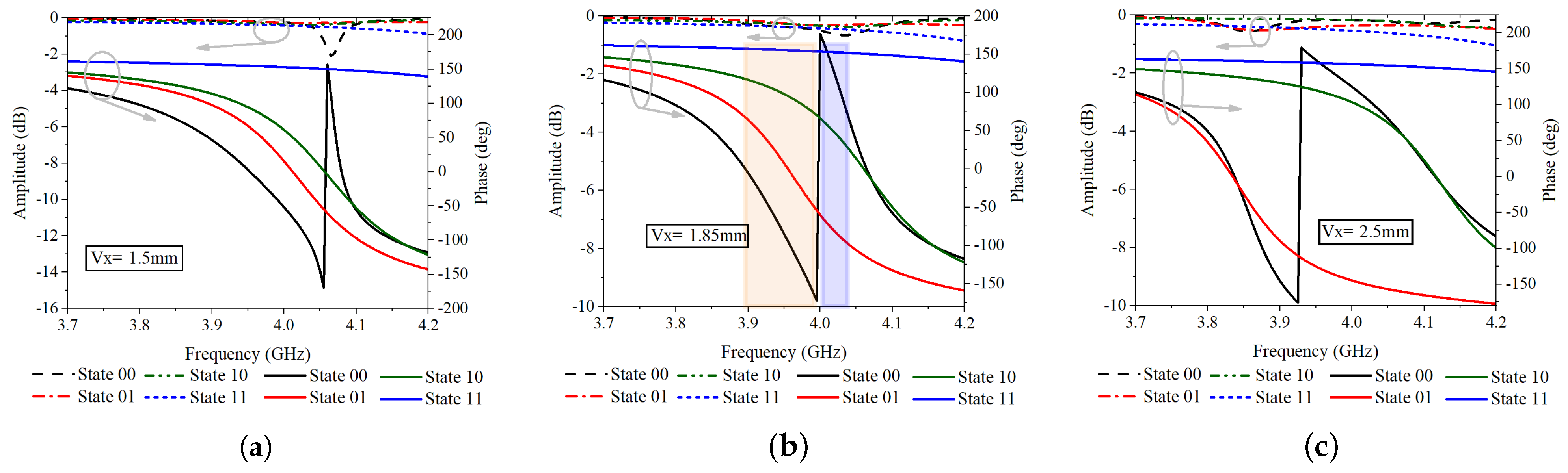
The MTS-III unit-cell is simulated in HFSS using periodic boundary conditions and Floquet port. PIN diode MADP-000907-14020 is modeled by a series LR circuit in the ON state, and a series LC circuit in the OFF state as provided in Figure 9. In order to tune the phase response for the 2-bit operation, a parametric analysis with the change in location of the vias by moving away from the center of sub-patch PM is performed as shown in Figure 10. The reflection response of the optimum MTS-III shows the magnitude response around −0.8 dB, while the phase difference between the adjacent states is 90° around 3.915 GHz. The shaded yellow and blue area under the curve highlights the region where MTS-III is providing 2-bit operation in Figure 10. Shaded areas correspond to the highlighted modes and resonances in Figure 7. Comparing both figures, we can see that in the orange shaded area of Figure 10 around the 3.915 GHz 90° phase difference is obtained between State 00 and State 01, State 01 and State 10, and State 10 and State 11. This is the same order as observed by the characteristic modes, therefore results corroborate the highlighted Equations (1)–(3) in Figure 7. Similarly, in the blue-shaded region in Figure 10, around 4.025 GHz is achieved between State 01 and State 10, State 10 and State 00, and State 00 and State 11. The same order is achieved by the CMA in Equations (4)–(6) in Figure 7. After comparing frequencies of 2-bit operation in the shaded region of Figure 10 with Figure 7, slight variations between the frequencies of CMA and Floquet port-based simulations are observed. The difference between frequencies is due to the use of lossless substrate in CMA, and the change in the location of vias for the optimization of design in the Floquet port simulations.
4. Comparison Table
A comparison of the proposed design with the reported work is provided in Table 4. From the comparison, we can see that the proposed structure provides 2-bit operation with a less complex structure and smaller size.
5. Conclusions
In this research, a small unit-cell design for the 2-bit reflective metasurface is proposed using the theory of characteristic modes. Using the modal currents, slots are proposed in the structure to tune the resonant frequencies of the modes. Tuning of the resonance is used to change the characteristic angles of two modes of an underlying structure. Multiple slots incorporated in the sub-patches reduced the frequency ratio between the two modes and also provided tuning of the phase deviation between different switching states of the PIN diodes. For further optimization of the 2-bit operation of the unit cell, two vias are also incorporated in the design. The proposed characteristic modes based design is also validated using the Floquet port boundary conditions. The proposed design provides a 2-bit performance with the band from 3.9 to 4.04 GHz. The structure provides amplitude response of −0.8 dB in the entire band. In comparison to the unit cell with rectangular sub-patches, the proposed structure provides the size miniaturization of about 29.46% and 29.7% in the first and second band, respectively.
Author Contributions
Conceptualization, I.-P.H.; Methodology, D.F.; Software, D.F.; Writing—original draft, D.F.; Writing—review & editing, I.-P.H.; Supervision, I.-P.H.; Project administration, I.-P.H.; Funding acquisition, I.-P.H. All authors have read and agreed to the published version of the manuscript.
Funding
This research was supported in part by Korea Basic Science Institute (National Research Facilities and Equipment Center) Grant 2022R1A6C101A741 funded by the Ministry of Education, in part by the Basic Science Research Program under Grant 2020R1I1A3057142, and in part by the Priority Research Center Program through the National Research Foundation under Grant 2019R1A6A1A03032988.
Conflicts of Interest
The authors declare no conflict of interest.
References
- Pan, C.; Ren, H.; Wang, K.; Kolb, J.F.; Elkashlan, M.; Chen, M.; Di Renzo, M.; Hao, Y.; Wang, J.; Swindlehurst, A.L.; et al. Reconfigurable Intelligent Surfaces for 6G Systems: Principles, Applications, and Research Directions. IEEE Commun. Mag. 2021, 59, 14–20. [Google Scholar] [CrossRef]
- Yildirim, I.; Uyrus, A.; Basar, E. Modeling and Analysis of Reconfigurable Intelligent Surfaces for Indoor and Outdoor Applications in Future Wireless Systems. IEEE Trans. Commun. 2021, 69, 1290–1301. [Google Scholar] [CrossRef]
- Wu, Q.; Zhang, R. Towards Smart and Reconfigurable Environment: Intelligent Reflecting Surface Aided Wireless Network. IEEE Commun. Mag. 2020, 58, 106–112. [Google Scholar] [CrossRef]
- Hu, J.; Zhang, H.; Di, B.; Li, L.; Bian, K.; Song, L.; Li, Y.; Han, Z.; Poor, H.V. Reconfigurable Intelligent Surface Based RF Sensing: Design, Optimization, and Implementation. IEEE J. Sel. Areas Commun. 2020, 38, 2700–2716. [Google Scholar] [CrossRef]
- Rana, B.; Cho, S.S.; Hong, I.P. Review Paper on Hardware of Reconfigurable Intelligent Surfaces. IEEE Access 2023, 11, 29614–29634. [Google Scholar] [CrossRef]
- Cui, T.J.; Qi, M.Q.; Wan, X.; Zhao, J.; Cheng, Q. Coding metamaterials, digital metamaterials and programmable metamaterials. Light. Sci. Appl. 2014, 3, e218. [Google Scholar] [CrossRef]
- Zhou, Y.; Chen, L.; Zhang, Q.; Wang, H.; Guo, L. A 1-bit reconfigurable intelligent metasurface-based antenna design for 5G application. Int. J. Microw. Wirel. Technol. 2023, 1–10. [Google Scholar] [CrossRef]
- Cao, X.; Chen, Q.; Tanaka, T.; Kozai, M.; Minami, H. A 1-bit Time-Modulated Reflectarray for Reconfigurable-Intelligent-Surface Applications. IEEE Trans. Antennas Propag. 2023, 71, 2396–2408. [Google Scholar] [CrossRef]
- Saifullah, Y.; Chen, Q.; Yang, G.; Waqas, A.; Xu, F. Dual-band multi-bit programmable reflective metasurface unit cell: Design and experiment. Opt. Express 2021, 29, 2658–2668. [Google Scholar] [CrossRef] [PubMed]
- Hodge, J.A.; Spence, T.G.; Zaghloul, A.I. A Reconfigurable Intelligent Surface Using a 2-Bit Programmable Metasurface for Communications. In Proceedings of the 2021 IEEE International Symposium on Antennas and Propagation and USNC-URSI Radio Science Meeting (APS/URSI), Singapore, 4–10 December 2021; pp. 97–98. [Google Scholar]
- Li, P.; Ren, J.; Chen, Y.; Ren, X.; Xu, K.D.; Yin, Y.Z.; Shen, M. Design of Low-Cost Single-Layer 2-Bit Reflective Programmable Metasurface Based on Folded Ground. IEEE Trans. Microw. Theory Technol. 2023, 71, 3455–3465. [Google Scholar] [CrossRef]
- Han, J.; Li, L.; Ma, X.; Gao, X.; Mu, Y.; Liao, G.; Luo, Z.J.; Cui, T.J. Adaptively smart wireless power transfer using 2-bit programmable metasurface. IEEE Trans. Ind. Electron. 2021, 69, 8524–8534. [Google Scholar] [CrossRef]
- Zhang, L.; Chen, X.Q.; Shao, R.W.; Dai, J.Y.; Cheng, Q.; Castaldi, G.; Galdi, V.; Cui, T.J. Breaking Reciprocity with Space-Time-Coding Digital Metasurfaces. Adv. Mater. 2019, 31, 1904069. [Google Scholar] [CrossRef]
- Zhang, L.; Wang, Z.X.; Shao, R.W.; Shen, J.L.; Chen, X.Q.; Wan, X.; Cheng, Q.; Cui, T.J. Dynamically Realizing Arbitrary Multi-Bit Programmable Phases Using a 2-Bit Time-Domain Coding Metasurface. IEEE Trans. Antennas Propag. 2019, 68, 2984–2992. [Google Scholar] [CrossRef]
- Ma, Q.; Bai, G.D.; Jing, H.B.; Yang, C.; Li, L.; Cui, T.J. Smart metasurface with self-adaptively reprogrammable functions. Light. Sci. Appl. 2019, 8, 98. [Google Scholar] [CrossRef]
- Huang, C.; Sun, B.; Pan, W.; Cui, J.; Wu, X.; Luo, X. Dynamical beam manipulation based on 2-bit digitally-controlled coding metasurface. Sci. Rep. 2017, 7, 42302. [Google Scholar] [CrossRef]
- Dai, L.; Wang, B.; Wang, M.; Yang, X.; Tan, J.; Bi, S.; Xu, S.; Yang, F.; Chen, Z.; Di Renzo, M.; et al. Reconfigurable Intelligent Surface-Based Wireless Communications: Antenna Design, Prototyping, and Experimental Results. IEEE Access 2020, 8, 45913–45923. [Google Scholar] [CrossRef]
- Sayanskiy, A.; Belov, A.; Yafasov, R.; Lyulyakin, A.; Sherstobitov, A.; Glybovski, S.; Lyashev, V. A 2D-Programmable and Scalable Reconfigurable Intelligent Surface Remotely Controlled via Digital Infrared Code. IEEE Trans. Antennas Propag. 2023, 71, 570–580. [Google Scholar] [CrossRef]
- Liang, J.C.; Cheng, Q.; Gao, Y.; Xiao, C.; Gao, S.; Zhang, L.; Jin, S.; Cui, T.J. An Angle-Insensitive 3-Bit Reconfigurable Intelligent Surface. IEEE Trans. Antennas Propag. 2022, 70, 8798–8808. [Google Scholar] [CrossRef]
- Taghvaee, H.; Abadal, S.; Pitilakis, A.; Tsilipakos, O.; Tasolamprou, A.C.; Liaskos, C.; Kafesaki, M.; Kantartzis, N.V.; Cabellos-Aparicio, A.; Alarcón, E. Reconfigurable Intelligent Surfaces: Scalability Analysis of Programmable Metasurfaces for Beam Steering. IEEE Access 2020, 8, 105320–105334. [Google Scholar] [CrossRef]
- Zhang, H.; Di, B.; Song, L.; Han, Z. Reconfigurable Intelligent Surfaces Assisted Communications with Limited Phase Shifts: How many Phase Shifts are Enough. IEEE Trans. Veh. Technol. 2020, 69, 4498–4502. [Google Scholar] [CrossRef]
- Yang, H.; Yang, F.; Xu, S.; Li, M.; Cao, X.; Gao, J.; Zheng, Y. A Study of Phase Quantization Effects for Reconfigurable Reflectarray Antennas. IEEE Antennas Wirel. Propag. Lett. 2017, 16, 302–305. [Google Scholar] [CrossRef]
- Rafique, A.; Hassan, N.U.; Zubair, M.; Naqvi, I.H.; Mehmood, M.Q.; Yuen, C.; Di Renzo, M.; Debbah, M. Reconfigurable Intelligent Surfaces: Interplay of Unit Cell and Surface-Level Design and Performance under Quantifiable Benchmarks. IEEE Open J. Commun. Soc. 2023, 4, 1583–1599. [Google Scholar] [CrossRef]
- Harrington, R.F.; Mautz, J. Theory of characteristic modes for conducting bodies. IEEE Trans. Antennas Propag. 1971, 9, 622–628. [Google Scholar] [CrossRef]
- Newman, E. Small Antenna Location Synthesis using Characteristic Modes. IEEE Trans. Antennas Propag. 1979, 27, 530–531. [Google Scholar] [CrossRef]
- Austin, B.A.; Murray, K.P. The application of characteristic-mode techniques to vehicle mounted NVIS antennas. IEEE Antennas Wirel. Propag. Lett. 1998, 40, 7–21. [Google Scholar] [CrossRef]
- Zhang, Z.; Cheng, Y.; Luo, H.; Chen, F. Low-Profile Wideband Circular Polarization Metasurface Antenna with Characteristic Mode Analysis and Mode Suppression. IEEE Antennas Wirel. Propag. Lett. 2022, 22, 898–902. [Google Scholar] [CrossRef]
- Wang, K.; Shao, W.; Ding, X.; Wang, B.-Z.; Jiang, B. Design of High-Gain Metasurface Antenna Based on Characteristic Mode Analysis. IEEE Antennas Wirel. Propag. Lett. 2020, 8, 105320–105334. [Google Scholar]
- Gao, J.F.; Lin, F.H. Modeling and Analysis of Wideband Multilayer Metasurface Antenna Array Using Characteristic-Mode Analysis. IEEE Trans. Antennas Propag. 2023, 71, 2832–2836. [Google Scholar] [CrossRef]
- Liu, S.; Yang, D.; Chen, Y.; Sun, K.; Zhang, X.; Xiang, Y. Low-Profile Broadband Metasurface Antenna Under Multimode Resonance. IEEE Antennas Wirel. Propag. Lett. 2021, 20, 1696–1700. [Google Scholar] [CrossRef]
- Ning, Z.; Li, M.; Ding, D.; Al, X.; Liu, J. A Dual-Polarized Frequency-Selective Rasorber with a Switchable Wide Passband Based on Characteristic Mode Analysis. Front. Mater. 2022, 9, 912913. [Google Scholar]
- Zha, D.; Cao, Z.; Li, R.; He, F.; Si, K.; Dong, J.; Miao, L.; Bie, S.; Jiang, J. A Physical Insight Into Reconfigurable Frequency Selective Surface Using Characteristic Mode Analysis. IEEE Antennas Wirel. Propag. Lett. 2021, 20, 1863–1867. [Google Scholar] [CrossRef]
- Dong, J.; Wu, R.; Pan, Y. A Low-Profile Broadband Metasurface Antenna With Polarization Conversion Based on Characteristic Mode Analysis. Front. Phys. 2022, 10, 860606. [Google Scholar] [CrossRef]
- Zha, D.; Dong, J.; Si, K.; Cao, Z.; Li, R.; He, F.; Miao, L.; Bie, S.; Jiang, J. Characteristic mode analysis of resistor-loaded frequency selective surfaces: Theoretical research and experimental verification. J. Appl. Phys. 2021, 130, 053101. [Google Scholar] [CrossRef]
- Gao, K.; Cao, X.; Gao, J.; Li, T.; Yang, H.; Li, S. Ultrawideband metamaterial absorber for oblique incidence using characteristic mode analysis. Photonics Res. 2022, 10, 2751–2759. [Google Scholar] [CrossRef]
Figure 1.
Design process. (a) Initial unit-cell, (b) slotted unit-cell, (c) slotted unit-cell with vias.
Figure 1.
Design process. (a) Initial unit-cell, (b) slotted unit-cell, (c) slotted unit-cell with vias.
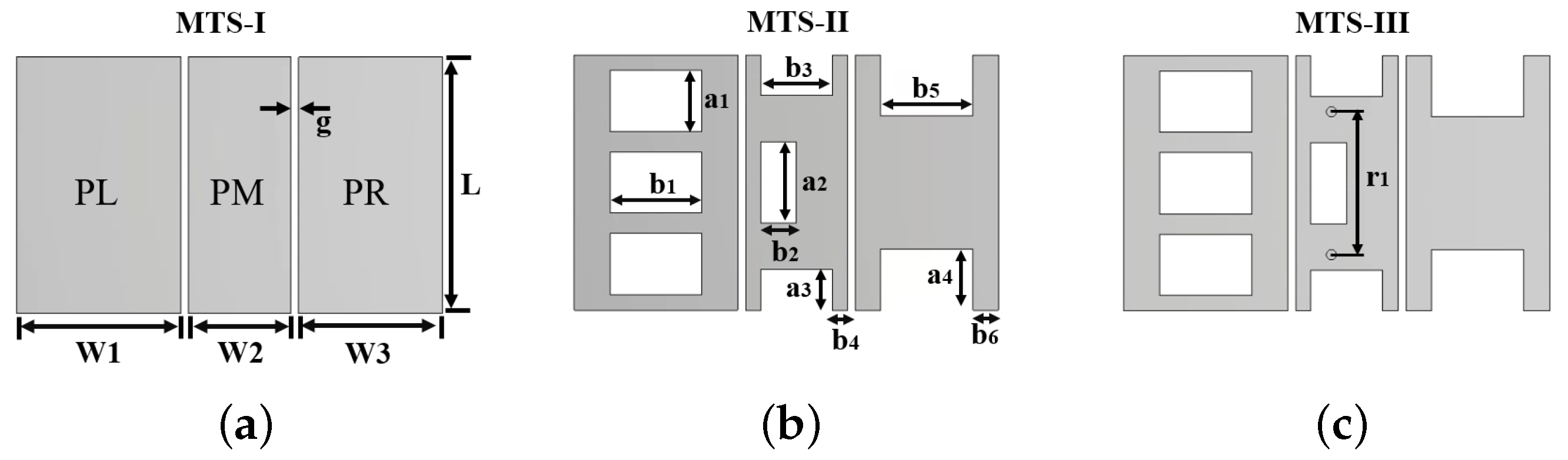
Figure 2.
Illustration of application of PIN diodes in the gaps between sub-patches, and PIN diode model for the State 11 in CMA.
Figure 2.
Illustration of application of PIN diodes in the gaps between sub-patches, and PIN diode model for the State 11 in CMA.
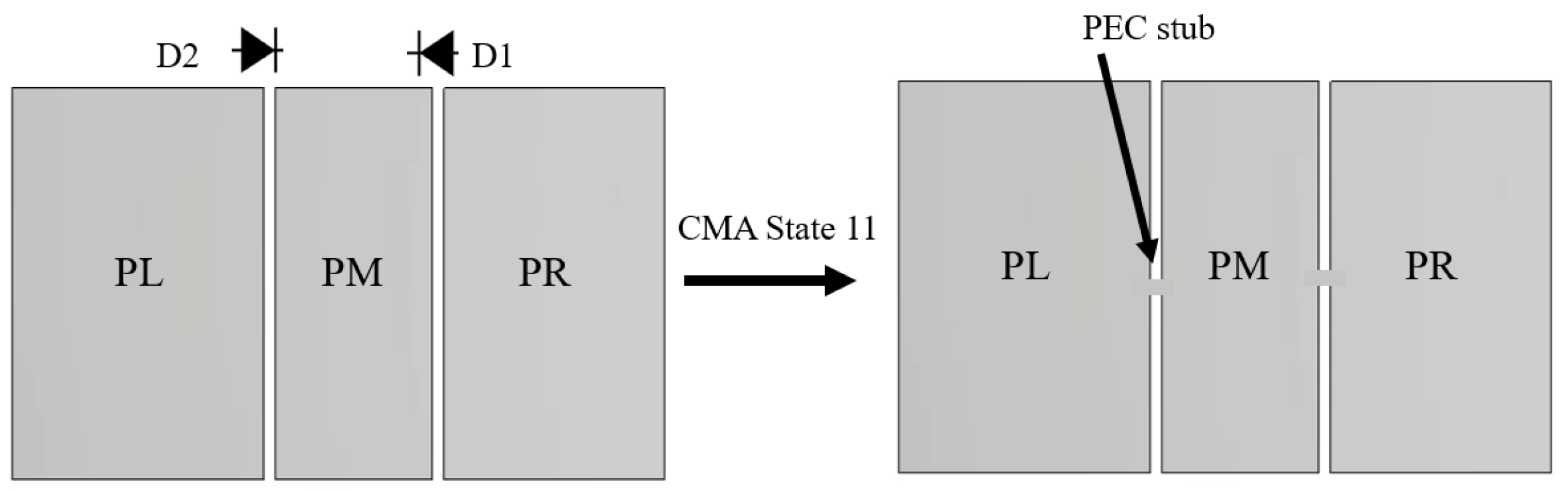
Figure 3.
MS and characteristic angles of MTS-I, Mode 1, and Mode 2 plotted at four different combinations of switching states of PIN diode D1 and D2.
Figure 3.
MS and characteristic angles of MTS-I, Mode 1, and Mode 2 plotted at four different combinations of switching states of PIN diode D1 and D2.
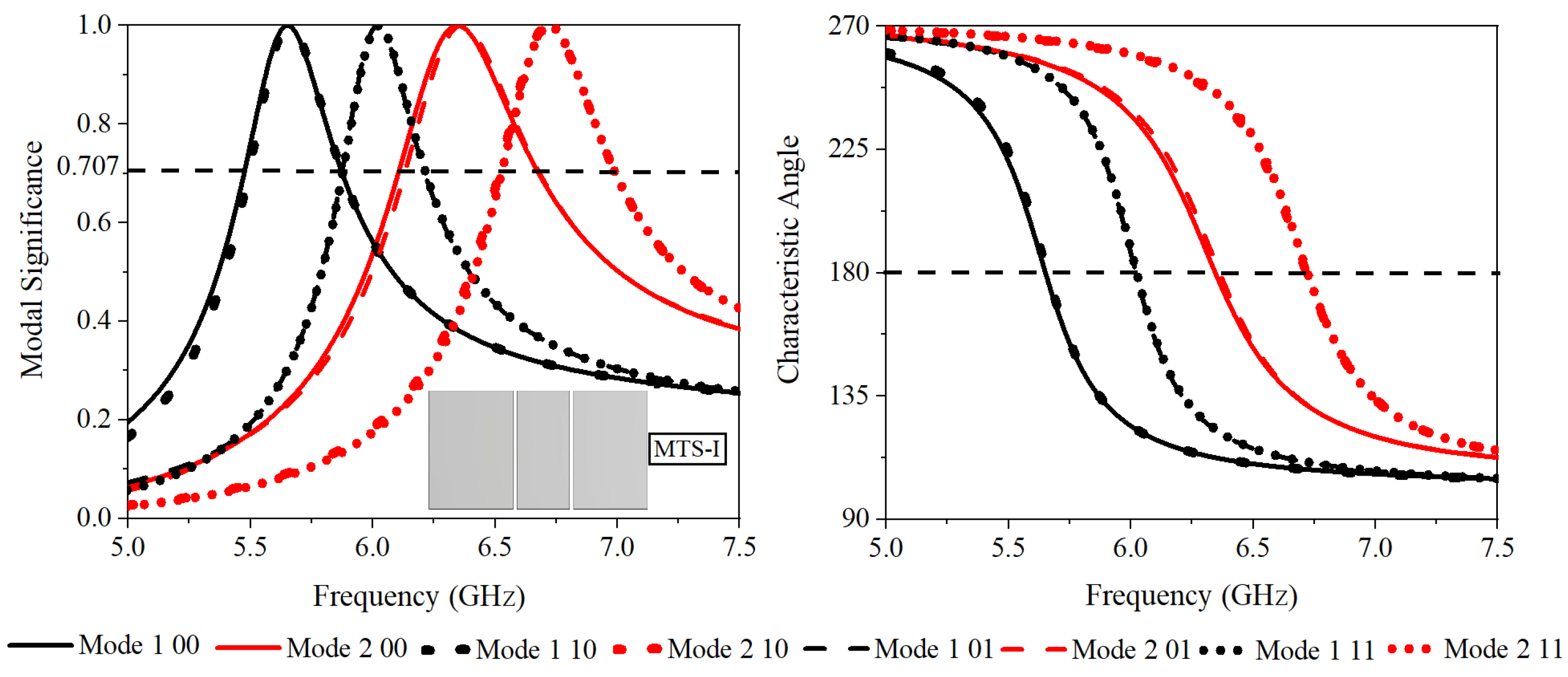
Figure 4.
Modal currents MTS-I (a) Mode 1, (b) Mode 2.
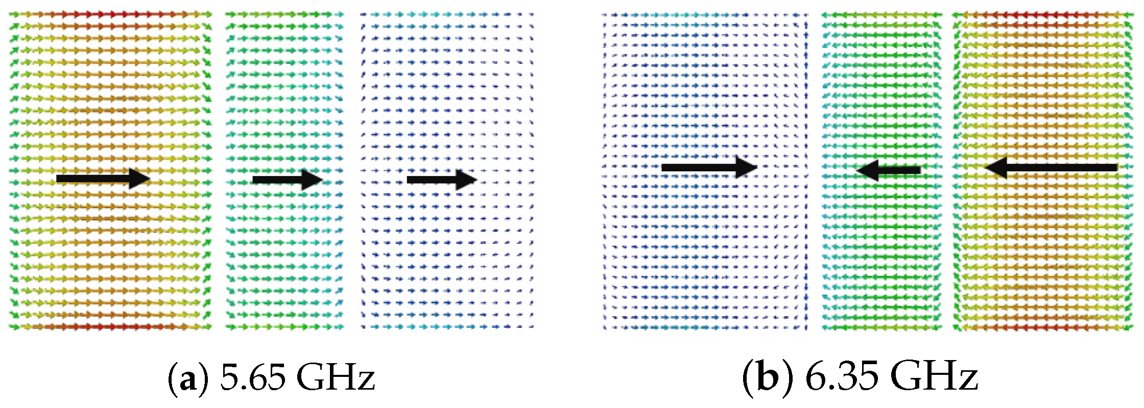
Figure 5.
MS and characteristic angles of MTS-II, Mode 1 and Mode 2 plotted at four different combinations of switching states of PIN diode D1 and D2.
Figure 5.
MS and characteristic angles of MTS-II, Mode 1 and Mode 2 plotted at four different combinations of switching states of PIN diode D1 and D2.
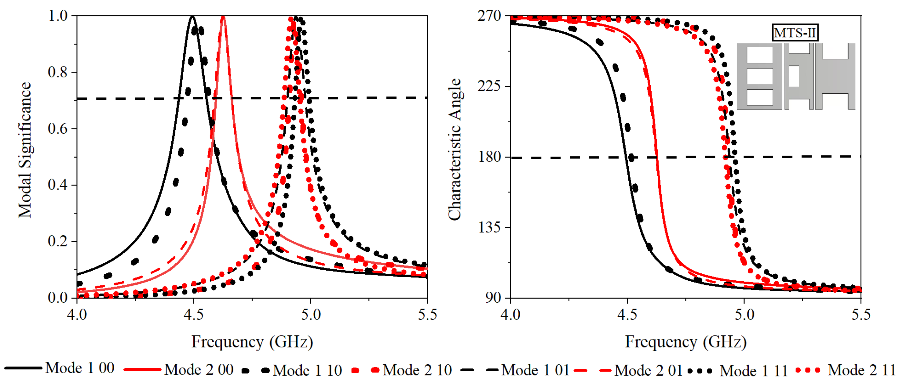
Figure 6.
Modal currents MTS-II (a) Mode 1, (b) Mode 2.
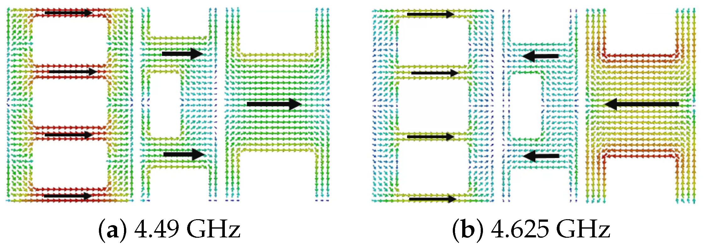
Figure 7.
MS, characteristic angle, and 2-bit phase operation of the proposed unit-cell (MTS-III).
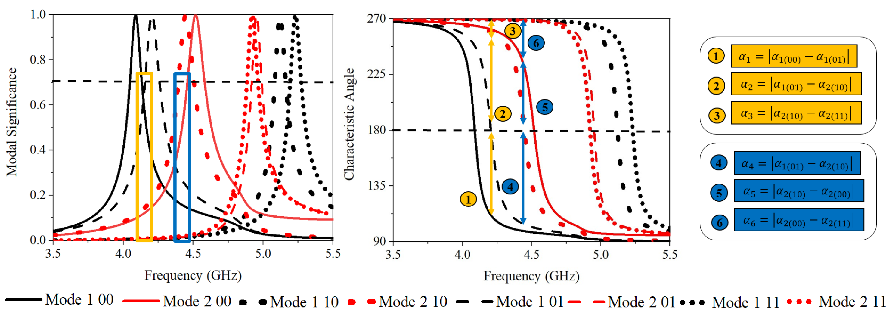
Figure 8.
Modal currents MTS-III (a) Mode 1 at 4.09 GHz, (b) Mode 1 at 4.20 GHz, (c) Mode 2 at 4.45 GHz, (d) Mode 2 at 4.92 GHz, (e) Mode 1 at 4.20 GHz, (f) Mode 2 at 4.45 GHz, (g) Mode 2 at 4.92 GHz, (h) Mode 2 at 4.92 GHz.
Figure 8.
Modal currents MTS-III (a) Mode 1 at 4.09 GHz, (b) Mode 1 at 4.20 GHz, (c) Mode 2 at 4.45 GHz, (d) Mode 2 at 4.92 GHz, (e) Mode 1 at 4.20 GHz, (f) Mode 2 at 4.45 GHz, (g) Mode 2 at 4.92 GHz, (h) Mode 2 at 4.92 GHz.
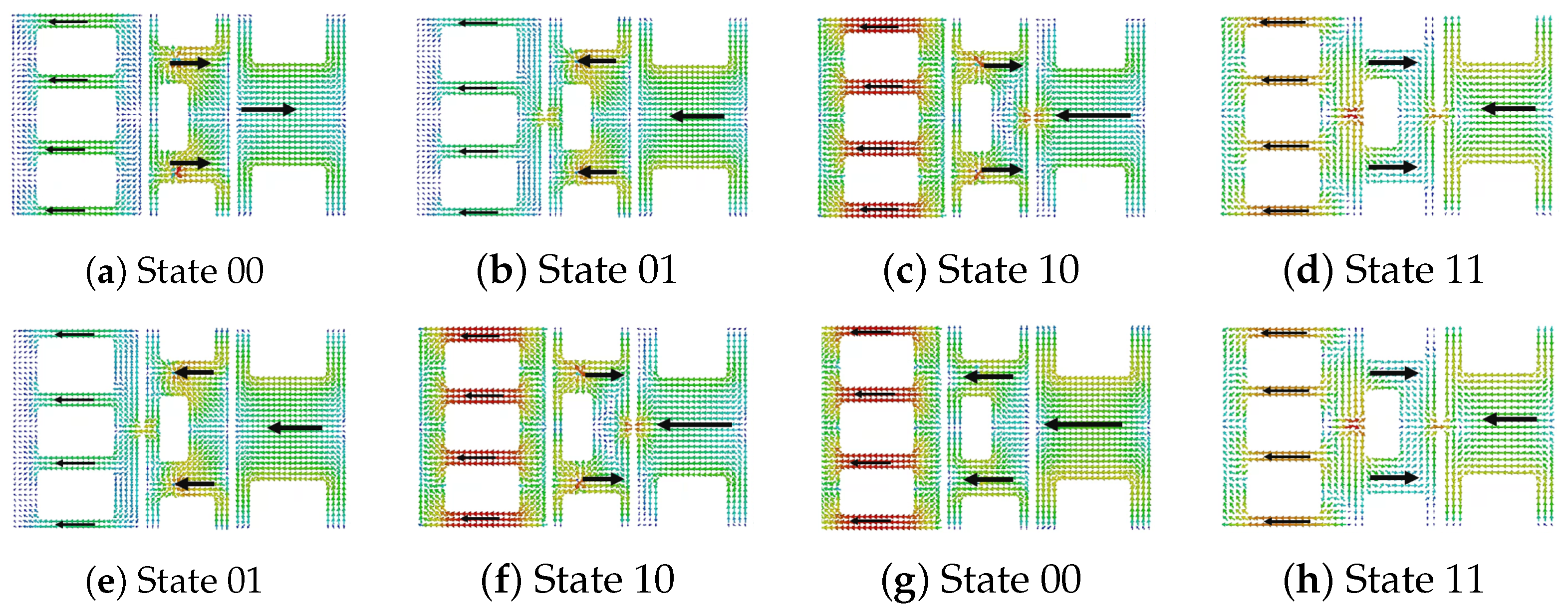
Figure 9.
PIN diode model in unit-cell simulations.

Figure 10.
Simulated reflection coefficients, amplitude, and phase by varying locations of vias moving away from the center of the middle sub-patch. (a) Vx = 1.5 mm, (b) Vx = 1.85 mm (optimum design), (c) Vx = 2.5 mm. The shaded area under the curve highlights the region where MTS-III is providing 2-bit operation.

Table 1.
Dimensions of unit-cell.
| Parameter | W1 | W2 | W3 | L | g | |||
| Size (mm) 1 | 16 | 10 | 14 | 25 | 0.765 | 6 | 8 | 4 |
| Parameter | ||||||||
| Size (mm) 1 | 6 | 9 | 3.5 | 7 | 1.5 | 9 | 2.5 | 7 |
1 Optimized dimensions are provided in the table.
Table 2.
Modeling of PIN diode in CMA.
| PIN Diode | CMA Based Model for PIN Diode |
|---|---|
| OFF State | Disconnected sub-patches |
| ON State | PEC stub in the gap connecting sub-patches |
Table 3.
Size of MTS-I, MTS-II, and MTS-III in both bands.
| Unit-Cell | Resonant Frequency Mode 1 (GHz) | Size * () | Resonant Frequency Mode 2 (GHz) | Size () |
|---|---|---|---|---|
| MTS-I | 5.56 | 6.35 | ||
| MTS-II | 4.49 | 4.625 | ||
| MTS-III | 4.09 | 4.518 |
* Sizes are calculated using the free space wavelength. Modal frequencies are used for the size calculations.
Table 4.
Comparison table.
| Ref [n] | Resonant Frequency | Size * () | Active Components per Unit Cell | Novelty |
|---|---|---|---|---|
| [10] | 6 GHz | 2-pin diodes | Unit-cell design for 2-bit MTS | |
| [11] | 5 GHz | 2-pin diodes, 4-capacitors | Unit-cell design with folded ground plane for 2-bit MTS | |
| [12] | 5.8 GHz | 2-pin diodes | Unit-cell design of2-bit MTS for wireless power transfer | |
| [14] | 9.5 GHz | 2-pin diodes | Time domain digital coding | |
| [17] | 2.3 GHz | 5-pin diodes | Fully functional 2-bit RIS | |
| Current work | 3.915 GHz ** | 2-pin diodes | Unit-cell design for 2-bit MTS using multiple modes in CMA |
* Sizes are calculated using the guided wavelength. ** For the size calculations of MTS-III, the resonant frequency of optimized MTS-III in Section 3 is used.
Disclaimer/Publisher’s Note: The statements, opinions and data contained in all publications are solely those of the individual author(s) and contributor(s) and not of MDPI and/or the editor(s). MDPI and/or the editor(s) disclaim responsibility for any injury to people or property resulting from any ideas, methods, instructions or products referred to in the content. |
© 2023 by the authors. Licensee MDPI, Basel, Switzerland. This article is an open access article distributed under the terms and conditions of the Creative Commons Attribution (CC BY) license (https://creativecommons.org/licenses/by/4.0/).
Share and Cite
MDPI and ACS Style
Fazal, D.; Hong, I.-P. A New Unit-Cell Design for a 2-Bit Reflective Metasurface for RIS Applications. Electronics 2023, 12, 4220. https://doi.org/10.3390/electronics12204220
AMA Style
Fazal D, Hong I-P. A New Unit-Cell Design for a 2-Bit Reflective Metasurface for RIS Applications. Electronics. 2023; 12(20):4220. https://doi.org/10.3390/electronics12204220
Chicago/Turabian StyleFazal, Dilaawaiz, and Ic-Pyo Hong. 2023. "A New Unit-Cell Design for a 2-Bit Reflective Metasurface for RIS Applications" Electronics 12, no. 20: 4220. https://doi.org/10.3390/electronics12204220
Note that from the first issue of 2016, this journal uses article numbers instead of page numbers. See further details here.