Article

Output Waveform Distortion Suppression Method of Asymmetric Sine Wave Inverter Based on Online Identification and Linearization of System Transmission Characteristics

1
School of Electrical Engineering and Automation, Harbin Institute of Technology, Harbin 150001, China
2
State Grid Harbin Power Supply Company, Harbin 150001, China
3
School of Mechanical and Electrical Engineering, Heilongjiang University, Harbin 150080, China
*
Author to whom correspondence should be addressed.
Electronics 2023, 12(20), 4279; https://doi.org/10.3390/electronics12204279
Submission received: 19 September 2023 / Revised: 7 October 2023 / Accepted: 15 October 2023 / Published: 16 October 2023
(This article belongs to the Section Power Electronics)

Abstract

:
Limited by the switching frequency of an insulated gate bipolar transistor (IGBT), the system bandwidth of high-power inverters is low. If the amplitude and phase changes of each harmonic from the reference signal to the output waveform are defined as transmission characteristics, it can be concluded that the limited bandwidth will result in nonlinear system transmission characteristics. This results in the amplitude and phase distortion of each harmonic of the asymmetric sine wave, which in turn leads to severe distortion of the output waveform. Therefore, this article proposes a method to linearize transmission characteristics. This method effectively offsets the nonlinear effect of transmission characteristics, which is caused by the limited bandwidth, by causing distortions with respect to each harmonic in the reference signal, thereby suppressing the distortion of the output waveform. In addition, an online identification method of transmission characteristics based on a state observer is proposed to achieve the online linearization of system transmission characteristics. This method does not rely on closed-loop system control, has no stability problems, and can be used for a variety of control methods. Simulation and experiments verify the effectiveness of this method.

1. Introduction

Micro-arc oxidation can greatly enhance the corrosion resistance, wear resistance, and other properties of nonferrous metals, and it is therefore widely used in industrial, medical, and aerospace fields [1,2]. The current micro-arc oxidation power supply usually adopts an asymmetrical rectangular pulse waveform, and the capacitive characteristics of the load can cause transistor voltage and current spikes [3]. This can increase the electrical stress on the transistor, which in turn can reduce the reliability of the device.
To solve the above problems, the asymmetric sinusoidal output waveform shown in Figure 1 is proposed as a power supply for micro-arc oxidation. Asymmetric sine wave micro-arc oxidation power supplies require a wide range of adjustable output frequencies (typically 50 Hz–1 kHz) and adjustable positive and negative half-cycle amplitudes. Since asymmetric sine waves have high fundamental frequencies and abundant harmonics, closed-loop systems usually need to have high bandwidth and excellent control performance to ensure that the amplitude and phase distortion of each harmonic component is minimized in order to ensure the quality of the output waveform.
Inverters are widely used in microgrid systems [4,5], electric drives, and other fields; thus, the suppression of output waveform distortions is a typical problem and has been widely studied. To reduce inverter output waveform distortions, many control methods have been proposed and have achieved good results in sine wave systems, such as proportional integral control (PI), proportional resonance control (PR), repetitive control (RC), model predictive control (MPC), sliding mode control (SMC), and deadbeat control (DBC) [6,7,8,9,10,11]. PI control is the easiest to implement, but since it cannot achieve steady-state errors for asymmetric sinusoidal waves according to the internal mode theorem, the effect of suppressing waveform distortion is limited. PR and RC can provide high gains at harmonic frequency points and, therefore, can effectively suppress harmonics in the output waveform. However, asymmetric sinusoidal waveforms need to control the amplitude and phase of each harmonic without distortion rather than eliminating them; thus, it is not suitable for asymmetric sine waves. MPC, SMC, and DBC have the ability to achieve better output waveform quality in asymmetric sine wave systems. However, since the usual switching frequency of IGBT is lower than 20 kHz, according to the sampling law [12], the system bandwidth cannot be higher than half of the switching frequency. The limited bandwidth causes distortions with respect to each harmonic, resulting in the severe distortion of the output waveform. Therefore, these methods are powerless with respect to asymmetric sine waves, which have high fundamental frequencies and rich harmonics. Particularly for MPC, in order to limit the maximum switching frequency, its equivalent switching frequency will be lower than 20 kHz, and it will be more difficult to suppress waveform distortions.
There are also some studies on reducing output waveform distortions. The authors reduced waveform distortions by injecting third harmonics in Refs. [13,14,15], but the asymmetric sine wave itself is rich in harmonics and is unsuitable for this method. The authors in [16] utilized two zero common-mode voltage vectors and a virtual vector, which are a combination of two other vectors with equal duty cycles, to minimize output waveform distortions. A method for the real-time calculation of optimal switching angles for step modulation was proposed in Ref. [17] to minimize waveform distortion. The authors also used modulation to reduce output waveform distortion in Refs. [18,19]. However, the distortion of asymmetric sine waves mainly comes from the limited bandwidth of the output filter and closed-loop control. Even if all effects related to the modulation part are eliminated, the problems caused by the limited bandwidth still cannot be solved.
In addition, the output waveform distortion can be reduced by fitting the output waveform with more output levels. A method using 24 H-bridge inverters that were cascaded to generate 49 levels was proposed in Ref. [20] to generate arbitrary waveforms, achieving high-voltage and high-frequency output. Multi-pulse converters can also be combined with inverters to achieve multi-level output structures [21]. Flying capacitor inverters can achieve more output levels at higher power densities [22]. In Ref. [23], the author proposed a method of combining the H4 inverter and H6 inverter, allowing them to provide a quasi-square wave and seven-level combination to generate nineteen levels, respectively, which can realize multiple levels with lower devices. Although these methods can effectively reduce output waveform distortions, the structure is too complex, and cost, volume, and reliability limit their practical application.
The limited bandwidth mainly affects the output waveform distortion of the asymmetric sine wave inverter, but the switching frequency determines that any closed-loop control method cannot break through the upper limit of the bandwidth. In order to solve the above problems, the amplitude and phase changes of each harmonic component from the reference signal to the output waveform are defined as transmission characteristics, and a linearization method of transmission characteristics is proposed. There is no need for complex topology and control methods, and output waveform distortions can effectively be reduced by modifying the reference signal. Even the simplest H-bridge inverter and the simplest PI control can achieve high-quality output waveforms.
The rest of this paper is organized as follows: Section 2 analyzes the reasons for output waveform distortion caused by limited bandwidth, defines the transmission characteristics of the system, and proposes a linearization method for transmission characteristics. An online identification method of transmission characteristics based on state observer is proposed in Section 3. Simulations and experiments verify the effectiveness of the proposed method in Section 4. Finally, Section 5 concludes the paper.

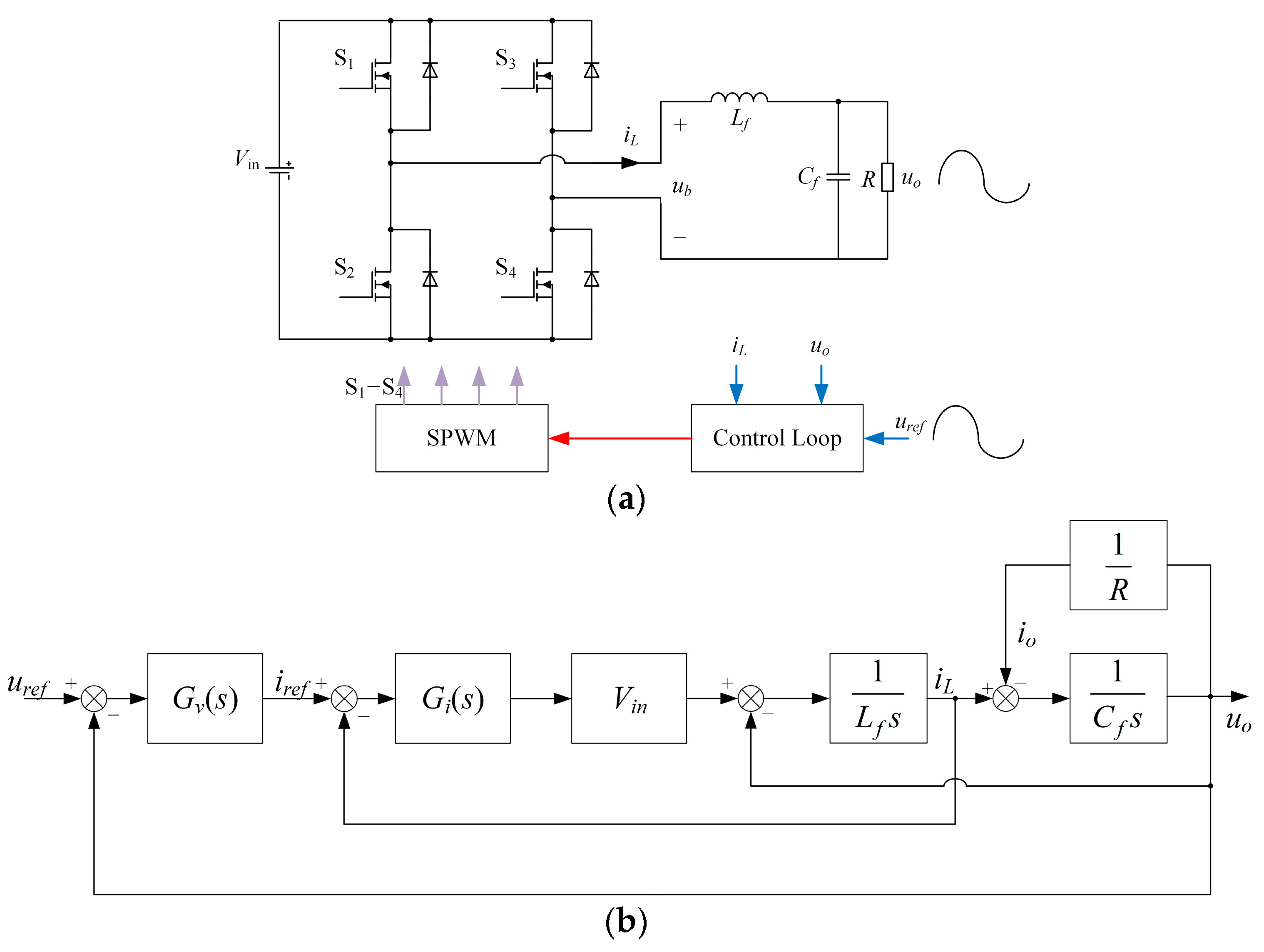
2. Output Waveform Distortion Mechanism and the Linearization of Transmission Characteristics

2.1. Output Waveform Distortion Mechanism and Transmission Characteristics

For an asymmetric sinusoidal signal, such as that shown in Figure 1, in order to facilitate analysis, its Fourier series can be expressed as:
u ( t ) = P N π + P + N 2 sin ω u o t k = 1 2 ( P N ) π ( 4 k 2 1 ) cos ( 2 k 2 π f u o t )
where P represents the amplitude of the positive half cycle, N represents the amplitude of the negative half cycle, and f u o is the fundamental frequency. According to Equation (1), the asymmetric sine wave contains not only the DC components, fundamental wave, and the first harmonic but also all even harmonics. In addition, when the amplitude of the negative half cycle is 0, the amplitude of each even harmonic component reaches the maximum; thus, the worst working condition occurs when the amplitude of the negative half cycle is 0. This paper takes this situation as an example of verification.
The H-bridge inverter structure shown in Figure 2a is used to generate asymmetric sine waves. Taking the double-loop PI control shown in Figure 2b as an example, the transfer function from the reference signal to the output voltage can be expressed as follows:
G s ( s ) = u o ( s ) u r e f ( s ) = R G v ( s ) G i ( s ) V i n R L f C f s 2 + R C f G i ( s ) V i n s + R G v ( s ) G i ( s ) V i n + R + L f s + G i ( s ) V i n
where S1S4 is the transistor and its driving signal, uo is the output voltage, uref is reference voltage, Lf is the filter inductor, Cf is the filter capacitor, iL is inductor current, Vin is the input bus voltage, R is the load resistance, Gv(s) represents the PI transfer function of the voltage loop, and Gi(s) represents the PI transfer function of the current loop.
Since the reference signal consists of DC components and harmonics, it can be expressed as follows:
u r e f ( t ) = A r d c + A r n sin ( n 2 π f u o t + φ n ) = u r e f ( f n )
where n represents the harmonic order, f n = n f u o represents the frequency of the harmonic, uref(fn) represents the component of uref at each harmonic frequency, Ar−dc represents the dc component, Ar−n represents the amplitude of each harmonic, and φn represents the phase of each harmonic. According to Equations (2) and (3), the expression of the output waveform can be described as follows:
u o ( t ) = f ( 0 ) A r d c + f ( f n ) A r n sin ( n 2 π f u o t + φ n g ( f n ) )
where f(fn) represents the amplitude gain of G s j 2 π f n at harmonic frequency f n , and g(fn) represents the phase attenuation of G s j 2 π f n at harmonic frequency f n .
Since the curve of the amplitude and phase of G s j 2 π f n , which changes with frequency, is not a horizontal straight line, distortions in amplitude and phase occur at each harmonic. The distortion of each harmonic eventually causes the output waveform to be distorted. Figure 3 illustrates how this distortion works.
Since both the output waveform and the reference signal are composed of a limited number of harmonic components, generally, the harmonic components of the output waveform are only affected by the corresponding harmonics of the reference signal. Therefore, the harmonic components of the output waveform can be viewed as being mapped from the harmonic components of the reference signal. This mapping is called the transfer characteristic, which is actually equivalent to the discretization of transfer function G s s . According to Figure 3, the transmission characteristic of the system is nonlinear, which causes harmonic distortions of each order, and these can be expressed as follows:
u r e f ( f n ) { f , g } ( f n ) u o ( f n )

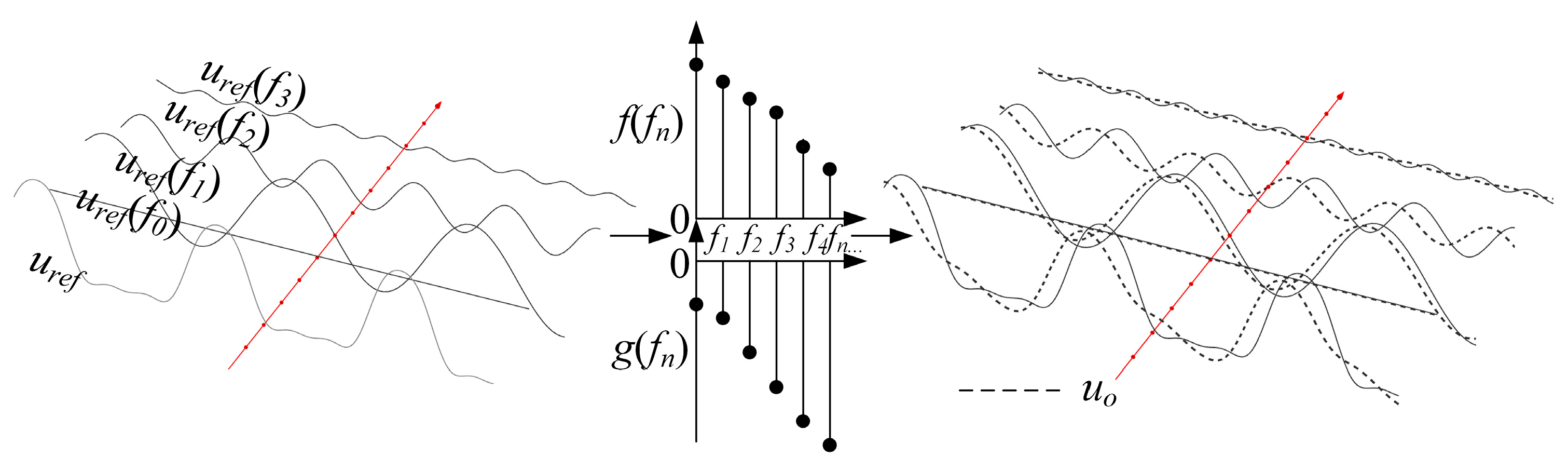
2.2. Linearization of Transmission Characteristics

According to Equation (2), a method to suppress output waveform distortion can be easily obtained, which is expressed as follows:
u o ( s ) = G s 1 ( s ) ( G s ( s ) u r e f ( s ) ) = u r e f ( s )
Obviously, by adding G s 1 s to the control loop, the effect of G s s can be offset so that the output waveform is completely equal to the reference signal, eliminating the distortion of the output waveform caused by the limited bandwidth. G s 1 s must be expressed as follows:
G s 1 ( s ) = b m s m + b m 1 s m 1 + b m 2 s m 2 + + b 0 a n s n + a n 1 s n 1 + a n 2 s n 2 + + a 0
However, due to the physical characteristics of the actual system, the order of the numerator and denominator in G s 1 s must satisfy m > n . This is an unstable system and can easily diverge. Although stability can be ensured by cascading low-pass filter stages in theory, to meet stability, the bandwidth of G s 1 s needs to be significantly reduced, thus losing the compensation effect.
Since the transmission characteristics of the system are the mapping relationship between discrete harmonic components and harmonic components, which is a mathematical relationship rather than a physical structure, there is no stability problem. Then, the compensation relationship of Equation (6) is equivalent to the composition of the mapping relationship. This process can be expressed as follows:
u r e f ( f n ) { f 1 , g 1 } ( f n ) u m ( f n ) { f , g } ( f n ) u o ( f n )
where um is the generated intermediate signal, which is used as a new reference signal for the actual closed-loop control system, and f 1 and g 1 are the inverse mappings corresponding to f and g, respectively. According to the definitions of f and g, f 1 and g 1 satisfy the following:
f 1 f = 1 , g 1 + g = 0
This method shown in Equation (8) is the linearization of the transmission characteristics. Figure 4 takes Figure 2b as an example to show the actual structure of the linearization of transmission characteristics. Since the transmission characteristic linearization method actually generates an intermediate signal by modifying the reference signal, it does not involve the closed-loop control part of the system and remains unaffected regardless of whether the system operates in a closed loop or an open loop, so it does not affect the stability of the system itself.
An example is given to facilitate the understanding of the linearization process of transmission characteristics. We assume a reference signal; then, the corresponding transmission characteristics and the corresponding output signal are as follows:
u r e f e = 0.5 sin ( 2 π f 1 ) + 0.7 sin ( 2 π f 2 ) f ( f 1 ) = 0.9 , g ( f 1 ) = 0.3 π , f ( f 2 ) = 0.7 , g ( f 2 ) = 0.5 π u o e = 0.45 sin ( 2 π f 0.3 π 1 ) + 0.49 sin ( 2 π f 2 0.5 π )
It is obvious that uoe is distorted relative to urefe. Combining Equations (8)–(10), intermediate signal ume and linearized uoe are described as follows:
f 1 ( f 1 ) = 1.11 , g 1 ( f 1 ) = 0.3 π , f 1 ( f 2 ) = 1.43 , g 1 ( f 2 ) = 0.5 π u m e = 0.56 sin ( 2 π f 1 + 0.3 π 1 ) + 1 sin ( 2 π f 2 + 0.5 π ) u o e = 0.5 sin ( 2 π f 1 ) + 0.7 sin ( 2 π f 2 ) = u r e f e
After the transmission characteristics are linearized, the output signal can completely track the reference signal such that the system’s output waveform is not affected by the system bandwidth. Since the transfer characteristic linearization method relies on the inverse of the system’s transfer characteristics, the system’s transfer characteristics changes with the input DC voltage, filter parameters, and load. In this way, the key to suppressing output waveform distortions lies in identifying the inverse of the system’s online transmission characteristics.

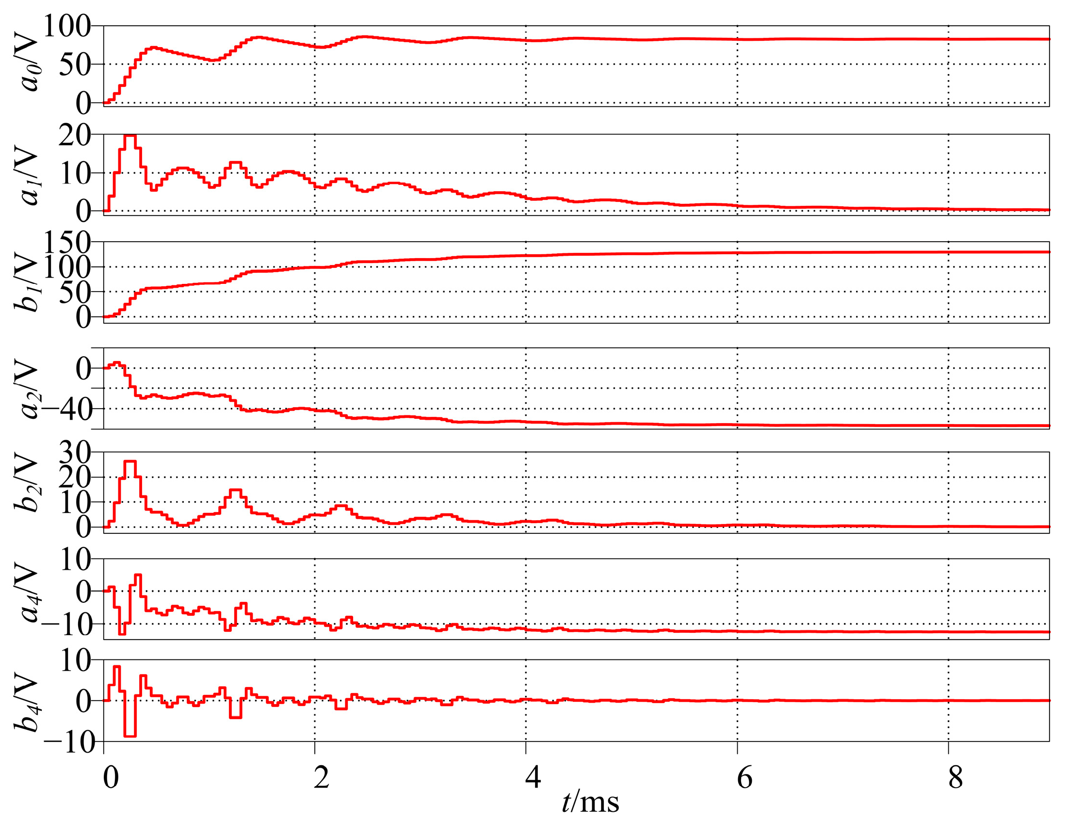
3. Online Identification Method of Transmission Characteristics Based on the State Observer

For any periodic signal, it can be expressed as follows:
u o ( t ) = a 0 + a n cos ( n 2 π f u o ) + b n sin ( n 2 π f u o )
The selected state variables are x 1 , a 0 , a 1 , b 1 , a 2 , b 2 , etc., where x 1 ˙ = u o t . Moreover, the output variable is selected as y = u o t ; then, the Fourier series form of the signal can be expressed as a state equation:
( x 1 · a 0 · a 1 · b 1 · ) = ( 0 1 cos ( 2 π f u o ) sin ( 2 π f u o ) 0 0 0 0 0 0 0 0 0 0 0 0 0 0 0 0 0 0 0 0 ) ( x 1 a 0 a 1 b 1 ) y = ( 0 1 cos ( 2 π f u o ) sin ( 2 π f u o ) ) ( x 1 a 0 a 1 b 1 )
Equation (13) can be abbreviated as follows:
x · = A x y = C x
Therefore, a virtual system can be constructed and error feedback can be introduced to obtain the following:
x ^ · = A x ^ + L ( y y ^ ) y ^ = C x ^
where x ^ and y ^ are the estimated values of x and y , respectively, and L is the gain matrix, according to the following relationship:
x ^ · x · = A x ^ A x + L ( y y ^ ) = ( A L C ) ( x x ^ )
Therefore, if matrix A L C is not positive definite, then lim x ^ x = 0 . In this way, state variable x can be estimated via the virtual system and actual output y . Since matrix L is a column vector and the first columns of matrices C and A are both 0, the first column of matrix A L C is also 0, and the value of determinant A L C must also be 0. Since matrix A L C is not positive definite, the trace of matrix t r ( A L C ) must also be less than 0. If the following is defined:
L = ( l 0 l 1 l 2 l 3 ) T
then A L C can be expressed as follows:
A L C = ( 0 1 l 0 ( 1 l 0 ) cos ( 2 π f u o t ) ( 1 l 1 ) sin ( 2 π f u o t ) 0 l 1 l 1 cos ( 2 π f u o t ) l 1 sin ( 2 π f u o t ) 0 l 2 l 2 cos ( 2 π f u o t ) l 2 sin ( 2 π f u o t ) 0 l 3 l 3 cos ( 2 π f u o t ) l 3 sin ( 2 π f u o t ) )
Then, the trace of A L C can be expressed as follows:
t r ( A L C ) = l 1 l 2 cos ( 2 π f u o t ) l 3 sin ( 2 π f u o t ) l 4 cos ( 2 2 π f u o t )
Obviously, the selected parameters are as follows:
l 1 = l a 0 , l 2 = l a 1 cos ( 2 π f u o t ) , l 3 = l b 1 sin ( 2 π f u o t ) , l 4 = l a 2 cos ( 2 2 π f u o t ) ,
As long as l a n and l b n are selected to be greater than 0, the following can be satisfied:
t r ( A L C ) = l a 0 l a 1 cos 2 ( 2 π f u o t ) l b 1 sin 2 ( 2 π f u o t ) l a 2 cos 2 ( 2 2 π f u o t ) < 0
Therefore, the virtual system (15) must converge to lim x ^ = x so that the coefficients in the Fourier series form of the output voltage waveform can be observed online. Parameters l a n and l b n , respectively, determine the convergence speed of each coefficient in the observation. Since the virtual system shown in Equation (15) is in the time domain and the microprocessor can only process discretized signals, Equation (15) needs to be discretized. Bringing x ^ into y ^ , Equation (15) can be written as follows:
x ^ · = ( A L C ) x ^ + L y
According to the relationship between differentiation and difference, when the discrete time interval is Δ t , Equation (22) is described as follows:
x ^ k + 1 = x ^ k + ( ( A L C ) x ^ k + L y k ) Δ t = ( I + Δ t A Δ t L C ) x ^ k + Δ t L y k = A k x ^ k + L k y k
where
A k = ( 1 Δ t ( 1 l 0 ) Δ t ( 1 l 0 ) cos ( 2 π f u o t ) Δ t ( 1 l 0 ) sin ( 2 π f u o t ) 0 1 Δ t l 1 Δ t l 1 cos ( 2 π f u o t ) Δ t l 1 sin ( 2 π f u o t ) 0 Δ t l 2 1 Δ t l 2 cos ( 2 π f u o t ) Δ t l 2 sin ( 2 π f u o t ) 0 Δ t l 3 Δ t l 3 cos ( 2 π f u o t ) 1 Δ t l 3 sin ( 2 π f u o t ) ) L k = ( Δ t l 0 Δ t l 1 Δ t l 2 Δ t l 3 ) T
Therefore, the coefficients in the Fourier series can be expressed as follows:
a 0 , k + 1 = a 0 , k ( 1 Δ t l 1 ) Δ t l 1 ( a 1 , k cos ( 2 π f u o t ) + b 1 , k sin ( 2 π f u o t ) + ) + Δ t l 1 y a 1 , k + 1 = a 1 , k ( 1 Δ t l 2 cos ( 2 π f u o t ) ) Δ t l 2 ( a 0 , k + b 1 , k sin ( 2 π f u o t ) + ) + Δ t l 2 y
To simplify representation and calculation, we define the following:
S k = a 0 , k + a 1 , k cos ( 2 π f u o t ) + b 1 , k sin ( 2 π f u o t ) + a 2 , k cos ( 2 2 π f u o t ) +
Then, Equation (25) can be expressed as follows:
a 0 , k + 1 = a 0 , k + Δ t l 1 ( y S k ) a 1 , k + 1 = a 1 , k + Δ t l 2 ( y S k )
Combining Equations (20) and (27), the coefficients in the Fourier series of the output waveform can be estimated. Then, according to the trigonometric function relationship, the amplitude and phase of each harmonic component can be obtained; then, the transmission characteristics of the system and its inverse can be obtained. In the method of obtaining coefficients in the Fourier series based on the observer, different transient processes will result from different gains in gain matrix L . In order to ensure the accuracy of transmission characteristic identification, it is necessary to determine whether the observer has reached a steady state. The simplest way to judge the steady state is to compare the observation results for every j sampling period. Since the first two harmonic components account for a high proportion, if the error of the coefficients of the first two adjacent harmonics is less than a certain value, the system is considered to have reached a steady state, and the value of j can be selected based on actual conditions.
According to the analysis in Section 2 and Section 3, the complete process of linearizing transmission characteristics online is shown in Figure 5. At the beginning of the operation, uref is directly sent to the control system as um; then, the output voltage waveform is continuously sampled, and the transmission characteristics are identified. When the observer reaches a steady state, the harmonic information of the output waveform is obtained; then, the transmission characteristics of the system are calculated. Based on the harmonic information of um generated in the previous linearization cycle, the harmonics of um in this cycle are calculated, and um is generated and sent to the control system.
In addition, it is worth noting that due to the computing power of the microprocessor, to calculate the entire operation process within Δ t , Δ t cannot be too small. For high-order harmonics, too large Δ t will lead to insufficient sampling points in each high-order harmonic cycle, which will affect the calculation accuracy. Therefore, Δ t must be determined based on the computing power of the microprocessor and the harmonic frequency that needs to be identified. If the computing power of the microprocessor is insufficient, it will not be able to accurately identify higher frequency harmonic components.

4. Simulation and Experimental Verification

The simulation and experimental parameters are shown in Table 1.

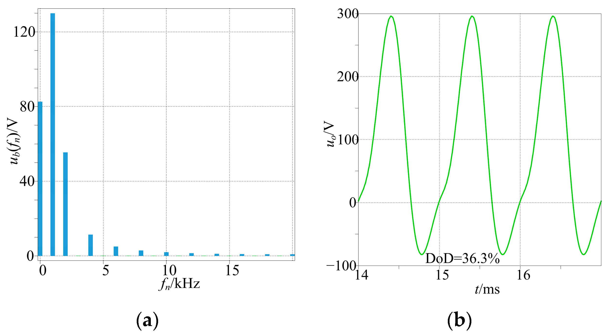
4.1. Simulation Verification

A simulation platform was built in the PLECS 4.5.6 software, and the proposed observer-based harmonic estimation method was verified. The online estimation of the asymmetric sine wave reference signal was performed. The first three harmonics were taken as an example. The real-time estimation results are shown in Figure 6. Since the first three harmonics of the asymmetric sine wave are the fundamental wave and the second and fourth harmonic, the subscripts of the coefficients of the Fourier series are 1, 2, and 4, respectively, and a0 represents the DC component.
Figure 6 shows that the observer can obtain the coefficients of the Fourier series of the reference signal after the transient process. The amplitude and phase information of the first three harmonics and DC components obtained based on various coefficients and their theoretical values are compared in Table 2. As the harmonic frequency increases, the ratio of the observer’s execution frequency to the harmonic frequency decreases, and it is difficult for the observer to reproduce the harmonic information; thus, the error increases, but it can still meet the needs of use. Table 2 shows that the proposed method can effectively obtain the harmonic information of the measured waveform online, which can ensure that online transmission characteristic identification can be realized.
In order to verify the principle of asymmetric sine wave inverter output waveform distortions, Figure 7a shows the spectrum diagram of bridge output waveform ub (shown in Figure 2a), which was generated using the method discussed in Ref. [18]. Figure 7a shows that the spectrum of the waveform before the filter is exactly the same as the theoretical value of the asymmetric sine wave, but the output waveform shown in Figure 7b still has obvious distortions. This is because the output filter causes nonlinearity in the transmission characteristics of the system, and each harmonic component is distorted. To identify the waveform quality of asymmetric sine waves, the degree of distortion (DoD) is introduced as an evaluation index, as follows:
DoD = 0 T o ( u r e f u o ) 2 d t 0 T o u r e f 2 d t × 100 %
where T o is the period of the output waveform. A smaller DOD represents a smaller difference between the output waveform and the desired waveform, which reflects a higher quality.
In order to further verify that the output waveform distortion of the asymmetric sine wave inverter comes from the limited bandwidth of the system in the closed-loop control system, Figure 8 shows the output voltage waveform under SMC. SMC can provide higher bandwidths. Higher system bandwidths result in lower nonlinearity of transmission characteristics; thus, the output waveform distortion is significantly reduced. However, limited by the switching frequency, the system bandwidth is limited; thus, the output waveform is still distorted.
Figure 9 shows the output voltage waveform using the proposed linearization of the transfer characteristics. In order to fully demonstrate the effect of the proposed method, the system adopts open-loop control at this time, that is, intermediate signal um generated by the linearization of the transmission characteristics directly generates a Pulse-Width Modulation (PWM) signal through the modulator. Although the system is under open-loop control, the system’s bandwidth is lower, and the impact of the filter is more serious; the proposed method effectively linearizes the system’s transmission characteristics, and the output waveform shows a lower degree of distortion.

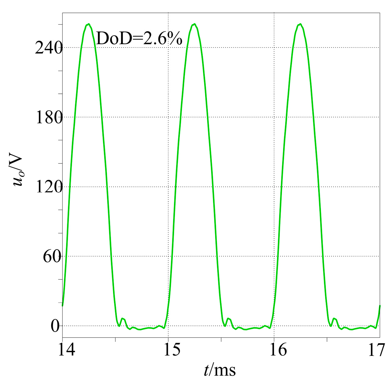
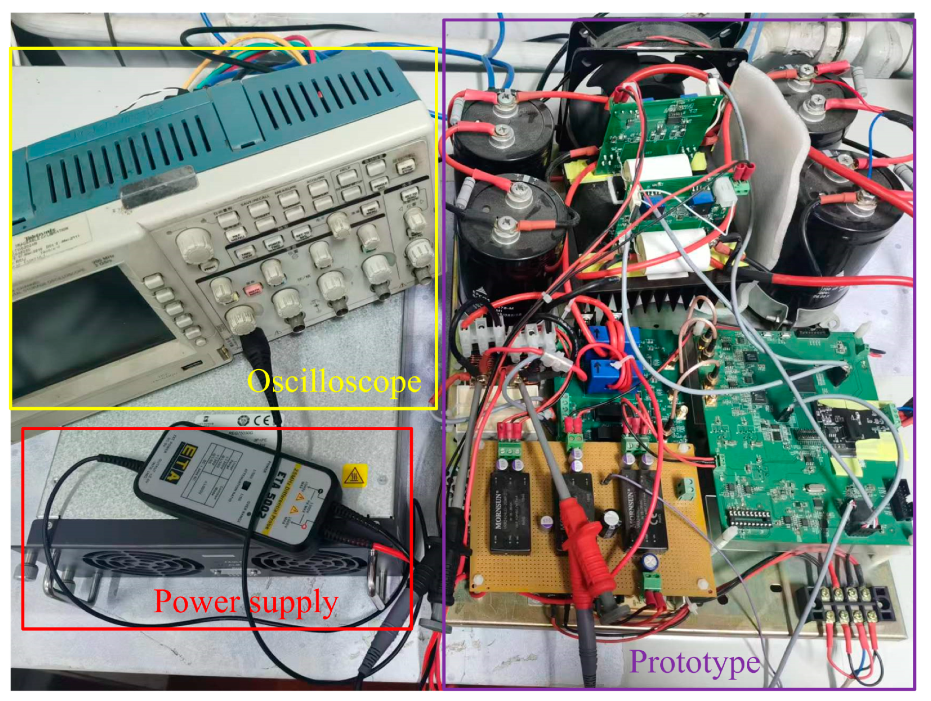
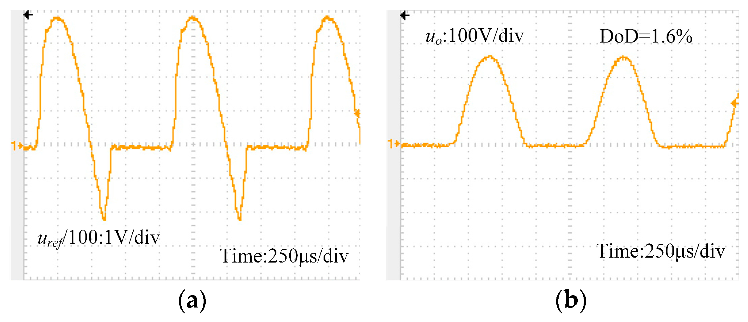
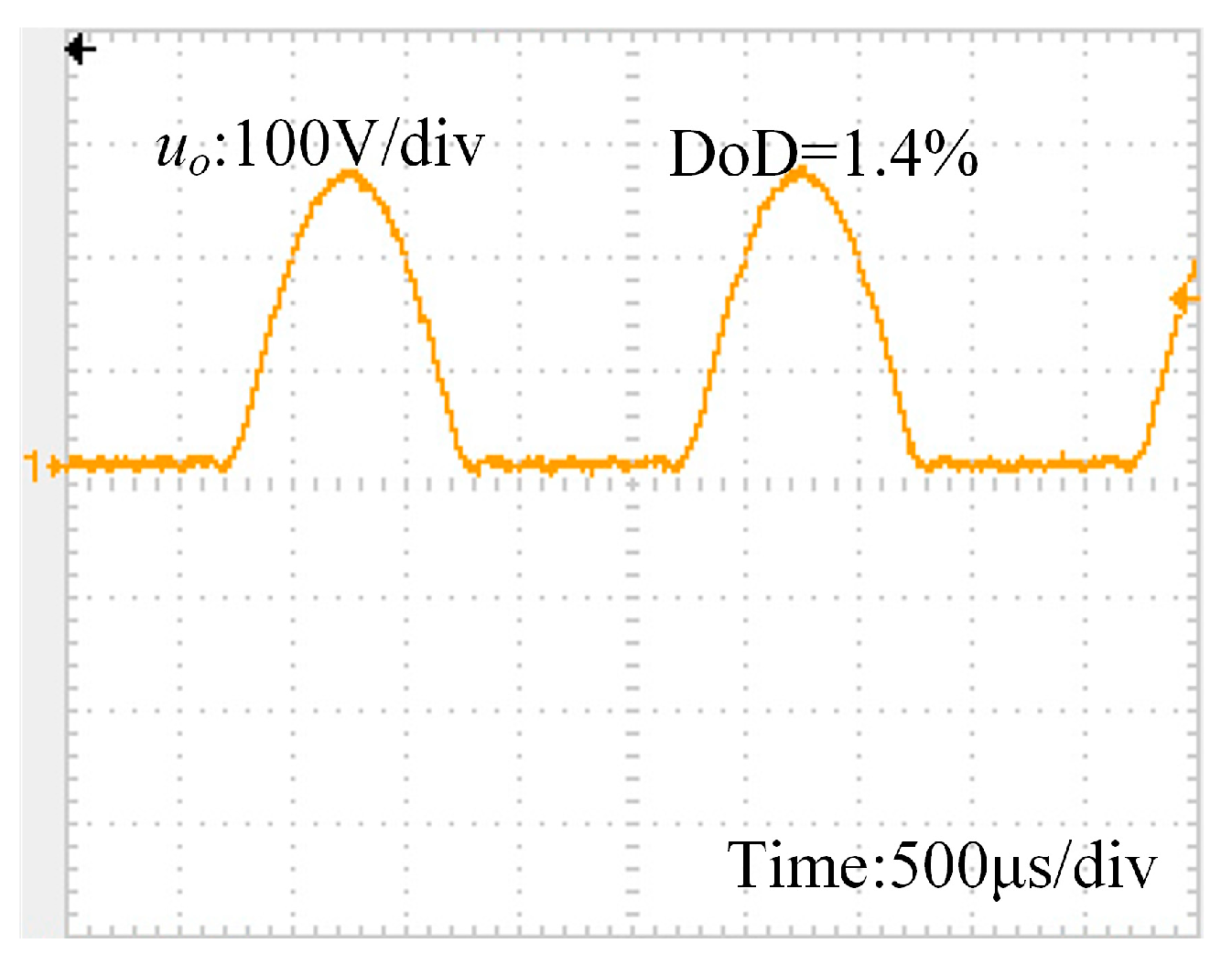
4.2. Experimental Verification

The experimental prototype is shown in Figure 10. The IGBT of Infineon’s IKQ40N120CT2 was selected as the power switch, and the dead time was set to 1 μs. Although it was verified in the simulation that the proposed method combined with open-loop control can effectively reduce the output waveform distortion, considering issues such as system stability and anti-disturbance ability, most systems work in a closed loop; thus, the experimental verification is based on the structure shown in Figure 4. The current loop controller is G i z = 0.1 , and the voltage loop controller is G v z = 0.04 + 0.02 / z 1 . The first six harmonics, that is, the harmonic frequencies of 1 kHz−10 kHz, participate in the linearization of transmission characteristics.
The experimental test is divided into three stages. Stage 1 is the initial operation stage of the converter, and no transmission characteristic linearization method is involved. Stage 2 starts the transmission characteristic linearization method to suppress the output waveform distortion. Stage 3 is when the load is switched from full load to half load (i.e., 60 Ω). Since the system needs a certain amount of time to identify the system’s transmission characteristics, there will be a period of output waveform distortion. After the system transmission characteristics identification is completed, stage 4 begins, which is similar to stage 2. In order to better demonstrate this process, the waveforms of the output voltage and current of the above process on a long time scale are shown in Figure 11.
Intermediate signal um and the output voltage waveform of stage 1 are shown in Figure 12. The reference signal is output by DAC. Although the intermediate signal as the given signal of the closed-loop control system is a standard asymmetric sine wave, due to the limited bandwidth of the control system, amplitude and phase distortion occur at each harmonic. Therefore, the output waveform is obviously distorted, and the amplitude cannot reach the rated value, resulting in a DoD as high as 6.7%.
The intermediate signal and output voltage waveforms of stage 2 are shown in Figure 13. Due to the involvement of the transmission characteristic linearization method, the intermediate signal is no longer a standard asymmetric sine wave but a waveform in which each harmonic is distorted. However, since these distortions offset the effect of the system’s transmission characteristics, the distortion of the output voltage waveform is almost completely suppressed, with a DoD of only 1.6%, that is, the system’s transmission characteristics are effectively linearized.
The intermediate signal and output voltage waveforms of stage 3 are shown in Figure 14. As the load decreases, the output current also decreases, but according to Equation (2), the resonance peak caused by the filter increases instead, causing the amplitude of some harmonic components to increase; thus, the output waveform amplitude increases. Since the transmission characteristics of the new system have not yet been identified at this time, the intermediate signal is still consistent with stage 2. At this time, due to the load change, the system’s transmission characteristics change, and the current intermediate signal cannot compensate for the influence of the system’s transmission characteristics; thus, the output voltage waveform is distorted.
The intermediate signal and output voltage waveforms of stage 4 are shown in Figure 15. Since the new transmission characteristics are identified, the system re-linearizes the transmission characteristics; thus, the output waveform distortion is effectively suppressed.
In order to further verify the effect of the proposed method, Figure 16 shows the output voltage waveform when the output waveform frequency changes to 500 Hz. As the frequency of the output waveform decreases, the impact of the system’s bandwidth on the harmonic components in the output waveform decreases, and the accuracy of the proposed online identification method of transmission characteristics also increases; thus, the output waveform’s distortion is lower than in the 1 kHz case.
In addition, Figure 17 shows the output voltage waveform when the negative voltage of the output waveform changes from N = 0   V to N = 80 V. Since the proposed method can effectively linearize the system’s transmission characteristics and reduce the distortion of each harmonic amplitude and phase, it effectively suppresses the output waveform’s distortion.

5. Conclusions

In this paper, a transmission characteristic linearization method was proposed to suppress the output waveform distortion of the high-frequency asymmetric sine wave inverter caused by limited bandwidth. The influence of the system’s transmission characteristics on the output waveform’s distortion is offset by distorting the harmonics of the reference signal. In addition, an online identification method for transmission characteristics based on a state observer is proposed for the real-time identification of a system’s transmission characteristics. Simulations and experiments show that the proposed method can effectively linearize the system’s transmission characteristics, thereby suppressing output waveform distortion. The proposed method does not involve closed-loop system control, has no stability problems, and can be used for various control methods. Currently, the identification error of harmonic information using the proposed online identification method of transmission characteristics will increase as the harmonic frequency increases. This problem will be solved in future research.

Author Contributions

Conceptualization, J.N.; methodology, J.N.; software, J.N.; validation, J.N.; formal analysis, T.M.; investigation, J.L.; resources, X.W.; writing—original draft preparation, J.N.; writing—review and editing, X.W. and J.L.; supervision, H.B. All authors have read and agreed to the published version of the manuscript.

Funding

This research received no external funding.

Data Availability Statement

Data are contained within the article.

Conflicts of Interest

The authors declare no conflict of interest.

References

  1. Krishna, L.R.; Somaraju, K.; Sundararajan, G. The tribological performance of ultra-hard ceramic composite coatings obtained through microarc oxidation. Surf. Coat. Technol. 2003, 163, 484–490. [Google Scholar] [CrossRef]
  2. Lee, J.L.; Jian, S.Y.; Kuo, K.N.; You, J.L.; Lai, Y.T. Effect of Surface Properties on Corrosion Resistance of ZK60 Mg Alloy Microarc Oxidation Coating. IEEE Trans. Plasma Sci. 2019, 47, 1172–1180. [Google Scholar] [CrossRef]
  3. Chen, M.; Ma, Y.; Hao, Y. Local arc discharge mechanism and requirements of power supply in micro-arc oxidation of magnesium alloy. Front. Mech. Eng. 2010, 5, 98–105. [Google Scholar] [CrossRef]
  4. Zhang, W.; Zheng, Z.; Liu, H. Droop Control Method to Achieve Maximum Power Output of Photovoltaic for Parallel Inverter System. CSEE J. Power Energy Syst. 2022, 8, 1636–1645. [Google Scholar] [CrossRef]
  5. Deng, W.; Zhang, Y.; Tang, Y.; Li, Q.; Yi, Y. A neural network-based adaptive power-sharing strategy for hybrid frame inverters in a microgrid. Front. Energy Res. 2023, 10, 1082948. [Google Scholar] [CrossRef]
  6. Mohammed, S.A.Q.; Rafaq, M.S.; Choi, H.H.; Jung, J.W. A Robust Adaptive PI Voltage Controller to Eliminate Impact of Disturbances and Distorted Model Parameters for 3-Phase CVCF Inverters. IEEE Trans. Ind. Inform. 2020, 16, 2168–2176. [Google Scholar] [CrossRef]
  7. Gholizade-Narm, H.; Khajehoddin, S.A.; Karimi-Ghartemani, M. Reduced-Order Controllers Using Integrated Controller-Plant Dynamics Approach for Grid-Connected Inverters. IEEE Trans. Ind. Electron. 2021, 68, 7444–7453. [Google Scholar] [CrossRef]
  8. Zhou, K.; Low, K.S.; Wang, D.; Luo, F.L.; Zhang, B.; Wang, Y. Zero-phase odd-harmonic repetitive controller for a single-phase PWM inverter. IEEE Trans. Power Electron. 2006, 21, 193–201. [Google Scholar] [CrossRef]
  9. Mohapatra, S.R.; Agarwal, V. Model Predictive Controller With Reduced Complexity for Grid-Tied Multilevel Inverters. IEEE Trans. Ind. Electron. 2019, 66, 8851–8855. [Google Scholar] [CrossRef]
  10. Zheng, L.; Jiang, F.; Song, J.; Gao, Y.; Tian, M. A Discrete-Time Repetitive Sliding Mode Control for Voltage Source Inverters. IEEE J. Emerg. Sel. Top. Power Electron. 2018, 6, 1553–1566. [Google Scholar] [CrossRef]
  11. Kawamura, A.; Chuarayapratip, R.; Haneyoshi, T. Deadbeat control of PWM inverter with modified pulse patterns for uninterruptible power supply. IEEE Trans. Ind. Electron. 1988, 35, 295–300. [Google Scholar] [CrossRef]
  12. Shannon, C.E. A Mathematical Theory of Communication. Bell Syst. Tech. J. 1948, 27, 623–656. [Google Scholar] [CrossRef]
  13. Albatran, S.; Al Khalaileh, A.R.; Allabadi, A.S. Minimizing Total Harmonic Distortion of a Two-Level Voltage Source Inverter Using Optimal Third Harmonic Injection. IEEE Trans. Power Electron. 2020, 35, 3287–3297. [Google Scholar] [CrossRef]
  14. Lu, C.; Zhou, B.; Lei, J.; Shan, J. Mains Current Distortion Suppression for Third-Harmonic Injection Two-Stage Matrix Converter. IEEE Trans. Power Electron. 2021, 36, 7202–7211. [Google Scholar] [CrossRef]
  15. Albatran, S.; Allabadi, A.S.; Al Khalaileh, A.R.; Fu, Y. Improving the Performance of a Two-Level Voltage Source Inverter in the Overmodulation Region Using Adaptive Optimal Third Harmonic Injection Pulsewidth Modulation Schemes. IEEE Trans. Power Electron. 2021, 36, 1092–1103. [Google Scholar] [CrossRef]
  16. Pham, K.D.; Van Nguyen, N. A Reduced Common-Mode-Voltage Pulsewidth Modulation Method With Output Harmonic Distortion Minimization for Three-Level Neutral-Point-Clamped Inverters. IEEE Trans. Power Electron. 2020, 35, 6944–6962. [Google Scholar] [CrossRef]
  17. Liu, Y.; Hong, H.; Huang, A.Q. Real-Time Calculation of Switching Angles Minimizing THD for Multilevel Inverters With Step Modulation. IEEE Trans. Ind. Electron. 2009, 56, 285–293. [Google Scholar] [CrossRef]
  18. Chierchie, F.; Paolini, E.E.; Stefanazzi, L. Dead-Time Distortion Shaping. IEEE Trans. Power Electron. 2019, 34, 53–63. [Google Scholar] [CrossRef]
  19. Zhao, D.; Hari, V.S.S.P.K.; Narayanan, G.; Ayyanar, R. Space-Vector-Based Hybrid Pulsewidth Modulation Techniques for Reduced Harmonic Distortion and Switching Loss. IEEE Trans. Power Electron. 2010, 25, 760–774. [Google Scholar] [CrossRef]
  20. Dragonas, F.A.; Neretti, G.; Sanjeevikumar, P.; Grandi, G. High-Voltage High-Frequency Arbitrary Waveform Multilevel Generator for DBD Plasma Actuators. IEEE Trans. Ind. Appl. 2015, 51, 3334–3342. [Google Scholar] [CrossRef]
  21. Singh, B.; Kant, P. Multipulse AC–DC Converter Fed 15-Level Cascaded MLI-Based IVCIMD for Medium-Power Application. IEEE Trans. Ind. Appl. 2019, 55, 858–868. [Google Scholar] [CrossRef]
  22. Modeer, T.; Pallo, N.; Foulkes, T.; Barth, C.B.; Pilawa-Podgurski, R.C.N. Design of a GaN-Based Interleaved Nine-Level Flying Capacitor Multilevel Inverter for Electric Aircraft Applications. IEEE Trans. Power Electron. 2020, 35, 12153–12165. [Google Scholar] [CrossRef]
  23. Venkataramanaiah, J.; Suresh, Y.; Panda, A.K. Design and Development of a Novel 19-Level Inverter Using an Effective Fundamental Switching Strategy. IEEE J. Emerg. Sel. Top. Power Electron. 2018, 6, 1903–1911. [Google Scholar] [CrossRef]
Figure 1. Asymmetrical sine waveform.
Electronics 12 04279 g001
Figure 2. Basic topology and control loop. (a) H-bridge. (b) Double-loop PI.
Electronics 12 04279 g002
Figure 3. Schematic diagram of the output waveform distortion principle.
Electronics 12 04279 g003
Figure 4. Schematic diagram of the transmission characteristics linearization method.
Electronics 12 04279 g004
Figure 5. Flow chart for the online linearization of transmission characteristics.
Electronics 12 04279 g005
Figure 6. Online observation of waveforms of first three harmonic coefficients of asymmetric sine wave.
Electronics 12 04279 g006
Figure 7. Simulation waveform of the method in Ref. [18]. (a) Spectrum diagram of the bridge output waveform ub. (b) Output voltage.
Electronics 12 04279 g007
Figure 8. Output voltage waveform under SMC.
Electronics 12 04279 g008
Figure 9. Output voltage waveform under the proposed linearization method of transfer characteristics.
Electronics 12 04279 g009
Figure 10. Experimental prototype.
Electronics 12 04279 g010
Figure 11. Output voltage and current waveforms over long time scales.
Electronics 12 04279 g011
Figure 12. Intermediate signal um and output voltage waveform of stage 1. (a) Intermediate signal. (b) Output voltage.
Electronics 12 04279 g012
Figure 13. Intermediate signal um and output voltage waveform of stage 2. (a) Intermediate signal. (b) Output voltage.
Electronics 12 04279 g013
Figure 14. Intermediate signal um and output voltage waveform of stage 3. (a) Intermediate signal. (b) Output voltage.
Electronics 12 04279 g014
Figure 15. Intermediate signal um and output voltage waveform of stage 4. (a) Intermediate signal. (b) Output voltage.
Electronics 12 04279 g015
Figure 16. Output voltage waveforms under 500 Hz.
Electronics 12 04279 g016
Figure 17. Output voltage waveforms under N = 80   V .
Electronics 12 04279 g017
Table 1. Simulation and experimental parameters.
ParameterValue
Switching and control frequency/kHz20
Sampling and observer frequency/kHz 1 / Δ t = 50
Filter parametersLf = 2.2 mH, Cf = 4.7 uF
Input DC voltageVin = 500 V
Load resistance30 Ω
Output voltageP = 260 V, N = 0 V
Output frequency/Hz1000
Observer gain coefficient l a 0 , l a 1 , l b 1 , l a 2 , l b 2 , = 1000
Table 2. Comparison of online observed harmonic information and theoretical values.
ParameterValue
Harmonic orderDC123
Observed amplitude/V82.64129.8155.4111.26
Observed phase/°/0.0389.9989.97
Theoretical amplitude/V82.76130.0055.1711.03
Theoretical phase/°/0.0090.0090.00
Relative error of amplitude/%−0.14−0.140.442.08
Relative error of angle/%//0.010.03
Disclaimer/Publisher’s Note: The statements, opinions and data contained in all publications are solely those of the individual author(s) and contributor(s) and not of MDPI and/or the editor(s). MDPI and/or the editor(s) disclaim responsibility for any injury to people or property resulting from any ideas, methods, instructions or products referred to in the content.

