
An Optimal Strategy for Submodule Capacitance Sizing of Cascaded H-Bridge-Based Active Power Filter


1
Department of Electrical Engineering, Shanghai University, Nanchen Road Nr. 333, Shanghai 200444, China
2
Key Laboratory of Control of Power Transmission and Conversion (SJTU), Ministry of Education, Shanghai Jiao Tong University, Shanghai 200025, China
*
Author to whom correspondence should be addressed.
Electronics 2023, 12(21), 4444; https://doi.org/10.3390/electronics12214444
Submission received: 11 September 2023
/
Revised: 19 October 2023
/
Accepted: 25 October 2023
/
Published: 29 October 2023
(This article belongs to the Section Power Electronics)
Abstract
:This paper presents capacitor dimensioning to increase a system’s power density while the converter performance for the delta-connected cascaded H-bridge (CHB) active power filter (APF) is not impaired. After comparing aluminum electrolytic capacitors with film capacitors, this paper proposes capacitance design requirements for film capacitors. With the help of trigonometric transformation for periodic time-varying variables, including capacitor voltages and branch voltages, the capacitance design requirements can be represented as positive univariate polynomials, the coefficients of which are with regard to the capacitance value. The optimization solver SeDuMi is then applied to determine whether a capacitance value is feasible by checking the positiveness of the polynomials. This research has very appealing theoretical and practical properties: the time-domain analysis capability for periodic variables is improved, therefore, enabling a fast computation and a broad application. Both the simulations and experimental results validate the proposed strategy. Compared with the previous work, the proposed method can result in a lower capacitance value without degrading the performance, which is beneficial for a low-cost and low-volume system.
1. Introduction
Active power filters are power electronic converters used for improving the power quality by eliminating the harmonic pollution due to non-linear loads. Typical non-linear loads include diode rectifiers, high-speed railways, electric arc furnaces, etc. The delta-connected CHB multilevel converters, one of the most popular power converter topologies in the medium-voltage power systems, can be used as APFs for eliminating harmonic pollution [1,2]. Because of the modular structure of CHB, this topology has merits such as easy scalability and maintenance and elimination of the weighty and lossy line-frequency transformer in medium-voltage power systems. Traditionally, aluminum electrolytic capacitors are used for dc-link application to buffer the alternating powers. Because film capacitors have the advantages of long lifetime and high reliability, there is a trend that the aluminum electrolytic capacitors are replaced by film capacitors [3,4]. However, due to the low capacitance density of film capacitors, this will result in increased system volume, weight and cost.
According to the working principle of active power filters, there exists significant low-frequency voltage harmonics in the submodule (SM) capacitors, the main harmonic components of which are the even order ones, such as the 2nd, 4th, 6th and so on, see Figure 1. To keep the SM capacitor voltage ripple within a narrow range, the SM capacitances were designed to be very bulky. Therefore, it is beneficial to reduce the capacitance value to obtain a low-cost and low-volume system. However, most studies about various APF topologies focus on the analysis and control [5,6,7], while the dc-link capacitance design has been less studied. By integrating additional hardware or modifying the active power filter circuit to decouple the power harmonics [8,9,10,11,12], the dc-link capacitance value can be reduced considerably. However, the system becomes more complex and the cost increases. Conventional capacitance designs for shunt APFs were proposed in [13] by accepting a strongly fluctuating capacitor voltage at the 6th harmonics. However, since other harmonic components other than the 6th order in the capacitor voltages have been neglected, the analysis, as well as the capacitor dimensioning, are inaccurate and the actual required dc-link capacitance must be larger than the value calculated.
This minimal capacitance size in [14,15] is set such that the capacitors do not exceed the defined boundary for multilevel converters. In fact, these works [14,15] are more suitable for the capacitance design of aluminum electrolytic capacitors, the datasheet of which states that the permissible voltage range for continuous operation lies between the rated voltage and 0 V [16]. Unlike aluminum electrolytic capacitors, it is required to limit peak–peak voltage for film capacitors. In order to predict peak–peak variation in capacitor voltages, the capacitance sizing strategies estimate the positive and negative peaks of capacitor voltages using approximation technologies, including polynomial approximation [17] and the complete elliptic integral of the second kind [18]. However, these methods [17,18] are not accurate enough, since rough approximations were used. The converters were operated under capacitive and inductive operating modes in [19,20], in which the tangent function was used for representing the sines and cosines. Such representation is accurate; however, only the 2nd order capacitor voltage harmonic is considered and the methods are not suitable for APF application. In summary, the present papers [8,9,10,11,12,13,14,15,17,18,19,20] have one of the main shortcomings or more: (1) additional components are required so that the system complexity and cost are increased; (2) the capacitor design rules are insufficient; (3) the approximations were used so that the capacitance sizing methods are inaccurate; (4) a systematic strategy for capacitance sizing has not been developed.
This paper proposes a systematic and reliable capacitance sizing method that is able to determine the minimum required capacitance of the submodule capacitors for the CHB active power filter. The contributions are summarized as follows:
- By comparison of aluminum electrolytic capacitors and film capacitors, the design rules specially for film capacitors are proposed.
- With the help of trigonometric transformation, the capacitance design rules are represented as a series of positive univariate polynomials, coefficients of which are with regard to the capacitance value. This transformation is not an approximation but an equivalent representation so that the accuracy of the method is ensured.
- The capacitance sizing strategy is formulated as an optimal problem, and the optimization solver SeDuMi is then applied to determine the minimal capacitance value that abides by the design constraints.
The rest of this paper is organized as follows. In Section 2, the analysis of capacitor voltages and branch voltages is given. In Section 3, after comparing aluminum electrolytic capacitors with film capacitors, the capacitance design rules suitable for film capacitors are proposed. The optimal problem with the minimum capacitance value as the objective function and the design rules as constraints is formulated. The optimization solver SeDuMi is then applied to calculate the minimal capacitance. In Section 4 and Section 5, simulations and experiments are performed to verify the proposed strategy. In Section 6, the merits of the proposed method are discussed. The conclusions are summarized in Section 7.
2. Generic Expression of Capacitor Voltages and Branch Voltages
The circuit configuration of the delta-connected CHB multilevel converter is shown in Figure 2. The power supply , with associated inductor and resistor , feeds the nonlinear load. At the point of common coupling (PCC), the nonlinear load is connected in parallel to the delta-connected CHB. Each CHB branch consists of the cascaded connection of N submodules (SMs), and each SM capacitor has the same capacitance C. The branch resistor and inductor are represented by r and L, respectively. In Figure 2, is the branch voltage generated by the series of SMs, is the branch current, is the circulating current. Here, is the PCC voltage.
The PCC line–line voltage is
Denoting as the ith SM capacitor voltage in the corresponding branch, the SM capacitor sum voltage in branch- is
Defining , the SM capacitor sum energy in branch- is
2.1. Generic Expression of Three-Phase Time-Varying Signals
The measurable PCC line–line voltage (or calculated from measured PCC voltages) contained in can be either ideal or non-ideal, where the ideal voltages contain only the positive-sequence fundamental frequency component and the non-ideal voltages can be unbalanced and/or distorted. Therefore, generally speaking, variables in APF applications are periodic time-varying, containing multiple frequencies. Moreover, each frequency order in the variables is composed of the positive, negative and zero component. The nth frequency component in three-phase periodic time-varying variables can be expressed as follows:
2.1.1. Expression of Branch Voltages
With the highest considered frequency order H and Equation (4), a general description of the three-phase branch voltages is
Denoting as the dc component in the capacitor voltage , the nth frequency component in , and can be rewritten as Equations (6), (7) and (8) respectively,
In Equations (6)–(8), and are the coefficients for the cosines and sines, which will be used afterwards. Observing the expression of , taking branch- () voltage containing the 1st and 5th order frequency components as an example, we find
Sines and cosines can be expressed by tangent functions for half-cycle, such as
2.1.2. Expression of Capacitor Voltages
Capacitor voltages are composed of a dc and an ac component, denoted as and , respectively. Assuming a known , the quantification of is based on the following:
where resulted from the harmonic interaction of branch voltage and current,
The interaction of the mth and nth frequency component results in the th and the th harmonics. Therefore when the branch voltage [(9)] currents contain the positive-sequence 1st and negative-sequence 5th order frequency components, the powers, as in Equation (15), contain the negative-sequence 2nd, positive-sequence 4th, zero-sequence 6th, and positive-sequence 10th harmonics; please refer to the harmonic interaction analysis from the authors’ previous work [21]. Using the derivation procedure in Section 2.1.1, the squared capacitor voltages can be described by
where and are the coefficients for the cosines and sines.
3. Optimal Capacitance Design for Film Capacitors
In this section, aluminum electrolytic capacitors and film capacitors are compared. The optimal capacitance design for film capacitors is developed.
3.1. Aluminum Electrolytic Capacitors and Film Capacitors
For aluminum electrolytic capacitors, the permissible voltage range for continuous operation lies between the rated voltage () and 0 V [16]. A superimposed alternating voltage, or ripple voltage, may be applied to aluminum electrolytic capacitors, provided that (1) the sum of the direct voltage and superimposed alternating voltage does not exceed the rated voltage, and (2) the maximum allowed ripple current is not exceeded and that no polarity reversal occurs.
For film capacitors [22], in addition to the peak voltage limitation (), which is dependent on the dielectric material and the film thickness, the continuous alternating voltage that film capacitors withstand should not exceed a threshold voltage, as shown in Figure 3. Because of the merits that film capacitors have lower equivalent series resistance (ESR) values and longer lifetimes than aluminum electrolytic capacitors, film capacitors are applied at the dc-link of SMs, and the capacitance design is proposed.
3.2. Constraints for Capacitance Design with Film Capacitors
Figure 4 gives schematic waveforms of the steady-state capacitor voltage and the absolute value of the branch voltage, with the branch voltage containing the 1st and 5th as an example. The datasheets of the film capacitor define the permissible peak and peak–peak voltage for continuous operation, denoted as and . Usually and denote the capacitor voltage fluctuation ratio. Denoting the positive and negative peak value of the capacitor voltage as and , respectively, the following constraints are proposed to ensure the power quality and safety operation of the CHB system.
- In the whole period, so that the power quality can be guaranteed.
- The positive peak value of capacitor voltage shall not exceed the permissible peak voltage, .
- The peak–peak ripple voltage shall not be greater than the permissible peak–peak voltage, .
3.2.1. Overmodulation Avoidance
It is required that the absolute value of the branch voltage is less than the capacitor voltage,
We still take branch- as an example. Putting the branch voltage of Equation (13) and the capacitor voltage of Equation (16) into Equation (17), the following inequality can be obtained,
Square both side of the above equation, yielding the following polynomial
where
The coefficients are decided by , since , , and are known parameters.
3.2.2. Peak Permissible Voltage
The positive peak capacitor voltage for continuous operation must not exceed the rated DC voltage, depending on the film thickness, the property of the dielectric material and the operating temperature. It should be recognized that any significant operation period at voltages above the rated one would reduce overall lifetime [22]. Denoting as the rated DC voltage, there is
3.2.3. Peak–Peak Permissible Voltage
The ability that a film capacitor has to withstand a continuous ac voltage is a function of frequency. As shown in Figure 3, below a certain frequency limit, the applied ac voltage should not exceed the threshold voltage. Otherwise, the corona discharge that degrades the film metallization and occasionally endangers its dielectric strength would start to occur [22]. Therefore, for the peak–peak alternating component of a unidirectional capacitor voltage, the following relation must be taken into consideration:
Equation (26) is rewritten as the following
which can be reorganized as the following inequalities. respectively, if Equation (16) is applied.
Furthermore, the coefficients are with regard to .
3.3. Optimal Problem Formulation and Its Solution
From Equations (19), (25), (29) and (30), it can be observed that when the highest harmonic order in branch voltages/currents is 5 , the constraints, which are represented by polynomials, are of degree 10 . If the branch voltages/currents contain only the fundamental frequency component , in other words, the CHB is operated under the capacitive/inductive operating mode, the polynomial constraints are of degree two . Therefore, for the general case of reactive power and harmonic compensation (, H is integer), the capacitance constraints can be described by polynomials as follows:
where represents the polynomial coefficients, which are either known or associated with the capacitance value . Equation (31) implies that feasible defines all the polynomials positive. Consequently, denoting , we can transform the constraints (31) to
If the selected capacitance value is feasible, it guarantees the matrices are positive-definite. In practice, low capacitance is beneficial to the system volume, weight and cost. Therefore, the optimal is the minimum of the feasible capacitance values. The optimal problem to design the capacitance value is formulated as
The minimum value can be obtained with the help of the optimization solvers such as SeDuMi [23]. SeDuMi is for solving convex optimization problems involving linear equations and inequalities, second-order cone constraints and semidefinite constraints. The algorithm for selecting the optimal capacitance value is shown in Figure 5. An initial capacitance value (this value can be selected by using a simple estimation to make the voltage ripple very narrow) is chosen to check the positive-definiteness of . Iteratively reducing the capacitance and checking the positive-definiteness of the matrices, if any one of is negative definite, the algorithm is terminated. Tens to hundreds of milliseconds of cpu time is required for each iteration in the algorithm; therefore, the algorithm consumes a couple of seconds in total.
4. Simulations
In order to validate the capacitance value, simulations are conducted on practical CHB installations in medium-voltage distribution power systems. The load currents (in A) in Equation (34) and the PCC voltages (in V) in Equation (35) contain the positive-sequence 1st and the negative-sequence 5th frequency orders. It can be seen that the PCC voltages are distorted, and the total harmonic distortion is approximately . The powers contain the nd, th, 06th, and th harmonics. The source currents after compensation are in phase with the positive-sequence fundamental frequency component in the PCC voltages [24].
The branch inductor is mH. Each branch contains 22 H-bridge submodules. We set the rated DC voltage as kV. The dc component of capacitor sum voltage is set as kV. The capacitor voltage fluctuation ratio [22]. The simulations with the minimal capacitance values subject to five constraint sets are conducted: (1) all the four polynomials , , and [Constraints (19), (25), (29) and (30)] are positive, resulting in the optimal capacitance ; (2) , and [(19), (25) and (30)] are satisfied by omitting [(29)], resulting in ; (3) , and [(19), (25) and (29)] are satisfied by omitting [(30)], resulting in ; (4) and [(19) and (25)] are satisfied by omitting and [(29) and (30)], resulting in ; (5) [(19)] is satisfied by omitting , and [(25), (29) and (30)], resulting in . The resulting capacitance values are listed in Table 1.
Figure 6 shows the simulation results with the capacitance values as (0.02 s–0.06 s), (0.06 s–0.1 s), (0.1 s–0.14 s), (0.14 s–0.18 s) and (0.18 s–0.22 s). The converter is injected at s. From top to bottom are PCC line–line voltages, source currents, branch currents, the sum of SM capacitor voltages of each branch. It can be seen that the PCC voltages are distorted. Before the CHB is injected, the source currents are distorted. The steady-state source currents contain the positive-sequence fundamental frequency component after the CHB is inserted. More detailed information about the positive and negative values of the capacitor voltages are listed in Table 1. From the table, it can be seen that the optimal capacitance assures all the constraints are satisfied.
Figure 7 gives the simulated waveforms of capacitor voltages and branch voltages with at the steady state. The left and right subplot shows the time-domain waveforms and the spectra at some frequencies. The negative peak of is kV, smaller than , and the positive peak value is kV, which is greater than . It also shows that the 2nd, 4th, 6th and 10th orders are contained in the capacitor voltages. In addition to these harmonic frequency orders, the capacitor voltage contains the 8th harmonic and so on. The spectra components of “ with PSPWM” with show that the low frequency components are not impacted by the process of modulation.
5. Experimental Verification
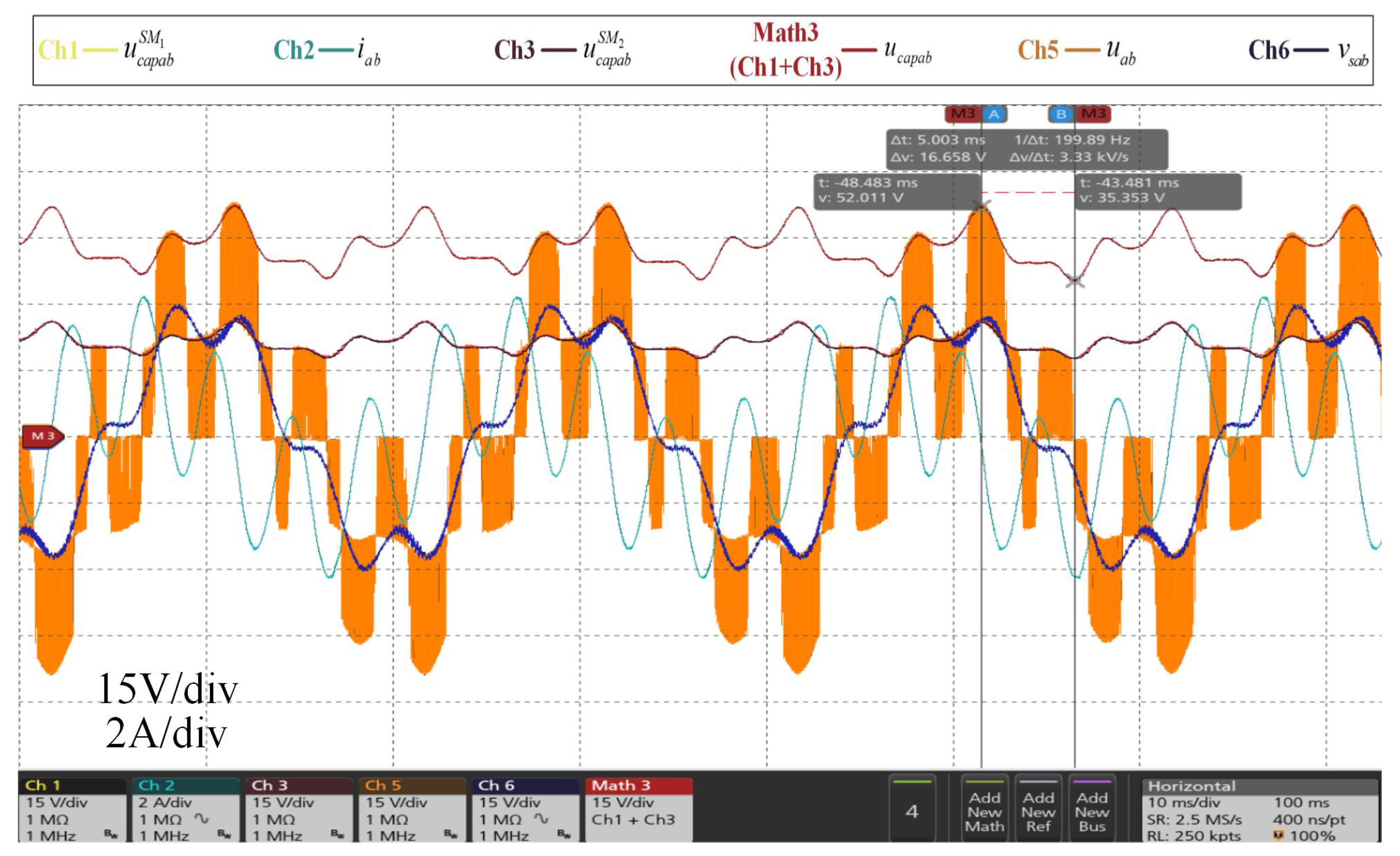
A down-scaled prototype for single-phase CHB, as in Figure 8, is built for experimental verification. In the experiment, the voltages and currents are and of those in the simulations, resulting in an experimental capacitance of 10 times the simulations. The branch inductor L = 4 mH. Each branch consists of 2 H-bridge submodules. As shown in Figure 9, the controller is implemented by FPGA and DSP. The capacitor voltages and branch currents are measured with sensors LV25-P and LAH-25P, the measured voltages/currents are then sent to FPGA and DSP using analog-to-digital chip. FPGA sends the switching signals to IGBTs via optical fibers. The online diagram of the whole system is shown in Figure 9. The experiments with , and are given, see Figure 10, Figure 11 and Figure 12. Moreover, the experimental results are summarized in Table 2.
In Figure 10, the current contains the 1st and 5th harmonics. The capacitor voltage contains multiple harmonics. The maximum and minimum value of are approximately 50.1 V and 37.3 V. All constraints are satisfied. The experimental result agrees with the simulation very well, validating the proposed sizing method. More detailed information about the positive and negative values of the capacitors voltages are listed in Table 2.
In order to validate the proposed strategy further, we evaluate the experiment results when µF and µF, see Figure 11 and Figure 12, respectively. When µF [see Figure 11], only , and are satisfied. is larger than the boundary value . For = 200 µF [see Figure 12], the peak voltage limitation is satisfied and the peak-peak voltage requirement is not satisfied, see Table 2.
6. Discussion
Most of the previous work about the CHB sizing is for reactive power compensation, where the branch voltage/current contains only the fundamental frequency component. The capacitance sizing for the delta-connected CHB-based active power filter is rarely studied. Nevertheless, there are some pieces of work for the capacitance sizing of an active power filter based on other power converter topologies. Here, the calculation for the capacitance value in [25] is compared with the proposed calculation, indicating the high accuracy of the proposed method. Using our introduced symbols, the expression of dc-link capacitance value, as presented in [25], is described as
where T is the fundamental frequency period, and is the amplitude of the branch current. Based on the the data from the simulations in Section 4, T = 0.02 s and A, which can be put into the above equation, the minimal capacitance in [25] can be obtained:
From the above analysis, the capacitance value should be , while in the proposed calculation, the capacitance value is [see Table 1]. The comparison of and indicates that the proposed method can result in a much lower capacitance value. Furthermore, this low capacitance can not only guarantee the power quality but also the safety performance. Because of the systematic nature of the proposed method, it can be easily generalized to capacitance sizing for other APF systems or CHB-based APF that needs to compensate for higher harmonic orders.
7. Conclusions
This paper has proposed the minimization of capacitance for delta-connected CHB-based APF, satisfying the constraints for power quality and system safety. As opposed to aluminum electrolytic capacitors, film capacitors have additional safety requirement for the peak–peak permissible voltage. This article takes the design rules concerning power quality and safety for film capacitors into consideration. Using the trigonometric function, the constraints are transformed into positive polynomials. The optimal problem with the minimum capacitance value as the objective function is subject to constraints. Using the optimal solver SeDuMi, an optimal capacitance value can be obtained. The simulations and experiments for reactive power and harmonic compensation under harmonic grid conditions validate that the obtained capacitance satisfies all the constraints.
It is well known that the capacitance value influences the converter cost and volume; therefore, the method is beneficial to a low-cost low-volume APF design if the allowable minimum capacitance is selected. The presented method can also be used in other power-electronic-based systems, especially for the applications where the low-frequency capacitor voltage harmonics should be an important consideration.
Author Contributions
Conceptualization, H.W.; methodology, H.W.; validation, H.W.; writing—original draft preparation, H.W.; writing—review and editing, H.W. and F.G.; project administration, H.W.; funding acquisition, H.W. All authors have read and agreed to the published version of the manuscript.
Funding
This work was supported by the Key Laboratory of Control of Power Transmission and Conversion (SJTU), Ministry of Education under Grant 2021AC02 and grants from the Delta Power Electronics Science and Education Development Program of the Delta Group.
Data Availability Statement
The data can be provided if required.
Conflicts of Interest
The authors declare no conflict of interest.
References
- Rao, B.N.; Suresh, Y.; Panda, A.K.; Naik, B.S.; Jammala, V. Development of cascaded multilevel inverter based active power filter with reduced transformers. CPSS Trans. Power Electron. Appl. 2020, 5, 147–157. [Google Scholar] [CrossRef]
- Tarisciotti, L.; Formentini, A.; Gaeta, A.; Degano, M.; Zanchetta, P.; Rabbeni, R.; Pucci, M. Model Predictive Control for Shunt Active Filters With Fixed Switching Frequency. IEEE Trans. Ind. Appl. 2017, 53, 296–304. [Google Scholar] [CrossRef]
- Li, S.; Qi, W.; Tan, S.C.; Hui, S.Y. Integration of an Active Filter and a Single-Phase AC/DC Converter with Reduced Capacitance Requirement and Component Count. IEEE Trans. Power Electron. 2018, 31, 4121–4137. [Google Scholar] [CrossRef]
- Wang, H.; Blaabjerg, F. Reliability of Capacitors for DC-Link Applications in Power Electronic Converters—An Overview. IEEE Trans. Ind. Appl. 2014, 50, 3569–3578. [Google Scholar] [CrossRef]
- Angulo, M.; Ruiz-Caballero, D.A.; Lago, J.; Heldwein, M.L.; Mussa, S.A. Active Power Filter Control Strategy With Implicit Closed-Loop Current Control and Resonant Controller. IEEE Trans. Ind. Electron. 2013, 60, 2721–2730. [Google Scholar] [CrossRef]
- Mannen, T.; Fujita, H. Dynamic Control and Analysis of DC-Capacitor Voltage Fluctuations in Three-Phase Active Power Filters. IEEE Trans. Power Electron. 2016, 31, 6710–6718. [Google Scholar] [CrossRef]
- Bai, H.; Wang, X.; Blaabjerg, F. A Grid-Voltage-Sensorless Resistive-Active Power Filter With Series LC-Filter. IEEE Trans. Power Electron. 2018, 33, 4429–4440. [Google Scholar] [CrossRef]
- Kong, Z.; Huang, X.; Wang, Z.; Xiong, J.; Zhang, K. Active Power Decoupling for Submodules of a Modular Multilevel Converter. IEEE Trans. Power Electron. 2018, 33, 125–136. [Google Scholar] [CrossRef]
- Mellincovsky, M.; Yuhimenko, V.; Zhong, Q.C.; Mordechai Peretz, M.; Kuperman, A. Active DC Link Capacitance Reduction in Grid-Connected Power Conversion Systems by Direct Voltage Regulation. IEEE Access 2018, 6, 18163–18173. [Google Scholar] [CrossRef]
- Du, X.; Zhou, L.; Lu, H.; Tai, H.M. DC Link Active Power Filter for Three-Phase Diode Rectifier. IEEE Trans. Ind. Electron. 2012, 59, 1430–1442. [Google Scholar] [CrossRef]
- Bhus, V.; Lin, J.; Weiss, G. The modular active capacitor for high power ripple attenuation. CPSS Trans. Power Electron. Appl. 2021, 6, 251–262. [Google Scholar] [CrossRef]
- Jia, G.; Chen, M.; Tang, S.; Zhang, C.; Zhu, G. Active Power Decoupling for a Modified Modular Multilevel Converter to Decrease Submodule Capacitor Voltage Ripples and Power Losses. IEEE Trans. Power Electron. 2018, 36, 2835–2851. [Google Scholar] [CrossRef]
- Jin, C.; Tang, Y.; Wang, P.; Liu, X.; Zhu, D.; Frede. Reduction of dc-link capacitance for three-phase three-wire shunt active power filters. In Proceedings of the IECON 2013—39th Annual Conference of the IEEE Industrial Electronics Society, Vienna, Austria, 10–13 November 2013. [Google Scholar]
- Isobe, T.; Shiojima, D.; Kato, K.; Hernandez, Y.R.R.; Shimada, R. Full-Bridge Reactive Power Compensator With Minimized-Equipped Capacitor and Its Application to Static Var Compensator. IEEE Trans. Power Electron. 2016, 31, 224–234. [Google Scholar] [CrossRef]
- Liu, Z.; Li, K.J.; Wang, J.; Javid, Z.; Wang, M.; Sun, K. Research on Capacitance Selection for Modular Multi-Level Converter. IEEE Trans. Power Electron. 2019, 34, 8417–8434. [Google Scholar] [CrossRef]
- Aluminum Electrolytic Capacitors—General Technical Information; Technical Report, TDK Electronics AG. 2022. Available online: https://www.tdk-electronics.tdk.com/download/185386/e724fb43668a157bc547c65b0cff75f8/pdf-generaltechnicalinformation.pdf (accessed on 1 August 2022).
- Farivar, G.; Hredzak, B.; Agelidis, V.G. Reduced-Capacitance Thin-Film H-Bridge Multilevel STATCOM Control Utilizing an Analytic Filtering Scheme. IEEE Trans. Ind. Electron. 2015, 62, 6457–6468. [Google Scholar] [CrossRef]
- Oliveira, R.; Yazdani, A. An Enhanced Steady-State Model and Capacitor Sizing Method for Modular Multilevel Converters for HVdc Applications. IEEE Trans. Power Electron. 2018, 33, 4756–4771. [Google Scholar] [CrossRef]
- Marcos-Pastor, A.; Vidal-Idiarte, E.; Cid-Pastor, A.; Martínez-Salamero, L. Minimum DC-Link Capacitance for Single-Phase Applications With Power Factor Correction. IEEE Trans. Ind. Electron. 2020, 67, 5204–5208. [Google Scholar] [CrossRef]
- Wang, H.; Wang, F.; Gao, F.; Cheng, J. Submodule Capacitor Sizing for Cascaded H-Bridge STATCOM with Sum of Squares Formulation. In Proceedings of the 2022 International Power Electronics Conference (IPEC-Himeji 2022—ECCE Asia), Himeji, Japan, 15–19 May 2022. [Google Scholar]
- Wang, H.; Liu, S. Harmonic Interaction Analysis of Delta-Connected Cascaded H-Bridge-Based Shunt Active Power Filter. IEEE J. Emerg. Sel. Top. Power Electron. 2020, 67, 5204–5208. [Google Scholar] [CrossRef]
- Film Capacitors—General Technical Information; Technical Report, EPCOS AG. 2018. Available online: https://www.vishay.com/docs/26033/gentechinfofilm.pdf (accessed on 24 March 2022).
- Labit, Y.; Peaucelle, D.; Henrion, D. SEDUMI INTERFACE 1.02: A tool for solving LMI problems with SEDUMI. In Proceedings of the IEEE International Symposium on Computer Aided Control System Design, Hyderabad, India, 18–20 September 2002. [Google Scholar]
- Wang, H.; Liu, S. An optimal operation strategy for an active power filter using cascaded H-bridges in delta-connection. Electr. Power Syst. Res. 2019, 175, 105918. [Google Scholar] [CrossRef]
- Gulez, K.; Adam, A.A.; Pastaci, H. Torque Ripple and EMI Noise Minimization in PMSM Using Active Filter Topology and Field-Oriented Control. IEEE Trans. Ind. Electron. 2008, 55, 251–257. [Google Scholar] [CrossRef]
Figure 1.
An active power filter with film capacitors applied at dc-link. (a) An APF connected in parallel with the loads. (b) Reduced Capacitance.
Figure 1.
An active power filter with film capacitors applied at dc-link. (a) An APF connected in parallel with the loads. (b) Reduced Capacitance.
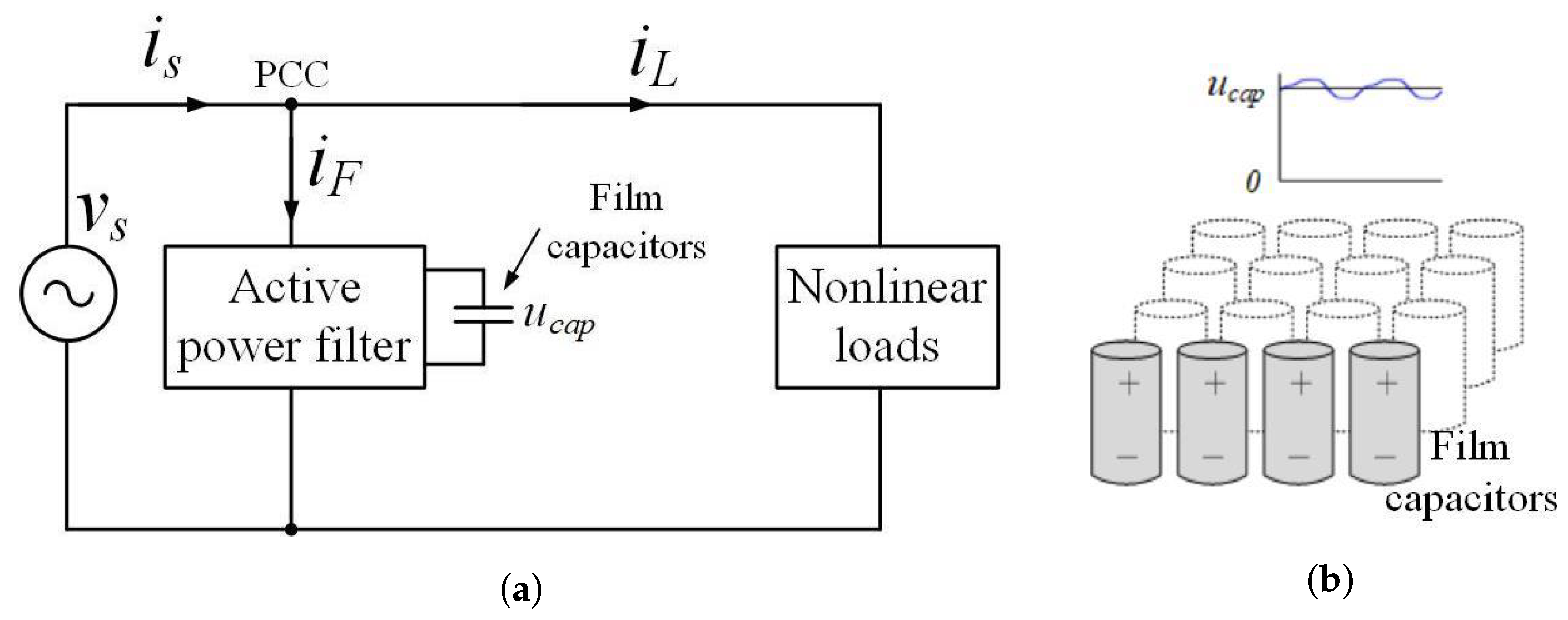
Figure 2.
Delta-connected CHB-based active power filter connected to the grid.

Figure 3.
Alternating voltage limit for film capacitors [22].
Figure 3.
Alternating voltage limit for film capacitors [22].
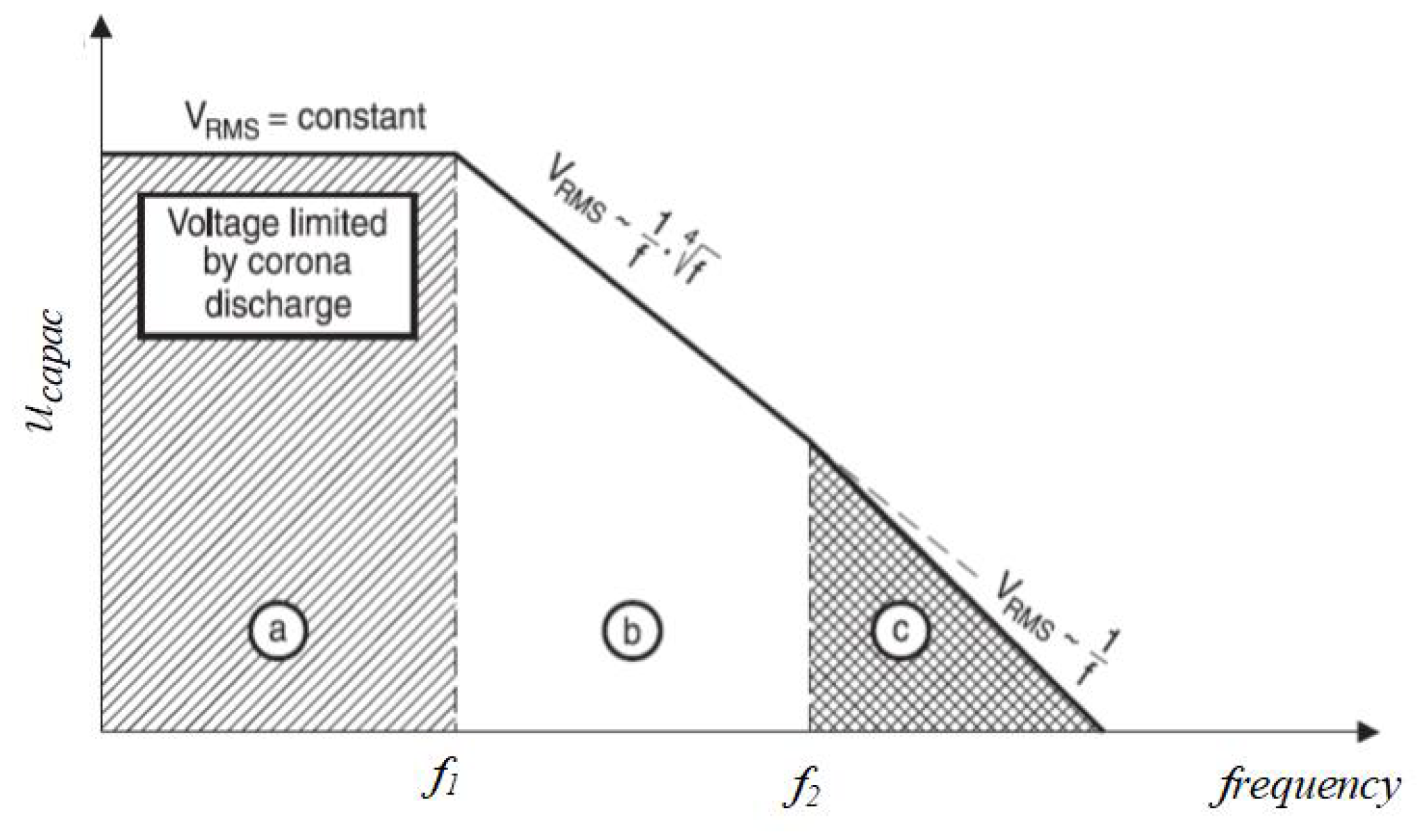
Figure 4.
Waveforms of the capacitor voltage and the absolute value of the branch voltage for harmonic compensation [the branch voltage containing the 1st and 5th as an example].
Figure 4.
Waveforms of the capacitor voltage and the absolute value of the branch voltage for harmonic compensation [the branch voltage containing the 1st and 5th as an example].
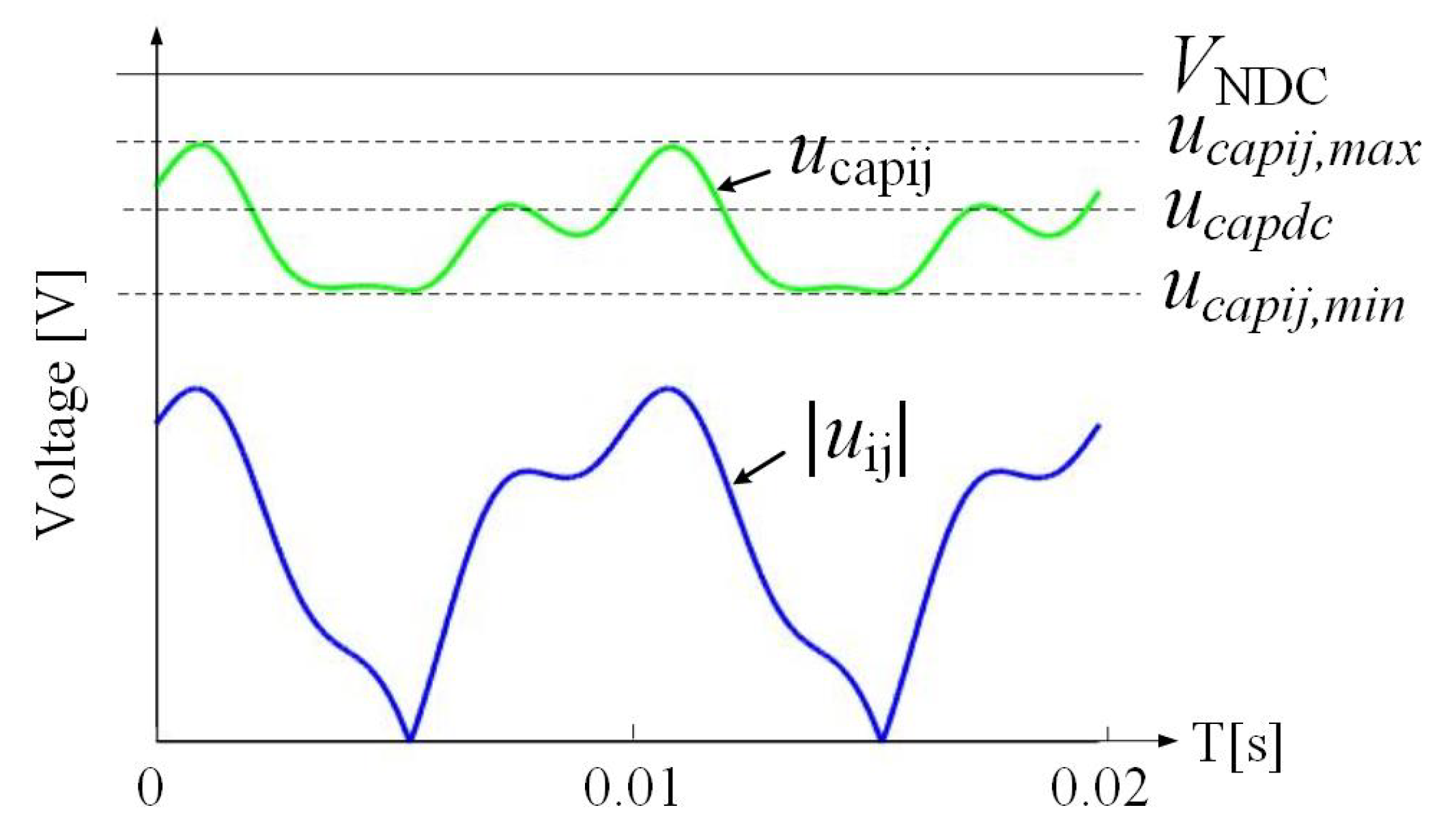
Figure 5.
Flow chart to calculate the optimal capacitance value.
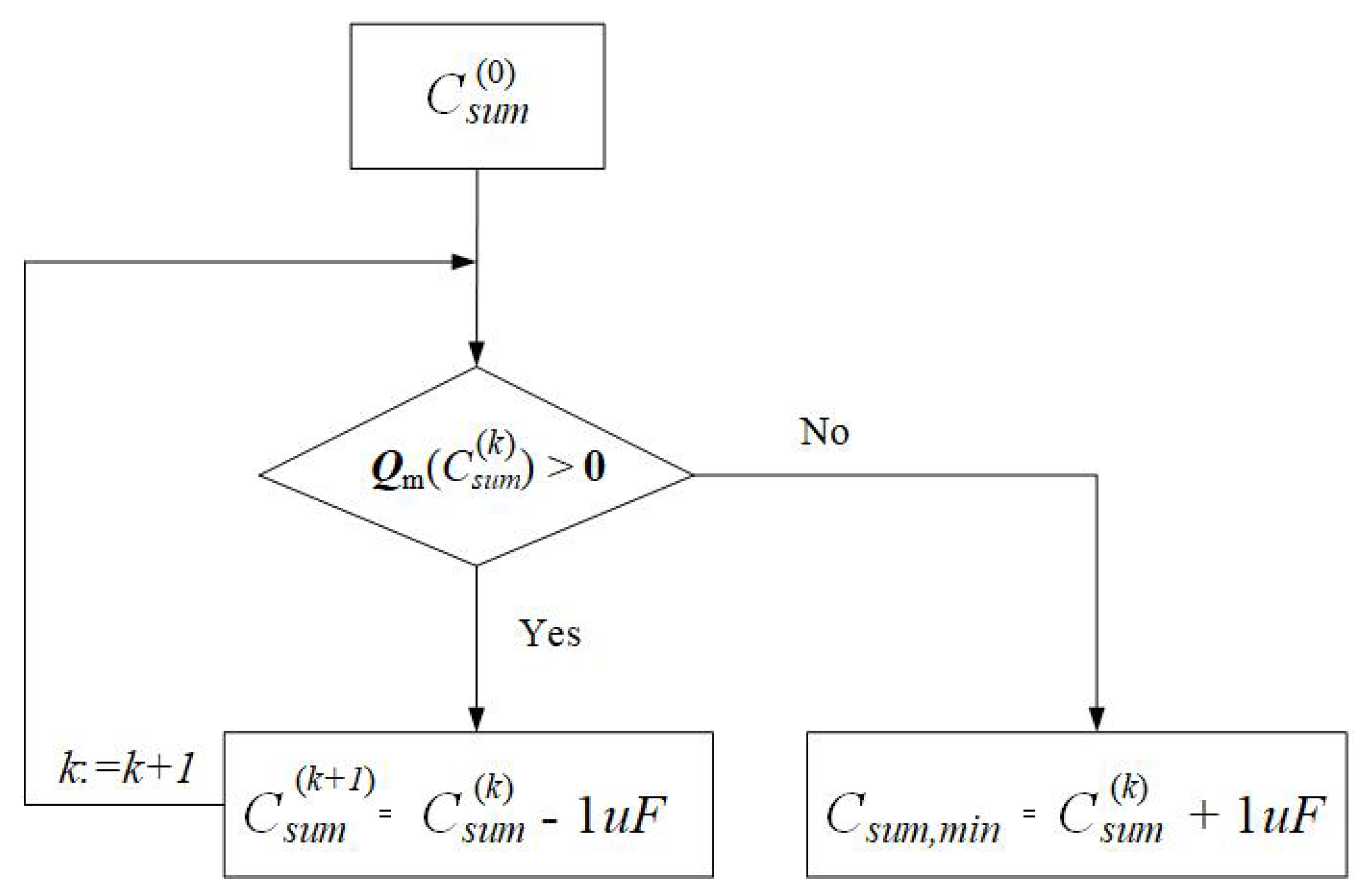
Figure 6.
Three-phase simulation results with (0.02 s–0.06 s), (0.06 s–0.1 s), (0.1 s–0.14 s), (0.14 s–0.18 s) and (0.18 s–0.22 s). The converter is injected at t = 0.02 s. From top to bottom are PCC line-line voltages, source currents, branch currents, the sum of SM capacitor voltages of each branch.

Figure 7.
The capacitor voltage and the absolute value of the branch- voltage with . (Left): time-domain waveforms. (Right): Spectra components.
Figure 7.
The capacitor voltage and the absolute value of the branch- voltage with . (Left): time-domain waveforms. (Right): Spectra components.
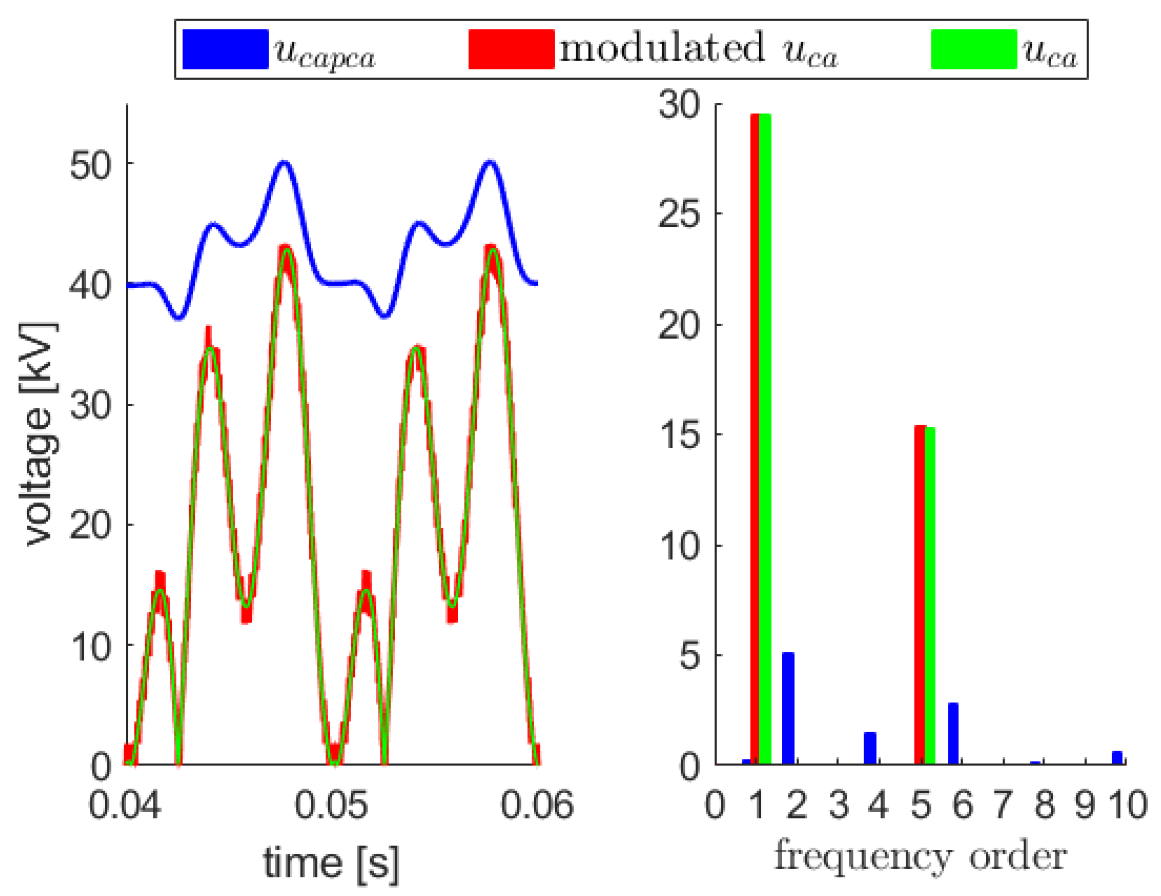
Figure 8.
A down-scaled prototype for single-phase CHB.
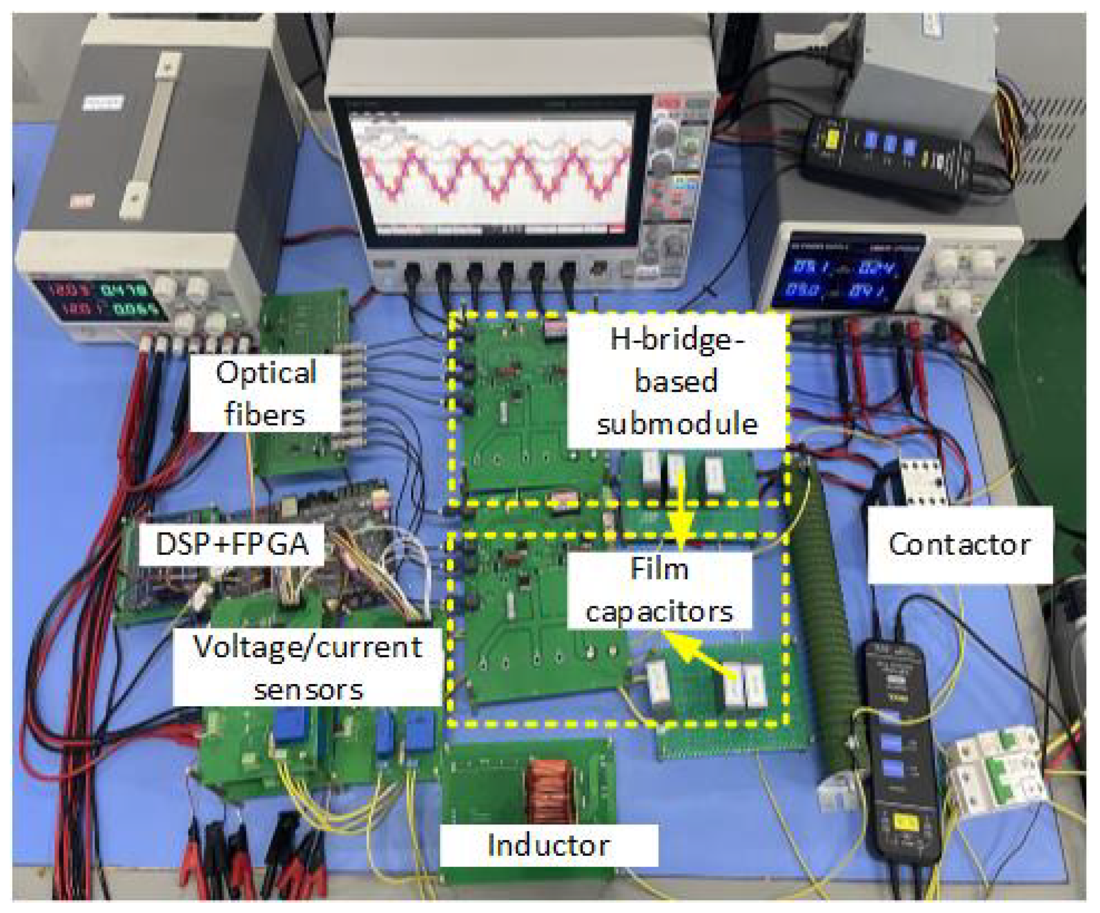
Figure 9.
Online Diagram for single-phase CHB.
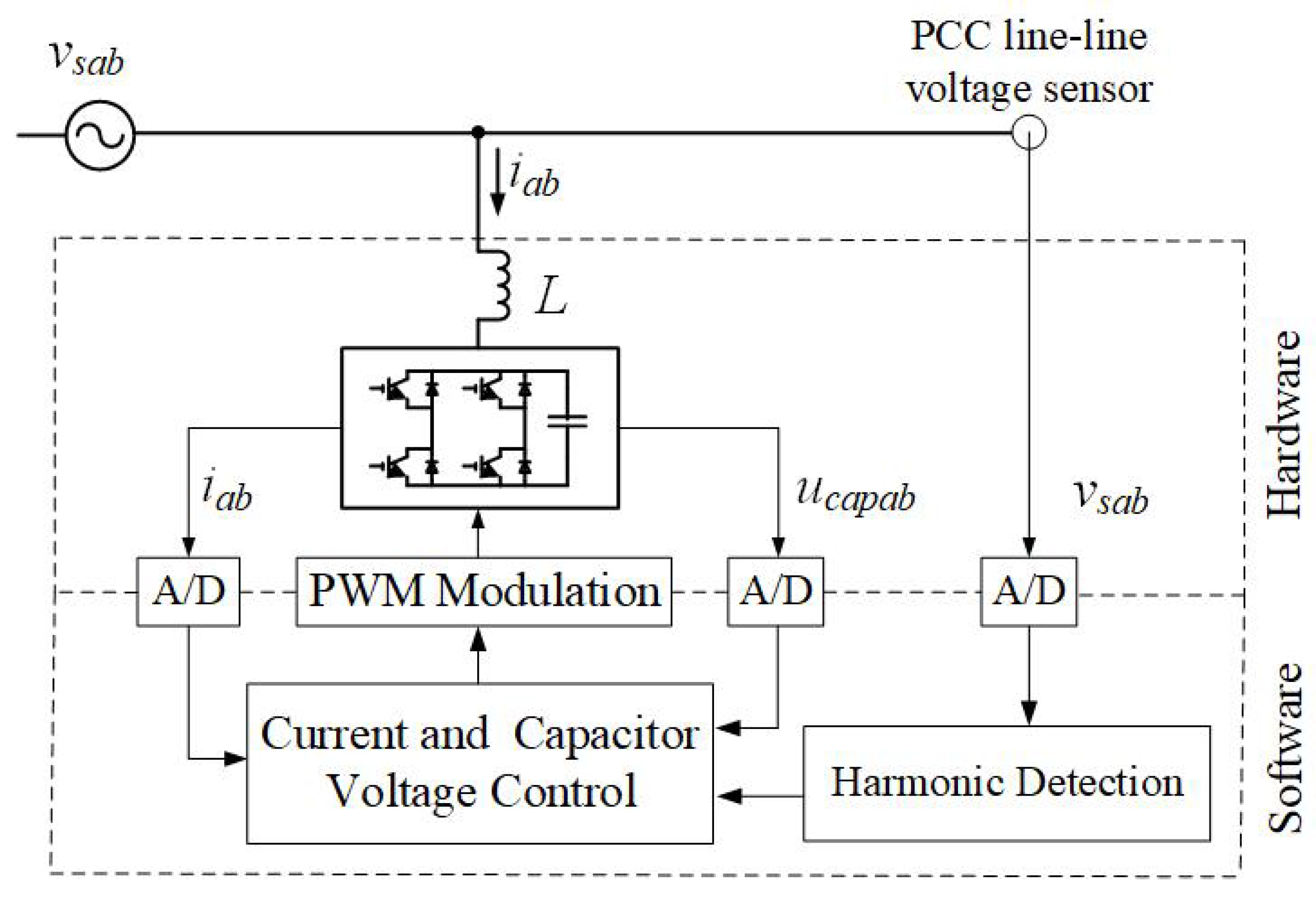
Figure 10.
Harmonic operation mode of CHB converter with µF.

Figure 11.
Harmonic operation mode of CHB converter with µF.
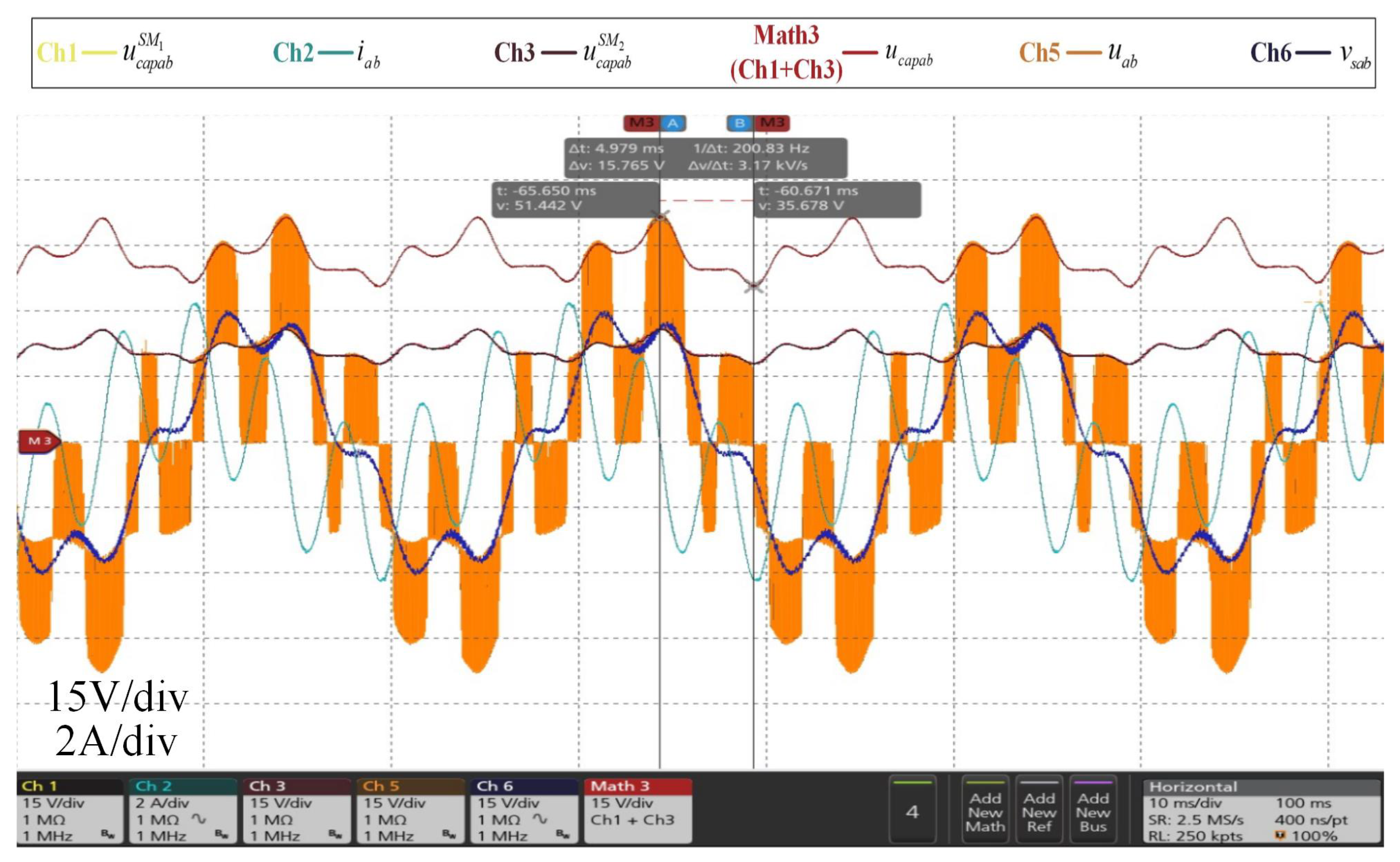
Figure 12.
Harmonic operation mode of CHB converter with µF.

Table 1.
Summary of the simulation results.
| Constraints (19), (25), (29), (30) | |||||
|---|---|---|---|---|---|
| µF | kV | kV | All constraints satisfied | ||
| µF | 51.7 kV | 35.9 kV | (19), (25),(30) satisfied, omitting (29) | ||
| µF | 50.1 kV | 37.3 kV | (19), (25),(29) satisfied, omitting (30) | ||
| µF | 52.2 kV | 35.5 kV | (19), (25) satisfied, omitting (29), (30) | ||
| µF | 66.7 kV | 17.7 kV | (19) satisfied, omitting (25), (29) and (30) |
Disclaimer/Publisher’s Note: The statements, opinions and data contained in all publications are solely those of the individual author(s) and contributor(s) and not of MDPI and/or the editor(s). MDPI and/or the editor(s) disclaim responsibility for any injury to people or property resulting from any ideas, methods, instructions or products referred to in the content. |
© 2023 by the authors. Licensee MDPI, Basel, Switzerland. This article is an open access article distributed under the terms and conditions of the Creative Commons Attribution (CC BY) license (https://creativecommons.org/licenses/by/4.0/).
Share and Cite
MDPI and ACS Style
Wang, H.; Gao, F. An Optimal Strategy for Submodule Capacitance Sizing of Cascaded H-Bridge-Based Active Power Filter. Electronics 2023, 12, 4444. https://doi.org/10.3390/electronics12214444
AMA Style
Wang H, Gao F. An Optimal Strategy for Submodule Capacitance Sizing of Cascaded H-Bridge-Based Active Power Filter. Electronics. 2023; 12(21):4444. https://doi.org/10.3390/electronics12214444
Chicago/Turabian StyleWang, Hengyi, and Fei Gao. 2023. "An Optimal Strategy for Submodule Capacitance Sizing of Cascaded H-Bridge-Based Active Power Filter" Electronics 12, no. 21: 4444. https://doi.org/10.3390/electronics12214444
Note that from the first issue of 2016, this journal uses article numbers instead of page numbers. See further details here.