
Basic Mechanisms of Single-Event Occurrence in Silicon Carbide Semiconductor under Terrestrial Atmospheric Neutron Irradiation

1
Aix-Marseille Univ, CNRS, IM2NP (UMR 7334), 13397 Marseille CEDEX 20, France
2
Univ. Rennes, CNRS, IPR (UMR 6251), 35 042 Rennes CEDEX, France
*
Author to whom correspondence should be addressed.
Electronics 2023, 12(21), 4468; https://doi.org/10.3390/electronics12214468
Submission received: 7 October 2023
/
Revised: 21 October 2023
/
Accepted: 28 October 2023
/
Published: 30 October 2023
(This article belongs to the Special Issue Radiation Tolerant Electronics, Volume III)
Abstract
:This numerical simulation work investigates the basic physical mechanisms of single events induced in a target layer composed of silicon carbide exposed to natural radiation with atmospheric neutrons at the terrestrial level. Using direct calculations and extensive Geant4 simulations, this study provides an accurate investigation in terms of nuclear processes, recoil products, secondary ion production and fragment energy distributions. In addition, the thorough analysis includes a comparison between the responses to neutron irradiation of silicon carbide, carbon (diamond) and silicon targets. Finally, the consequences of these interactions in terms of the generation of electron–hole pairs, which is a fundamental mechanism underlying single-event transient effects at the device or circuit level, are discussed in detail.
1. Introduction
Silicon carbide (SiC) is a wide-bandgap semiconductor material that offers numerous advantages and exceptional performance characteristics, which make it ideal for various applications [1,2,3,4,5,6,7,8]. Silicon carbide has excellent thermal conductivity and can withstand extremely high temperatures, even exceeding 600 degrees Celsius. Unlike silicon (Si) devices, SiC remains resilient, making it a game changer in industries with extreme heat requirements, such as the aerospace and energy industries [4]. In addition, SiC’s tolerance for high temperatures allows for more compact and lightweight systems, critical in space- and weight-constrained applications. For these properties, silicon carbide is used for applications in high-temperature environments such as power electronics and automotive industries [9,10,11]. Another outstanding feature of SiC devices is their ability to withstand much higher breakdown voltages than their Si counterparts [11]. This feature makes them indispensable in applications requiring robust voltage tolerance, like high-voltage power transmission and electric vehicle management [4,12]. Since it exhibits high breakdown voltage and low power losses, SiC is extensively employed in power electronics [12,13,14], such as inverters and converters. In addition, the fast-switching speed of silicon carbide and its high-frequency capabilities [14,15] make it suitable for RF systems, wireless communication and radar applications. Furthermore, SiC’s compatibility with Si processing techniques facilitates its integration into existing semiconductor manufacturing processes.
From the point of view of resistance to radiation, a large number of studies published in the literature have shown that silicon carbide exhibits excellent radiation hardness, withstanding high levels of radiation without significant degradation. It maintains its mechanical and thermal stability under irradiation, ensuring its effectiveness in nuclear reactors and space environments [4,16,17,18,19]. Most of the research conducted in this field concerns the response to radiation of devices and circuits made from SiC, especially power devices [9,10,20,21,22,23,24,25,26,27]. Few works have been carried out to examine the effects of neutron radiation at the material level on bulk SiC (i.e., not integrated into electronic devices). For example, some previous studies [28,29] have investigated the vulnerability of several materials from group IV or compound III–V materials, including SiC. However, these results are limited in terms of (i) energy of secondary charged particles (also called secondary products) issued from atmospheric neutron interactions with the material (due to a limiting energy threshold, considered in [28]), (ii) event statistics [28], because a relatively low number of incident neutrons impacts the simulation results, and (iii) energy of incident neutrons, since the study in [29] concerns only monoenergetic incident neutrons (deuterium–deuterium or deuterium–tritium fusion neutrons). In the present work, we extensively explore the fundamental physical mechanism of single-event generation within a target layer composed of SiC induced by high-energy (>1 MeV) atmospheric neutrons at sea level. In contrast to previous works, this study was conducted without any restrictions on the energy of secondary products, covering a wide energy range and a significant number of incident neutrons. We examine the initial stages of atmospheric neutron-induced single-event effects (SEE) production in the target material. These single-event effects occur due to interactions between neutrons generated in atmospheric cascading showers and a bulk material target exposed to the natural neutron flux at ground level. Neutron interactions lead to the generation of secondary charged particles, which deposit their energy in the material and create electron–hole pairs along their trajectory [30]. The main objective of this work is to accurately quantify the intrinsic response of silicon carbide bulk material to neutron radiation, free from any external influences introduced by devices or circuits. However, in the forthcoming discussion, we will show that quantitative data obtained from these initial steps at the material level can provide valuable insights into the radiation susceptibility of electronic devices based on silicon carbide when exposed to atmospheric neutron flux at ground level. Since silicon carbide can be considered a mixture of carbon and silicon, we also considered carbon and silicon targets submitted to the same neutron irradiation as the silicon carbide target. Then, a meticulous and systematic comparison was conducted between the response of silicon carbide to neutron irradiation and the response of carbon and silicon targets. We used the Geant4 toolkit [31,32,33,34] to create a specific source of atmospheric neutrons and to compile extensive databases comprising the interaction events between neutrons and semiconductor target materials resulting from tens of thousands of interactions and representing 2.5 × 10⁷ h of irradiation in the natural background at sea level. The paper is organized as follows: in Section 2, we present the properties of the materials investigated here, the numerical atmospheric neutron source used in the simulation, along with details concerning direct calculations of the number of events and more sophisticated Monte Carlo numerical simulation of neutron–target interactions. Section 3 reports the extensive results of these simulations regarding the number of interactions, the number and nature of secondary products as well as their energy, linear energy transfer (LET) and range, the deposited energy, the generation of electron–hole pairs and the subsequent deposited charge. In Section 4, we thoroughly discuss all these results, particularly concerning the neutron susceptibility of SiC-based CMOS devices and circuits. This section also includes a comparative evaluation of their radiation resistance when compared to more conventional silicon-based devices.
2. Materials and Methods
2.1. Materials Properties
In this study, we consider semiconductor materials with isotopic compositions mimicking the natural abundance of nuclides. Table 1 provides a summary of the isotopes and their natural abundance for carbon and silicon, while Table 2 shows several characteristics, such as density, number of atoms per cm3, energy bandgap and energy value for electron–hole pair creation in bulk materials, of the semiconductors under study. Silicon has three isotopes, whereas carbon has two isotopes. However, it is reasonable to consider natural carbon as consisting entirely of the 12C isotope, since the minor isotope of carbon is a negligible fraction (about one percent). Both carbon and silicon carbide materials exhibit a higher density compared to silicon (2.329 g/cm3) owing to their atomic composition and crystallographic structure. Furthermore, they have a much larger number of atoms per cubic centimeter than silicon. This issue can directly impact the frequency of neutron interactions per unit volume of the material, as will be discussed in the following. In addition, both carbon and silicon carbide have a larger energy bandgap compared to silicon, resulting in higher energy required for electron–hole pair creation (3.6 eV for silicon) [35]. The electrical implications of this key parameter will be addressed in Section 4.
2.2. Atmospheric Neutron Source
To begin, it is important to recall that the Earth’s upper atmosphere experiences interactions between primary cosmic rays and atmospheric particles, leading to the formation of atmospheric showers that generate secondary particles that reach sea level [36]. Neutrons are the second most prevalent type of particle at sea level, after muons. Among these secondary particles, high-energy neutrons (usually above 1 MeV) constitute by far the most significant risk to ground-level electronics. This is primarily because these particles are not charged, making them highly intrusive and capable of deeply penetrating circuit materials. Within these materials, they can interact with atoms, producing charged products such as recoil nuclei or secondary ions, as explained below.
In order to simulate the atmospheric neutron source, the differential flux of high-energy neutrons induced by cosmic rays, as measured by Goldhagen in Yorktown Heights [37] and shown in Figure 1, has been adopted as the reference input spectrum in this work for the calculation of neutron interactions with the materials under investigation. This differential flux was previously modeled by Gordon et al. [38] using an analytical fitting function given by:
with A = 1.006 × 10⁻⁶, B = −0.35, C = 2.1451, D = 1.011 × 10⁻³, F = −0.4106 and G = −0.667. This model will be used in the following for the atmospheric spectrum.
2.3. Classification of Neutron Interactions
Neutron interactions with atomic nuclei can be classified into two primary mechanisms: scattering and capture. Scattering can be further divided into two types: elastic and inelastic scattering [36,39]. Elastic scattering occurs when the interacting particles remain unchanged, resulting in the recoil nucleus being the same as the target nucleus (Si or C in this case). Inelastic scattering is similar to elastic scattering, except that the target nucleus undergoes an internal rearrangement, leading to an excited state and eventual radiation release. In addition to scattering, an incident neutron can also be absorbed or captured by the nucleus of the target material. Such interactions give rise to a range of possible reactions and the emission of various particles. These interactions are commonly referred to as nonelastic interactions.
2.4. Direct Calculation of the Number of Interactions
To rapidly evaluate the vulnerability of the materials under investigation to atmospheric neutrons, one can make a rough assessment by directly calculating the reaction rate in a target that represents a microelectronic circuit [35]. This calculation can be accomplished through analytical methods using data from a neutron cross-section library. In this work, we used the TENDL nuclear data library [40], which provides neutron cross-section information up to 200 MeV. Figure 2a,b illustrate the total, elastic and inelastic cross-sections for the predominant carbon and silicon isotopes, respectively.
The nuclear reaction rate (number of reactions per second), denoted as Rn, occurring in a material layer with an area of S = 1 cm2 and a thickness of ttarget = 20 µm, can be directly calculated by:
where N is the number of atoms per cm3 of the considered material (see Table 2), σ(E) is the neutron cross-section of the material, dφ/dE is the differential neutron flux (MeV−1·cm−2·s−1), Emin and Emax are the limits of the energy domain considered and ttarget is expressed in cm. In our case, Emin = 1 MeV and Emax = 200 MeV. The differential neutron flux is given by Equation (1).
The number of reactions for a given time duration is simply given by Rn multiplied by the duration in seconds. In this study, we considered a total fluence of 5 × 10⁸ atmospheric neutrons per cm2, which corresponds to an irradiation duration of 2.5 × 10⁷ h, equal to 9 × 10¹⁰ s.
2.5. Geant4 Simulation Details
Following this quick calculation of the number of interactions, a significantly more meticulous examination was conducted to acquire comprehensive insights into the mechanisms of neutron–material interactions. This analysis concerned not only the count of events but also explored in-depth aspects of the interaction process, such as discerning the nature of interactions (elastic, inelastic, nonelastic), determining the quantity and characteristics of reaction products, and investigating their energy distribution in detail. For this purpose, Monte Carlo simulations of the interactions between atmospheric neutrons and the materials under investigation were performed using Geant4 [31,32,33,34], following a methodology employed in previous studies [35,41,42]. Targets of pure bulk material, one for each material (silicon carbide, carbon, and silicon), were generated for the simulations. Every target has a parallelepiped geometry, with a surface area of 1 cm2 and a thickness of 20 μm. The dimensions of the target were carefully selected to mimic the typical dimensions of the sensitive volume within an integrated circuit. More specifically, a thickness of 20 µm was chosen, as any reaction product generating electrical charge beyond this depth would not drift or diffuse towards the active area (which refers to the sensitive region of the circuit located near the semiconductor surface). As a result, these reaction products would not contribute to the incidence of single events within the circuit [42].
In the simulation, we subjected every target to virtual neutron irradiation. The neutrons arrive perpendicularly to the surface and follow an energy distribution described by the atmospheric neutron spectrum at sea level, shown in Figure 1 and modeled by Equation (1). To accurately simulate the irradiation, and as previously indicated, we simulated the impact of 5 × 10⁸ neutrons which is equivalent to a cumulative irradiation time of 2.5 × 10⁷ h under the natural atmospheric neutron flux at sea level.
The simulations were performed using Geant4 version 4.9.4 patch 01. The physical processes used for these simulations are based on the standard package of physics lists, called QGSP_BIC_HP [33,34]. Further details concerning the simulations can be found in [28,35]. The outputs of each simulation include a series of files that contain exhaustive information regarding the interaction events between neutrons and the target material. This information contains, for every event, the type and coordinates of the interaction’s vertex, the energy of the incident neutron and a detailed list of all secondary particles generated during the interaction. Additionally, the energy and emission direction vectors for every emitted particle are recorded for each event.
In order to focus on particles with significant ionizing properties that have a noticeable impact on electronics in terms of electron-pair generation and single-events, we have deliberately excluded from the simulation particles with slight ionizing properties. As a result, the computed databases do not include electrons, positrons, gamma photons, neutral pions, neutrons or mesons. We have also excluded from the databases rare secondary particles, like charged pions. Instead, the resulting databases exclusively consist of protons, alpha particles and ionizing products with an atomic number (Z) greater than 2 (Z > 2).
3. Results
3.1. Number of Interactions
In Figure 3a, we present the simulation results, comparing the number of interactions obtained from the TENDL nuclear data library with those obtained through Monte Carlo simulations using Geant4. As mentioned above, for both types of simulation, we consider 5 × 10⁸ incident atmospheric neutrons and targets with a surface area of 1 cm2 and a thickness of 20 µm. The graph illustrates the total number of interactions, as well as the number of interactions attributed to specific mechanisms, namely elastic, inelastic and nonelastic interactions. For the calculations using TENDL, the number of nonelastic interactions is determined by subtracting the sum of elastic and inelastic interactions from the total number of interactions. Figure 3b shows the same results but in terms of the percentage of the total number of interactions for each type of mechanism. This allows for a relative comparison and understanding of the contribution of each interaction type to the overall number of interactions. The results indicate a very good agreement between the two calculation approaches, using TENDL and Geant4, for the three materials under study. The number of interactions is systematically slightly higher in Geant4 simulations compared to TENDL calculations, with an increase of approximately 3% for SiC and around 6% for C and Si. The reason for this difference is that the TENDL library is restricted to energies up to 200 MeV. However, the general trends remain consistent, and the percentage values associated with each mechanism type are very close (Figure 3b), with differences of less than 10%.
Figure 3a illustrates the disparity in the total number of interaction events among the three materials investigated in this study. Silicon exhibits the lowest interaction events (85,758 events in Geant4 simulations), whereas carbon presents a significantly higher count (195,839 events), more than double that of silicon, which results from an extremely high number of elastic events compared to silicon. Of the total number of carbon interactions, 80% are elastic interactions, while this percentage is 70% for silicon, as shown in Figure 3b. In particular, carbon experiences more than 2.5 times as many elastic interactions as silicon. This difference can be attributed to carbon’s exceptional neutron moderating capabilities, which consist of slowing down fast neutrons [43]. Carbon is an effective neutron moderator mainly because its low atomic mass and limited number of protons make it easier for fast neutrons to transfer kinetic energy to carbon atoms, thereby slowing them down.
When examining silicon carbide, which can be seen as a composite of silicon and carbon at the atomic level, as explained before, its behavior lies between that of silicon and carbon. Silicon carbide exhibits a total of 136,151 events, which represents a 58% increase in the number of reactions compared to silicon. However, a large majority of these events correspond to elastic reactions, accounting for approximately 75% of the overall reaction count for silicon carbide. Silicon carbide presents approximately 70% more elastic events compared to silicon, primarily attributed to the inclusion of carbon atoms within its structure. The large percentage of elastic reactions for silicon carbide can lead to less aggressive SEEs than for silicon, as explained later in the discussion.
3.2. Number and Nature of Secondary Products
Each interaction between an incoming neutron and the target material leads to the production of one or more secondary products. The number of secondary products resulting from a nuclear reaction is called “secondary product shower multiplicity” because each event can be seen as initiating a cascade of ionizing products. When the multiplicity is 1, indicating the emission of a single product, it corresponds to elastic or inelastic events. Higher multiplicities indicate the occurrence of nuclear reactions resulting in the production of two or more secondary products and correspond to nonelastic interactions. It is important to remember that, as explained in Section 2.4, products such as electrons, positrons, gamma photons, pions, neutrons and mesons are excluded from the databases and then from the multiplicity calculation. Figure 4 illustrates the number of events for each shower multiplicity and for the three target materials investigated in this work.
The data indicate a consistent trend across all three targets, where an increase in multiplicity results in a decrease in the number of reactions. Above certain values of multiplicity, specifically M = 7 for carbon, M = 14 for silicon and M = 15 for silicon carbide, the number of reactions becomes zero. The percentage of events for different values or ranges of multiplicity is detailed in Table 3.
The results show that reactions leading to a single product are by far the most numerous for all materials. In terms of multi-fragment reactions, those with a multiplicity of four or higher constitute a small yet noteworthy portion of the events for all semiconductors: 2.5% for C, 2.7% for SiC and almost 3% for Si. These high-multiplicity events hold significance as they can generate single events that potentially impact multiple sensitive areas within a component or circuit. Once the multiplicity exceeds 11, the statistical significance of the events reduces notably and possibly depends on the number of incident neutrons, as previously indicated in [28].
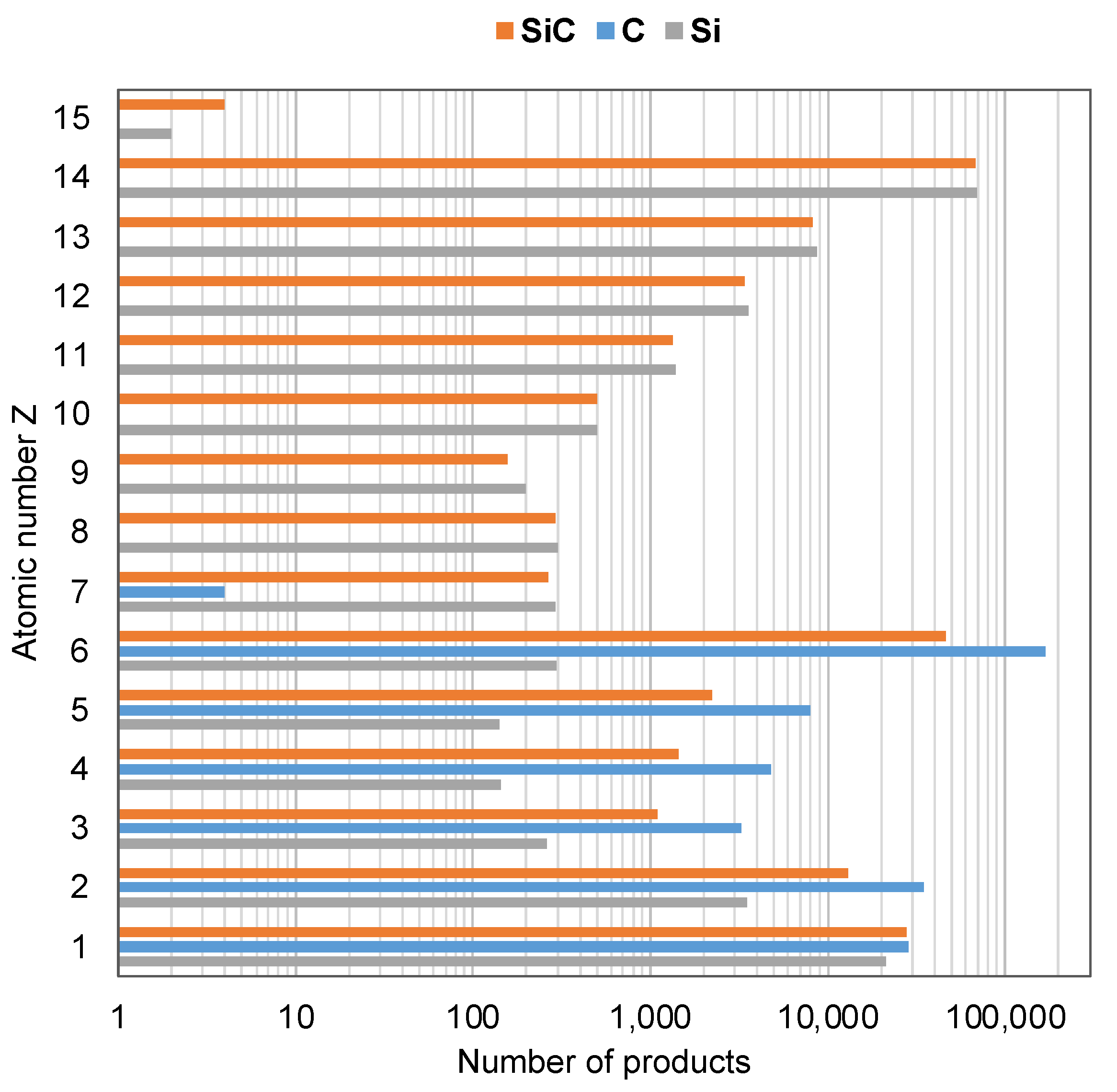
A comprehensive analysis of the generation of these secondary ions is presented in Figure 5, focusing on their dependence on the atomic number of the products. The range of atomic numbers (Z) considered spans from 1 (proton) to the highest atomic number found in the target material (here 6 for carbon and 14 for silicon and SiC), as is generally the case in neutron–matter interactions [44]. However, rare transmutation reactions can lead to products with larger atomic numbers (for example, 30Si is activated during irradiation by the capture of a thermal neutron and is converted into stable 31P with a half-life of 2.6 h). Due to the very high number of incident neutrons (500 million) considered in our simulations, this case clearly appears in our results (Figure 5) for a few carbon nuclei transmuted in nitrogen and for Si transmuted in P.
For the three materials, the most frequently produced secondary particles are recoil products resulting from the elastic interactions between neutrons and the nuclei of the semiconductor lattice. In the case of silicon carbide, the recoil nuclei correspond to two distinct species, Si and C. Following closely in second place are protons for silicon carbide and silicon and alpha particles for carbon. The third most frequently produced particles are alpha particles for SiC and Si and protons for carbon. Comparatively, all other particle types are consistently generated in smaller quantities than these three categories of products. Then, in the rest of this analysis, we classified the produced particles into the following categories: recoil nuclei, protons, alpha particles and other products.
3.3. Energy, LET and Range of Secondary Products
Figure 6a shows a histogram of the energy of the secondaries produced in the interactions between neutrons and silicon carbide target. As explained previously, the secondary products were classified into five categories for SiC according to their atomic number: protons (Z = 1), alpha particles (Z = 2), carbon recoil nuclei (Z = 6), silicon recoil nuclei (Z = 14) and other products (with all the remaining atomic numbers Z). These curves show the energy range covered for each type of particle and the energy position of the maximum of the distributions. Figure 6b presents the energy mapping for secondary products in silicon carbide. In this diagram, every colored dot represents a distinct secondary product. The horizontal position of each dot corresponds to the energy of the incident neutron that led to its formation, while the vertical position represents the kinetic energy of the secondary product after it is released from the reaction. Since the maximum energy of the secondary products cannot exceed that of the incident primary neutron, it is evident that all points are logically located below the diagonal line y = x, as illustrated in this figure. For comparison, Figure 7 and Figure 8 present curves and diagrams like those of Figure 6a,b, illustrating neutron interactions with carbon and silicon targets, respectively. The energy histograms in Figure 6a, Figure 7a and Figure 8a show the same information as in Figure 6b, Figure 7b and Figure 8b, respectively, but in a more compact and quantitative form. The energy mappings of the products depicted in Figure 6b, Figure 7b and Figure 8b facilitate a visual comparison and highlight the similarities and differences between the three materials studied in terms of vulnerability to atmospheric neutrons. Specifically, they provide insights into the distributions of protons, alphas, recoil nuclei and other products for the three target materials.
The results in Figure 6a show that, among these secondary products, protons have a broad distribution with a maximum around 6 MeV and a large tail distribution of up to 2 GeV. A similar distribution is found for protons in carbon and silicon (Figure 7a and Figure 8a). For carbon, the distribution maximum is situated at 10 MeV and for silicon, is at 5 MeV. Protons clearly outnumber all other particles for secondary product energies from about 3 MeV for silicon carbide and silicon (20 MeV for carbon) up to 1 GeV. As can be seen in Figure 6b, Figure 7b and Figure 8b, there are fewer protons in the reaction products for SiC (15.97%) than for silicon (19.26%). This is due to the presence of carbon, for which the interaction with neutrons results in reaction products with a low proportion of protons (11.48%). This is a positive aspect for SiC-based circuits because, as will be shown below, protons travel a long distance through matter before undergoing significant interaction, either by nuclear interaction with the nucleus for high-energy protons or coulombic forces for low-energy protons.
Alpha particles exhibit a clear peak distribution, ranging from several tens of keV to several tens of MeV, and reaching its highest value around 6 MeV for the three materials. Beyond a product energy of 10 MeV, alpha particles and protons become the most numerous particles. In the secondary products, silicon carbide has a higher abundance of alpha particle content compared to silicon, with proportions of 7.43% for SiC and 3.16% for Si. This disparity can be attributed to the presence of carbon, for which alpha particles are more abundant (14% of the total number of secondary products).
The recoil products systematically have a distribution peaking at low energy (0.3 MeV for carbon and 0.2 MeV for silicon) and varying between 1 keV and 20 MeV for carbon and 1 keV and several MeV for silicon. The higher the atomic number Z, the lower the energy limit of the recoil nuclei distributions. Also, the heavier the recoil nuclei, the lower the energy of the distribution maximum. For neutron interactions with the silicon carbide target, the Si recoils arise in a proportion of 38.85% and the C recoils at 26.74%. Other products (with atomic numbers other than 1, 2, 6 and 14) show a less broad distribution than recoil nuclei, with a maximum range of close to a few MeV (2 MeV for silicon carbide and silicon and 5 MeV for carbon) to up to a few tens of MeV. In silicon carbide, the proportion of other products is 10.98%, which is lower compared to silicon (14.3%).
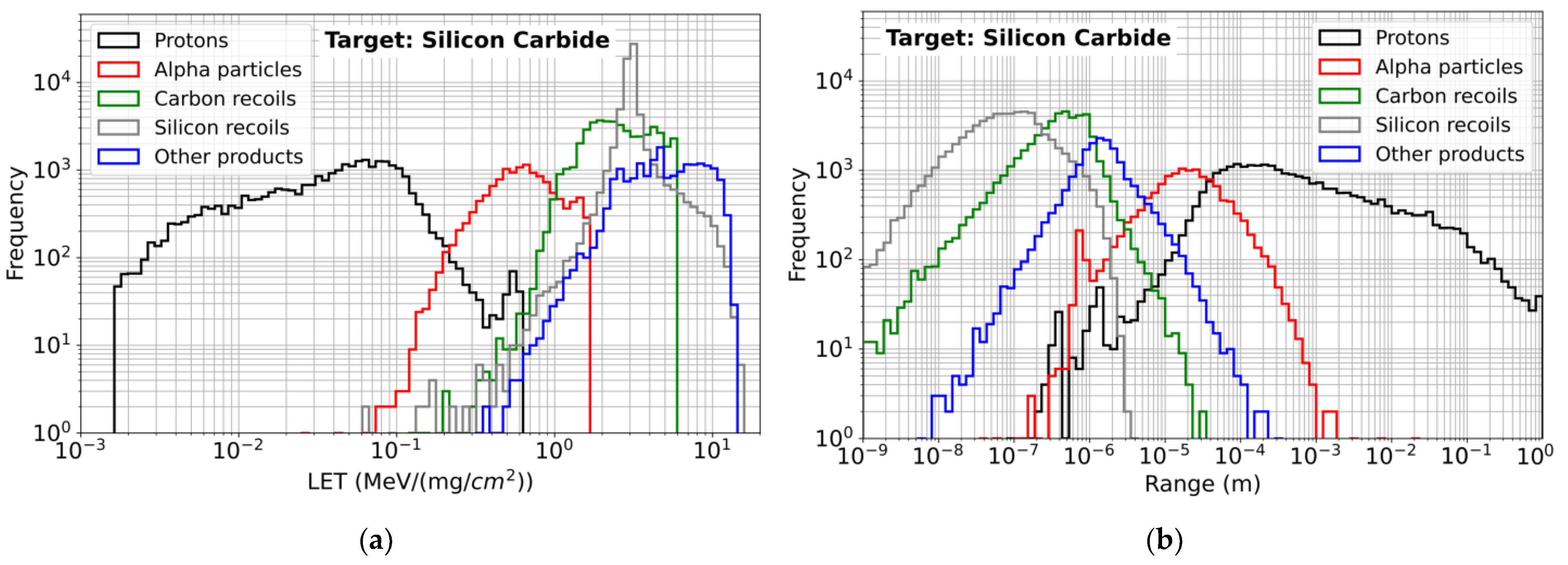
From the energy data for the secondary products of the neutron–SiC interactions presented above, we have deduced the LET and range distributions for all the secondary products. We remind the reader that the linear energy transfer (LET) of a charged particle refers to the electronic part of its stopping power, which denotes the energy dissipated per unit length as a result of electron collisions [36]. This quantity is typically expressed in units such as MeV/(mg/cm2) or keV/μm. The range is the distance covered by a charged particle from its emission point until it completely decelerates and stops in the matter. The LET and range values essentially depend on factors such as the particle type, the initial energy and the medium (i.e., the target material) through which the particle passes. To calculate the LET and range of secondary products in silicon carbide, we used the reference code SRIM (Stopping and Range of Ions in Matter) [45,46]. The particles considered are protons, alpha particles and carbon and silicon recoil nuclei. The LET and range curves as functions of the secondary product energy are illustrated in Figure 9 for silicon carbide, as well as for carbon and silicon, for easier comparison.
As expected, the variation in the LET with energy is the same for all particles. The LET initially increases as the particle energy increases until it reaches its maximum at the Bragg peak [36]. Beyond the Bragg peak, the LET decreases as the energy of the particle continues to increase. It should also be noted that secondaries with higher atomic numbers (Z), indicating higher charge, have higher stopping power and Bragg peaks. Concerning the range curves, we observe that the range increases continuously with the energy of the secondary product. As expected, for a given energy level, lighter particles exhibit longer ranges.
Figure 10, Figure 11 and Figure 12 present the histograms in LET and range for silicon carbide, carbon and silicon, respectively. The results indicate that protons, being the lightest yet most energetic particles, have the lowest LET values, ranging from a few 0.001 to a few 0.1 MeV/(mg/cm2). Additionally, high-energy protons can travel the longest distances, up to 1 m. These observations apply to the three materials under investigation. Alpha particles exhibit moderate LET values, with a peak distribution centered approximately at 6–8 MeV/(mg/cm2). Like protons, alpha particles are light particles and so are characterized by very long ranges. The most energetic alpha particles can reach distances of a few hundred microns in the case of silicon and up to 1 mm in the cases of silicon carbide and carbon. The LET values of the Si and C recoil nuclei are distributed according to a sharp distribution in all the targets, with a peak centered around 3 MeV/(mg/cm2) for silicon and 1 MeV/(mg/cm2) for carbon. The heavy secondary products composed of recoil nuclei (Si and C) and fragments other than protons and alpha particles exhibit the highest LET values, reaching up to about 10 MeV/(mg/cm2). Moreover, these recoil products (Si, C and other heavy products) have the shortest ranges, spanning from tens to hundreds of nanometers and up to a maximum of 300 microns.
3.4. Deposited Energy
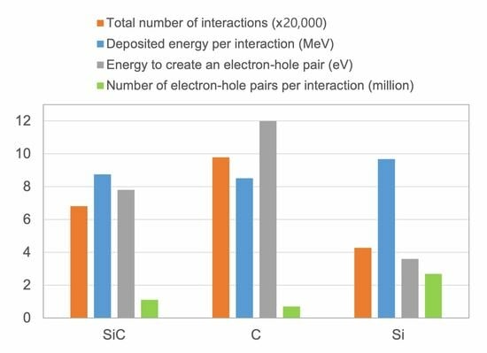
Results presented in previous sections were used to estimate the energy deposited in the semiconductor by neutrons interacting with SiC, C and Si targets. An average energy per interaction was calculated as the ratio between the total energy deposited by all products and the number of events. The results of these calculations, presented in Figure 13, indicate that the deposited energy is slightly reduced in silicon carbide compared to silicon (by approximately 9.5%) but is higher than in carbon. To provide a deeper analysis, we have conducted calculations to determine how different types of interactions contribute to the overall values. Our examination involved two types of interactions: (1) elastic or inelastic reactions, and (2) nonelastic reactions. It was found that elastic or inelastic reactions result in relatively small energy deposition for all materials (0.36 MeV for SiC). In contrast, nonelastic reactions deposit significantly higher energies, surpassing several tens of MeV (48.1 MeV for SiC). In the case of silicon carbide, the energy deposited in nonelastic reactions is more than 130 times greater than the energy deposited through elastic or inelastic events. However, as shown earlier, nonelastic reactions occur significantly less frequently compared to elastic or inelastic reactions. This disparity in occurrence accounts for the total average values remaining below 10 MeV for all materials.
In addition to the previous results, we have evaluated the proportion of total energy deposited by various types of secondary products in bulk semiconductors. Figure 14a presents the obtained values, which indicate that protons account for over 75% of the total energy deposition in all target materials, with percentages of 84% for SiC, 76% for carbon (C) and 90% for silicon (Si). Following protons, alpha particles occupy the second position, with 7.7% for SiC and 14% for C. Recoil nuclei and other products contribute separately to no more than 5% for SiC and C. Regarding silicon, other products represent approximately 5% of the energy deposition, while alphas only contribute 3%. Since protons and alphas exhibit large ranges, this result demonstrates that most of the energy is deposited far from the location of the point of interaction of the incident neutrons (also referred to as the reaction vertex). The fraction of the total initial LET deposited per type of secondary for all interaction events in the different materials can also be analyzed. The results of Figure 14b show that, for all materials, between 67.9% and 86% (minimum for Si, maximum for C) of the total initial LET values correspond to recoil nuclei. The other products represent 31% for Si, 22.8% for SiC and 9.8% for C. The contribution of protons and alpha particles, less than 5% for all materials, is negligible in this total initial LET. This implies that the charge deposited within the first few tens of nanometers around the reaction vertex is predominantly attributed to the recoil nuclei.
3.5. Generation of Electron–Hole Pairs and Deposited Charge
In order to determine the consequences of the results presented above on the operation of SiC-based CMOS devices and circuits subjected to neutron radiation, it is important to estimate the impact of neutron–SiC interactions on the creation of electron–hole pairs, which is a fundamental phenomenon underlying the occurrence of single-event effects. After being released following the neutron–matter interaction, the charged secondary products mainly interact with the electrons and nuclei of the target material [36]. The main mechanism that leads to energy loss and the slowing down of the charged particle is the ionization process. Ionization induces the generation of many excited energetic electrons (delta-rays), which generally have sufficient energy to ionize other atoms. These electrons produce a cascade of secondary electrons, which thermalize and create electron–hole pairs along the particle path. In a semiconductor, a large amount of the deposited energy is thus converted into electron–hole pairs. The energy necessary for the creation of an electron–hole pair, Eeh, depends on the material bandgap (values for SiC, C and Si are given in Table 2).
The number of electron pairs created per interaction is calculated as the ratio between the average deposited energy per interaction and Eeh for each material. Figure 15a shows that the number of electron–hole pairs is considerably lower in silicon carbide than in silicon, with about 58% fewer pairs being created in silicon carbide compared with silicon. This is mainly due to the higher energy required to create an electron–hole pair, 7.8 eV in silicon carbide versus 3.6 eV in silicon. This is a positive issue for silicon carbide from the point of view of single-event effects, as discussed in Section 4.
An additional noteworthy analysis involves the assessment of the charge Qdep deposited within the immediate vicinity of the reaction vertex points, specifically within the initial few nanometers. This value is calculated based on the initial LET of the particles immediately after their release, as described in reference [30]:
where tlayer is the thickness of the thin layer of material in which the charge Qdep is deposited, and K is a numerical factor that depends only on the density of the semiconductor material ρ and the value of Eeh (see Table 2) and is given by:
Using Equation (3), we estimate the charge deposited within the initial few nanometers surrounding the reaction vertex, considering all the secondary products across all interaction events in each material. The results for a distance of 10 nm are presented in Figure 15b, along with the current minimum critical charge requirement for standard SRAM memory cells in the 14 nm CMOS technology node [47]. For memory, the critical charge Qcrit is defined for memory circuits as the minimum amount of collected charge that will cause a device node to change its logical state and result in a single event upset [48]. The results demonstrate that silicon carbide exhibits a lower deposited charge Qdep compared to silicon, and the values for all three materials are below the critical charge threshold for the 14 nm CMOS technology node. The implications of these results will be discussed below.
4. Discussion
The results presented above allow us to discuss the impact of neutron interactions with silicon carbide on single-event effects and the radiation resistance of SiC-based CMOS devices and circuits, and to compare them with the reference silicon material. We begin by recalling the mechanisms underlying the effects of single events in devices following the creation of electron–hole pairs after neutron–matter interactions. The released carriers are rapidly transported and collected by reverse-biased junctions. Additionally, the deposited charges may recombine with other mobile carriers existing within the lattice. Charge transport relies on charge drift in electrically active areas and charge diffusion in neutral zones. The collected charges induce parasitic current transients, causing disturbances in the impacted device and in the related circuit, commonly referred to as single-event effects. These effects depend on the intensity of the current transient and the number of affected circuit nodes. High current levels can cause permanent damage like gate rupture or device latch-up. In low-power circuits, the transient current usually results in temporary changes in logical states, known as cell upsets. At this level, we can distinguish different cases: (i) a single-cell upset (SCU), where only one cell or logic element (latch, flip-flop, etc.) is upset [48]; (ii) a multiple-cell upset (MCU), which corresponds to a single event that induces several cells (e.g., memory cells or flip-flops) in an IC to flip their state at one time [48].
Returning to the present study on silicon carbide subjected to neutron irradiation, the number of interactions is found to be significantly higher compared to silicon. However, most of these interactions are elastic, resulting in a single reaction product, which is a recoil nucleus. Our results also indicate that recoil nuclei and other heavy products (excluding protons and alpha particles) have the potential to trigger single events within a short distance from where they are emitted, demonstrating a relatively high efficiency, but preferentially for SCUs. This is primarily attributed to their initial high LET values. Conversely, protons and alpha particles possess lower LET values but exhibit longer ranges in silicon carbide material. As a result, these particles can trigger single events at greater distances from their emission point and potentially induce a larger number of MCUs compared to heavy fragments. In consequence, single-event effects may be less severe in terms of MCUs when only a single reaction product is involved, in contrast to situations where multiple reaction products are generated, often including protons or alpha particles.
Another important observation pertains to the generation of electron–hole pairs in silicon carbide. The results indicate a considerable reduction in the number of electron–hole pairs created in silicon carbide compared to silicon. This disparity primarily arises from the higher energy required for the creation of an electron–hole pair in silicon carbide than in silicon. Then, the deposited charge available to be collected by collection structures will be comparatively lower for silicon carbide than for silicon. In addition, silicon carbide exhibits lower carrier mobility and shorter carrier lifetimes, with the latter factor leading to increased carrier recombination compared to silicon. Taking all these issues into account, current transients in SiC-based CMOS devices are expected to be weaker than those observed in silicon devices. Single-event effects may therefore be softer in SiC-based devices compared to Si devices. Nevertheless, it is important to note that a comprehensive and accurate analysis should also include the influence of the electric field on the collected charge and current transients and also consider carrier recombination mechanisms to effectively validate these observations. This would involve simulations conducted on given devices, which go beyond the scope of the current paper.
Finally, these remarks are supported by the earlier presented results on the charge deposition within the first 10 nm, which demonstrate that SiC exhibits a significantly lower deposited charge compared to Si. This implies that integrated electronics based on SiC are likely to experience reduced susceptibility to single-event effects caused by neutron exposure, in contrast to their silicon-based counterparts. Additionally, the observed charge level is below the critical charge threshold of SRAM memories in the 14 nm CMOS node. This observation suggests that SiC could potentially be integrated into CMOS technology down to the 14 nm scale. However, it is important to note that this prediction would need to be experimentally validated once silicon carbide-based CMOS devices and circuits are accessible for testing under neutron radiation conditions.
5. Conclusions
In this paper, we investigated the basic physical mechanisms of single-event generation in a target layer composed of SiC exposed to the natural radiation of high-energy atmospheric neutrons (>1 MeV) at the terrestrial level. This work was performed using direct calculations and Monte Carlo simulations with Geant4 to compile extensive databases of interaction events between neutrons and semiconductor materials resulting from tens of thousands of interactions. The simulation results showed that the silicon carbide undergoes significantly more interactions than a silicon target, but most of these interactions are elastic and result in only one reaction product. This product is a recoil nucleus that has the potential to trigger single events at a short distance from its emission point, preferentially a single-cell upset. This is different from multi-product reactions, which often include alpha particles and protons, because these light particles can trigger single events at greater distances from their point of emission and can potentially induce a greater number of multiple-cell upsets compared to heavy fragments. Since SiC undergoes more elastic interactions than Si (70% more elastic events in SiC than in Si), the effects of a single event may be less severe in terms of multiple-cell upsets because a single reaction product (heavy fragment) is more likely to be involved. Our results also indicate a significant reduction in the number of electron–hole pairs created in silicon carbide, with 58% fewer pairs compared to silicon. This difference is primarily due to the higher energy required to create an electron–hole pair in silicon carbide than in silicon. Considering the lower carrier mobility and stronger recombination in silicon carbide compared to silicon, the current transients induced by interactions with neutrons are expected to be weaker in silicon carbide than in silicon. This may be an indication of softer SEEs in SiC than in Si, although a more in-depth and accurate analysis is necessary, taking into account the influence of the electric field in a given device. Finally, the results show that SiC has significantly less charge deposited in the first 10 nm than Si. This suggests that SiC-based integrated electronics are likely to be less sensitive to the effects of single events caused by neutron exposure than their silicon-based counterparts.
Author Contributions
Conceptualization, D.M. and J.-L.A.; methodology, D.M. and J.-L.A.; software, D.M. and J.-L.A.; formal analysis, D.M. and J.-L.A.; investigation, D.M. and J.-L.A.; writing—review and editing, D.M. and J.-L.A.; visualization, D.M. and J.-L.A. All authors have read and agreed to the published version of the manuscript.
Funding
This research received no external funding.
Data Availability Statement
The data presented in this study are available on reasonable request from the corresponding authors.
Conflicts of Interest
The authors declare no conflict of interest.
References
- Dimitrijev, S.; Jamet, P. Advances in SiC power MOSFET technology. Microelectron. Reliab. 2003, 43, 225–233. [Google Scholar] [CrossRef]
- Hudgins, J.L.; Simin, G.S.; Santi, E.; Khan, M.A. An assessment of wide bandgap semiconductors for power devices. IEEE Trans. Power Electron. 2003, 18, 907–914. [Google Scholar] [CrossRef]
- Östling, M.; Ghandi, R.; Zetterling, C.M. SiC power devices—Present status, applications and future perspective. In Proceedings of the 23rd IEEE International Symposium on Power Semiconductor Devices and ICs, San Diego, CA, USA, 23–26 May 2011. [Google Scholar]
- La Via, F.; Alquier, D.; Giannazzo, F.; Kimoto, T.; Neudeck, P.; Ou, H.; Roncaglia, A.; Saddow, S.E.; Tudisco, S. Emerging SiC Applications beyond Power Electronic Devices. Micromachines 2023, 14, 1200. [Google Scholar] [CrossRef] [PubMed]
- Papanasam, E.; Prashanth Kumar, B.; Chanthini, B.; Manikandan, E.; Agarwal, L. A Comprehensive Review of Recent Progress, Prospect and Challenges of Silicon Carbide and its Applications. Silicon 2022, 14, 12887–12900. [Google Scholar]
- Ou, H.; Shi, X.; Lu, Y.; Kollmuss, M.; Steiner, J.; Tabouret, V.; Syväjärvi, M.; Wellmann, P.; Chaussende, D. Novel Photonic Applications of Silicon Carbide. Materials 2023, 16, 1014. [Google Scholar] [CrossRef] [PubMed]
- Coutinho, J.; Torres, V.J.B.; Capan, I.; Brodar, T.; Eres, Z.; Bernat, R.; Radulovic, V. Silicon carbide diodes for neutron detection. Nucl. Inst. Methods Phys. Res. A 2020, 986, 164793. [Google Scholar] [CrossRef]
- Bernat, R.; Capan, I.; Bakrac, L.; Brodar, T.; Makino, T.; Ohshima, T.; Pastuovic, Z.; Sarbutt, A. Response of 4h-SiC detectors to ionizing particles. Crystals 2021, 11, 10. [Google Scholar] [CrossRef]
- Shenai, K.; Galloway, K.F.; Schrimpf, R.D. The effects of space radiation exposure on power MOSFETs: A review. Int. J. High Speed Electron. Syst. 2004, 14, 445–463. [Google Scholar] [CrossRef]
- Galloway, K.F.; Witulski, A.F.; Schrimpf, R.D.; Sternberg, A.L.; Ball, D.R.; Javanainen, A.; Reed, R.A.; Sierawski, B.D.; Lauenstein, J.-M. Failure Estimates for SiC Power MOSFETs in Space Electronics. Aerospace 2018, 5, 67. [Google Scholar] [CrossRef]
- Pearton, S.J.; Aitkaliyeva, A.; Xian, M.; Ren, F.; Khachatrian, A.; Ildefonso, A.; Islam, Z.; Rasel, M.A.J.; Haque, A.; Polyakov, A.Y.; et al. Review—Radiation Damage in Wide and Ultra-Wide Bandgap Semiconductors. ECS J. Solid State Sci. Technol. 2021, 10, 055008. [Google Scholar] [CrossRef]
- Kumar, A.; Moradpour, M.; Losito, M.; Franke, W.-T.; Ramasamy, S.; Baccoli, R.; Gatto, G. Wide Band Gap Devices and Their Application in Power Electronics. Energies 2022, 15, 9172. [Google Scholar] [CrossRef]
- Prado, E.O.; Bolsi, P.C.; Sartori, H.C.; Pinheiro, J.R. An Overview about Si, Superjunction, SiC and GaN Power MOSFET Technologies in Power Electronics Applications. Energies 2022, 15, 5244. [Google Scholar] [CrossRef]
- Langpoklakpam, C.; Liu, A.-C.; Chu, K.-H.; Hsu, L.-H.; Lee, W.-C.; Chen, S.-C.; Sun, C.-W.; Shih, M.-H.; Lee, K.-Y.; Kuo, H.-C. Review of Silicon Carbide Processing for Power MOSFET. Crystals 2022, 12, 245. [Google Scholar] [CrossRef]
- Yuan, X.; Laird, I.; Walder, S. Opportunities, Challenges, and Potential Solutions in the Application of Fast-Switching SiC Power Devices and Converters. IEEE Trans. Power Electron. 2021, 36, 3925–3945. [Google Scholar] [CrossRef]
- Lee, K.K.; Ohshima, T.; Itoh, H. Radiation Response of p-Channel 6H-SiC MOSFETs Fabricated Using Pyrogenic Conditions. Mater. Sci. Forum 2002, 389–393, 1097–1100. [Google Scholar] [CrossRef]
- Nishijima, T.; Ohshima, T.; Lee, K.K. Investigation of the Radiation Hardness on Semiconductor Devices using the Ion Micro-Beam. Nucl. Instrum. Meth. B 2002, 190, 329–334. [Google Scholar] [CrossRef]
- Lee, K.K.; Ohshima, T.; Itoh, H. Performance of Gamma Irradiated p-Channel 6H-SiC MOSFETs: High Total Dose. IEEE Trans. Nucl. Sci. 2003, 50, 194–200. [Google Scholar]
- Ohshima, T.; Onoda, S.; Iwamoto, N.; Makino, T.; Arai, M.; Tanak, Y. Radiation Response of Silicon Carbide Diodes and Transistors. In Physics and Technology of Silicon Carbide Devices; Hijikata, Y., Ed.; IntechOpen: London, UK, 2012; pp. 379–402. [Google Scholar]
- Akturk, A.; McGarrity, J.M.; Goldsman, N.; Lichtenwalner, D.; Hull, B.; Grider, D.; Wilkins, R. Terrestrial Neutron-Induced Failures in Silicon Carbide Power MOSFETs and Diodes. IEEE Trans. Nucl. Sci. 2018, 65, 1248–1254. [Google Scholar] [CrossRef]
- Ball, D.R.; Sierawski, B.D.; Galloway, K.F.; Johnson, R.A.; Alles, M.L.; Sternberg, A.L.; Witulski, A.F.; Reed, R.A.; Schrimpf, R.D.; Javanainen, A.; et al. Estimating Terrestrial Neutron-Induced SEB Cross Sections and FIT Rates for High-Voltage SiC Power MOSFETs. IEEE Trans. Nucl. Sci. 2019, 66, 337–343. [Google Scholar] [CrossRef]
- Asai, H.; Nashiyama, I.; Sugimoto, K.; Shiba, K.; Sakaide, Y.; Ishimaru, Y.; Okazaki, Y.; Noguchi, K.; Morimura, T. Tolerance Against Terrestrial Neutron-Induced Single-Event Burnout in SiC MOSFETs. IEEE Trans. Nucl. Sci. 2014, 61, 3109–3114. [Google Scholar] [CrossRef]
- Martinella, C.; Alia, R.G.; Stark, R.; Coronetti, A.; Cazzaniga, C.; Kastriotou, M.; Kadi, Y.; Gaillard, R.; Grossner, U.; Javanainen, A. Impact of Terrestrial Neutrons on the Reliability of SiC VD-MOSFET Technologies. IEEE Trans. Nucl. Sci. 2021, 68, 634–641. [Google Scholar] [CrossRef]
- Akturk, A.; McGarrity, J.M.; Goldsman, N.; Lichtenwalner, D.J.; Hull, B.; Grider, D.; Wilkins, R. Predicting Cosmic Ray-Induced Failures in Silicon Carbide Power Devices. IEEE Trans. Nucl. Sci. 2019, 66, 1828–1832. [Google Scholar] [CrossRef]
- Principato, F.; Altieri, S.; Abbene, L.; Pintacuda, F. Accelerated Tests on Si and SiC Power Transistors with Thermal, Fast and Ultra-Fast Neutrons. Sensors 2020, 20, 3021. [Google Scholar] [CrossRef] [PubMed]
- Yazdi, M.B.; Schmeidl, M.; Wu, X.; Neyer, T. A concise study of neutron irradiation effects on power MOSFETs and IGBTs. Microelectron. Reliab. 2016, 62, 74–78. [Google Scholar] [CrossRef]
- Ngwashi, D.K.; Phung, L.V. Recent review on failures in silicon carbide power MOSFETs. Microelectron. Reliab. 2021, 123, 114169. [Google Scholar] [CrossRef]
- Munteanu, D.; Autran, J.L. Susceptibility of Group-IV and III-V Semiconductor-based Electronics to Atmospheric Neutrons Explored by Geant4 Numerical Simulations. In Numerical Simulations; Rao, S., Ed.; IntechOpen: London, UK, 2018; pp. 117–134. [Google Scholar]
- Autran, J.L.; Munteanu, D. Radiation Response of Group-IV and III-V Semiconductors Subjected to D–D and D–T Fusion Neutrons. In New Advances in Semiconductors; Cavalheiro, A.A., Ed.; IntechOpen: London, UK, 2022; pp. 1–21. [Google Scholar]
- Munteanu, D.; Autran, J.L. Modeling and Simulation of Single-Event Effects in Digital Devices and ICs. IEEE Trans. Nucl. Sci. 2008, 55, 1854–1878. [Google Scholar] [CrossRef]
- Agostinelli, S.; Allison, J.; Amako, K.; Apostolakis, J.; Araujo, H.; Arce, P.; Asai, M.; Axen, D.; Banerjee, S.; Barrand, G.; et al. Geant4—A simulation toolkit. Nucl. Instrum. Meth. A 2003, 506, 250–303. [Google Scholar] [CrossRef]
- Allison, J.; Amako, K.; Apostolakis, J.; Arce, P.; Asai, M.; Aso, T.; Bagli, E.; Bagulya, A.; Banerjee, S.; Barrand, G.; et al. Recent developments in Geant4. Nucl. Instrum. Meth. A 2016, 835, 186–225. [Google Scholar] [CrossRef]
- Geant4 General Particle Source (GPS). Available online: https://www.fe.infn.it/u/paterno/Geant4_tutorial/slides_further/GPS/GPS_manual.pdf (accessed on 20 August 2023).
- Geant4 version 4.9.4. Available online: http://geant4.in2p3.fr/IMG/pdf_PhysicsLists.pdf (accessed on 20 August 2023).
- Autran, J.L.; Munteanu, D. Atmospheric Neutron Radiation Response of III-V Binary Compound Semiconductors. IEEE Trans. Nucl. Sci. 2020, 67, 1428–1435. [Google Scholar] [CrossRef]
- Autran, J.L.; Munteanu, D. Soft Errors: From Particles to Circuits; Taylor & Francis/CRC Press: Boca Raton, FL, USA, 2015. [Google Scholar]
- Goldhagen, P. Cosmic-Ray Neutrons on the Ground and in the Atmosphere. MRS Bull. 2003, 28, 131–135. [Google Scholar] [CrossRef]
- Gordon, M.S.; Goldhagen, P.; Rodbell, K.P.; Zabel, T.H.; Tang, H.H.K.; Clem, J.M.; Bailey, P. Measurement of the Flux and Energy Spectrum of Cosmic-Ray Induced Neutrons on the Ground. IEEE Trans. Nucl. Sci. 2004, 51, 3427–3434. [Google Scholar] [CrossRef]
- Rinard, P. Neutron Interactions with Matter. Los Alamos Technical Report. 1991. Available online: https://www.lanl.gov/org/ddste/aldgs/sst-training/_assets/docs/PANDA/Neutron%20Interactions%20with%20Matter%20Ch.%2012%20p.%20357-378.pdf (accessed on 20 August 2023).
- TENDL-2021. TALYS-Based Evaluated Nuclear Data Library. Available online: https://tendl.web.psi.ch/tendl_2021/tendl2021.html (accessed on 20 August 2023).
- Autran, J.L.; Serre, S.; Semikh, S.; Munteanu, D.; Gasiot, G.; Roche, P. Soft-Error Rate Induced by Thermal and Low Energy Neutrons in 40 nm SRAMs. IEEE Trans. Nucl. Sci. 2012, 59, 2658–2665. [Google Scholar] [CrossRef]
- Serre, S.; Semikh, S.; Uznanski, S.; Autran, J.L.; Munteanu, D.; Gasiot, G.; Roche, P. Geant4 Analysis of n-Si Nuclear Reactions From Different Sources of Neutrons and Its Implication on Soft-Error Rate. IEEE Trans. Nucl. Sci. 2012, 59, 714–722. [Google Scholar] [CrossRef]
- Baker, D.E. Graphite as a neutron moderator and reflector material. Nucl. Eng. Des. 1971, 14, 413–444. [Google Scholar] [CrossRef]
- Gaillard, R. Single Event Effects: Mechanisms and Classification. In Soft Errors in Modern Electronic Systems; Nicolaidis, M., Ed.; Springer: New York, NY, USA, 2011. [Google Scholar]
- Ziegler, J.F.; Ziegler, M.D.; Biersack, J.P. SRIM—The stopping and range of ions in matter. Nucl. Instrum. Meth. B 2010, 268, 1818–1823. [Google Scholar] [CrossRef]
- Available online: http://srim.org (accessed on 20 August 2023).
- Seifert, N.; Jahinuzzaman, S.; Velamala, J.; Ascazubi, R.; Patel, N.; Gill, B.; Basile, J.; Hicks, J. Soft Error Rate Improvements in 14-nm Technology Featuring Second-Generation 3D Tri-Gate Transistor. IEEE Trans. Nucl. Sci. 2012, 62, 2570–2577. [Google Scholar] [CrossRef]
- JESD89B; Measurement and Reporting of Alpha Particle and Terrestrial Cosmic Ray-Induced Soft Errors in Semiconductor Devices. Revision of JESD89A. JEDEC: Arlington, VA, USA, 2021.
Figure 1.
Differential flux of atmospheric neutrons as function of particle energy: experimental data measured by Goldhagen [37] at sea level in New York City and analytical fitting function from Equation (1). Experimental data courtesy of Paul Goldhagen (U.S. Department of Homeland Security).
Figure 1.
Differential flux of atmospheric neutrons as function of particle energy: experimental data measured by Goldhagen [37] at sea level in New York City and analytical fitting function from Equation (1). Experimental data courtesy of Paul Goldhagen (U.S. Department of Homeland Security).

Figure 2.
High-energy (>1 MeV) neutron cross-sections for the main isotopes: (a) Carbon; (b) Silicon. Data from the TENDL nuclear data open library [40].
Figure 2.
High-energy (>1 MeV) neutron cross-sections for the main isotopes: (a) Carbon; (b) Silicon. Data from the TENDL nuclear data open library [40].

Figure 3.
Calculated number of nuclear interactions in 25 × 106 h induced by high-energy (>1 MeV) atmospheric neutrons at sea level in a layer of material (SiC, C and Si) obtained from TENDL nuclear data library and from Geant4 simulation: (a) Total number of interactions and number of elastic, inelastic and non-elastic events; (b) Fraction of elastic, inelastic and non-elastic events in the total number of interactions.

Figure 4.
Number of events as a function of the secondary product shower multiplicity for SiC, C and Si targets artificially irradiated with 500 million neutrons following an energy distribution described by the atmospheric neutron spectrum at sea level.
Figure 4.
Number of events as a function of the secondary product shower multiplicity for SiC, C and Si targets artificially irradiated with 500 million neutrons following an energy distribution described by the atmospheric neutron spectrum at sea level.

Figure 5.
Number of secondary products as a function of their atomic number Z for SiC, C and Si targets artificially irradiated with 500 million neutrons following an energy distribution described by the atmospheric neutron spectrum at sea level.
Figure 5.
Number of secondary products as a function of their atomic number Z for SiC, C and Si targets artificially irradiated with 500 million neutrons following an energy distribution described by the atmospheric neutron spectrum at sea level.

Figure 6.
Energy distributions for all the secondary products produced by interactions between atmospheric neutrons and the silicon–carbide target: (a) Energy histograms (1000 bins) of protons, alpha particles, recoil nuclei (C and Si) and other products as a function of the secondary product energy; (b) Secondary product energy mapping as a function of the incident neutron energy.

Figure 7.
Energy distributions for all the secondary products produced by interactions between atmospheric neutrons and the carbon target: (a) Energy histograms (1000 bins) of protons, alpha particles, carbon recoil nuclei and other products as a function of the secondary product energy; (b) Secondary product energy mapping as a function of the incident neutron energy.

Figure 8.
Energy distributions for all the secondary products produced by interactions between atmospheric neutrons and the silicon target: (a) Energy histograms (1000 bins) of protons, alpha particles, silicon recoil nuclei and other products as a function of the secondary product energy; (b) Secondary product energy mapping as a function of the incident neutron energy.

Figure 9.
Linear energy transfer (LET) and range of protons, alpha particles and recoil products in the three materials studied here. Calculations performed with SRIM [44,45]. (a) Silicon carbide; (b) Carbon; (c) Silicon.

Figure 10.
Histograms in initial LET (100 bins) and range for protons, alpha particles, recoil nuclei (C and Si) and other products produced by atmospheric neutron interactions with the silicon carbide target. (a) LET; (b) Range.
Figure 10.
Histograms in initial LET (100 bins) and range for protons, alpha particles, recoil nuclei (C and Si) and other products produced by atmospheric neutron interactions with the silicon carbide target. (a) LET; (b) Range.

Figure 11.
Histograms in initial LET (100 bins) and range for protons, alpha particles, carbon recoil nuclei and other products produced by atmospheric neutron interactions with the carbon target. (a) LET; (b) Range.
Figure 11.
Histograms in initial LET (100 bins) and range for protons, alpha particles, carbon recoil nuclei and other products produced by atmospheric neutron interactions with the carbon target. (a) LET; (b) Range.

Figure 12.
Histograms in initial LET (100 bins) and range for protons, alpha particles, silicon recoil nuclei and other products produced by atmospheric neutron interactions with the silicon target. (a) LET; (b) Range.
Figure 12.
Histograms in initial LET (100 bins) and range for protons, alpha particles, silicon recoil nuclei and other products produced by atmospheric neutron interactions with the silicon target. (a) LET; (b) Range.

Figure 13.
Average values of deposited energy per interaction for elastic and inelastic reactions and nonelastic reactions for all events.
Figure 13.
Average values of deposited energy per interaction for elastic and inelastic reactions and nonelastic reactions for all events.

Figure 14.
Fraction of the total energy and fraction of the total initial LET deposited per type of secondary product for all interaction events: (a) Energy; (b) LET.
Figure 14.
Fraction of the total energy and fraction of the total initial LET deposited per type of secondary product for all interaction events: (a) Energy; (b) LET.

Figure 15.
Number of electron–hole pairs per interaction estimated from all interactions of neutrons with the target material and average deposited charge in the first 10 nm from the reaction vertex. (a) Number of electron–hole pairs (in million); (b) Deposited charge. The minimum critical charge for the 14 nm node in CMOS technology for standard SRAM cells is also reported [47].


Table 1.
Natural abundance of C and Si isotopes studied in this work.
| Symbol | Atomic Number | Nuclide | Natural Abundance |
|---|---|---|---|
| C | 6 | 6-C-12 | 98.93% |
| 6-C-13 | 1.07% | ||
| Si | 14 | 14-Si-28 | 92.20% |
| 14-Si-29 | 4.70% | ||
| 14-Si-30 | 3.10% |
Table 2.
Main properties of C, Si and SiC at 300 K.
| Semiconductor | Bandgap @ 300 K Eg (eV) | Number of Atoms per cm3 (×1022) | Density (g/cm3) | Electron–Hole Pair Creation Energy Eeh (eV) |
|---|---|---|---|---|
| C (diamond) | 5.47 | 17.6 | 3.515 | 12 |
| Si | 1.124 | 5 | 2.329 | 3.6 |
| SiC | 3.23 | 9.64 | 3.21 | 7.8 |
Table 3.
Percentage of events as a function of the secondary products shower multiplicity.
| Material | Multiplicity = 1 | Multiplicity ≥ 2 | Multiplicity ≥ 4 |
|---|---|---|---|
| C | 85.78% | 14.22% | 2.56% |
| Si | 82.13% | 17.87% | 2.98% |
| SiC | 83.74% | 16.26% | 2.70% |
Disclaimer/Publisher’s Note: The statements, opinions and data contained in all publications are solely those of the individual author(s) and contributor(s) and not of MDPI and/or the editor(s). MDPI and/or the editor(s) disclaim responsibility for any injury to people or property resulting from any ideas, methods, instructions or products referred to in the content. |
© 2023 by the authors. Licensee MDPI, Basel, Switzerland. This article is an open access article distributed under the terms and conditions of the Creative Commons Attribution (CC BY) license (https://creativecommons.org/licenses/by/4.0/).
Share and Cite
MDPI and ACS Style
Munteanu, D.; Autran, J.-L. Basic Mechanisms of Single-Event Occurrence in Silicon Carbide Semiconductor under Terrestrial Atmospheric Neutron Irradiation. Electronics 2023, 12, 4468. https://doi.org/10.3390/electronics12214468
AMA Style
Munteanu D, Autran J-L. Basic Mechanisms of Single-Event Occurrence in Silicon Carbide Semiconductor under Terrestrial Atmospheric Neutron Irradiation. Electronics. 2023; 12(21):4468. https://doi.org/10.3390/electronics12214468
Chicago/Turabian StyleMunteanu, Daniela, and Jean-Luc Autran. 2023. "Basic Mechanisms of Single-Event Occurrence in Silicon Carbide Semiconductor under Terrestrial Atmospheric Neutron Irradiation" Electronics 12, no. 21: 4468. https://doi.org/10.3390/electronics12214468
Note that from the first issue of 2016, this journal uses article numbers instead of page numbers. See further details here.