Article

Investigation of Source/Drain Recess Engineering and Its Impacts on FinFET and GAA Nanosheet FET at 5 nm Node

1
State Key Laboratory of ASIC and System, School of Microelectronics, Fudan University, Shanghai 200433, China
2
Zhangjiang Fudan International Innovation Center, Shanghai 200433, China
3
Shanghai Integrated Circuit Manufacturing Innovation Center Company Ltd., Shanghai 200433, China
*
Author to whom correspondence should be addressed.
Electronics 2023, 12(3), 770; https://doi.org/10.3390/electronics12030770
Submission received: 13 January 2023 / Revised: 31 January 2023 / Accepted: 1 February 2023 / Published: 3 February 2023

Abstract

:
Impacts of source/drain (S/D) recess engineering on the device performance of both the gate-all-around (GAA) nanosheet (NS) field-effect transistor (FET) and FinFET have been comprehensively studied at 5 nm node technology. TCAD simulation results show that the device off-leakage, including subthreshold leakage through the channel (Isub) and punch-through leakage (IPT) in the sub-channel, is strongly related to the S/D recess process. Firstly, device electrical characteristics such as current density distributions, On/Off-state current (Ion, Ioff), subthreshold swing (SS), RC delay, and gate capacitance (Cgg) are investigated quantitatively for DC/AC performance evaluation and comparison according to S/D lateral recess depth (Lrcs) variations. For both device types, larger Lrcs will result in a shorter effective channel length (Leff), so that the Ion and Ioff simultaneously increase. At the constant Ioff, the Lrcs can be optimized to enhance the device’s drivability by ~3% and improve the device’s RC delay by ~1.5% due to a larger Cgg as a penalty. Secondly, S/D over recess depth (Hrcs) in the vertical direction severely affects the punch-through leakage in the Sub-Fin or bottom parasitic channel region. The NSFET exhibits less Ioff sensitivity provided that it can be well controlled under 12 nm since the bottom parasitic channel is still gated. Furthermore, with both Hrcs and Lrcs accounted for in the device fabrication, the NSFET still shows better control of the off-leakage in the intrinsic and bottom parasitic channel regions and ~37% leakage reduction compared with FinFETs, which would be critical to enable further scaling and the low standby power application. Finally, the S/D recess engineering strategy has been given: a certain lateral recess could be optimized to obtain the best drive current and RC delay, while the vertical over-recess should be in tight management to keep the static power dissipation as low as possible.

1. Introduction

FinFETs have become the mainstream logic devices for system-on-chip (SoC) applications since they were adopted by the industry at the 22 nm node [1,2,3]. However, to meet the chip power-performance-area (PPA) demands at aggressively scaled sub-7 nm nodes while maintaining decent gate controllability, higher and higher Fin aspect ratios (AR) are utilized with limited Fin pitch, bringing up great challenges in both device fabrication and performance aspects [4,5]. In this case, gate-all-around (GAA) nanosheet (NS) FETs have been recognized as a most promising candidate for beyond 7 nm node applications owing to their superior electrostatics and improved layout efficiency [6,7]. Moreover, the NS width design flexibility is also conducive to standard cell optimization in extremely scaled nodes [8,9].
In aggressively scaled transistors, process variations in the fabrication flow are inevitable and have significant impacts on the obtained device characteristics [10,11,12,13]. In particular, the source/drain (S/D) recess process is one of the most crucial factor in the scaled Fin and GAA FETs fabrication. The lateral S/D recess distance into the channel (Lrcs) directly determines the effective channel length (Leff), which is most important for gate electrostatic control and S/D extension region parasitic resistance [14,15,16]. While the S/D vertical excess recess depth (Hrcs) is strongly related to the bottom leakage path in both FinFETs and GAA NS FETs, which is one of the biggest challenges in extremely scaled devices [17]. Different kinds of technologies, such as anti-punch-through (APT) implantation, silicon on insulator (SOI), partial/full bottom dielectric isolation (BDI), and the narrow sub-Fin technique, have been proposed to suppress or totally cut off this leakage path [18,19,20,21]. Furthermore, several S/D design studies includingS/D confinement, trimming and doping concentration have also been addressed [22,23,24]. The device architecture of GAA FETs differs from that of FinFETs, so understanding the S/D recess impacts on the different leakage mechanisms along with Fin and NS FETs’ performance comparison is essential for figuring out the optimal targets and most important process parameters [25].
In this paper, the effects of the S/D recess process are quantitatively investigated and benchmarked for Fin and NS FETs at the 5 nm node dimensions. In the actual fabrication flow, the device inevitably deviates from the ideal structure, and its impacts can be rapidly and conveniently captured with the help of technology-computer-aided (TCAD). Physical models are calibrated to the experimental data of TSMC’s 7 nm node FinFET and then utilized to investigate the impacts of the S/D recess process of interest. The S/D recess process is decoupled into recess volumes in 2 separate directions that are perpendicular to each other. Lrcs directly determines the Leff and significantly affects various electrical characteristics in the ultra-scaled transistors. In addition to the intrinsic channel investigation, the sub-Fin or bottom parasitic channel region, where the gate control is weak and punch-through can easily occur is another key factor affecting the device switch characteristics. Hrcs, which is closely related to off-state energy band changes in this region, is also studied. The simulation results show that the sensitivity of off-state current (Ioff) in NS FETs to this process variations is superior. Devices of Fin and NS FETs with both Lrcs and Hrcs are constructed in TCAD. The off-state analysis is conducted through the Ioff breakdown into 2 main leakage components, which are subthreshold leakage through the channel (Isub) and punch-through leakage (IPT) in the sub-channel. Finally, we gave a conclusion regarding the S/D recess engineering in Fin and GAA NS FETs.

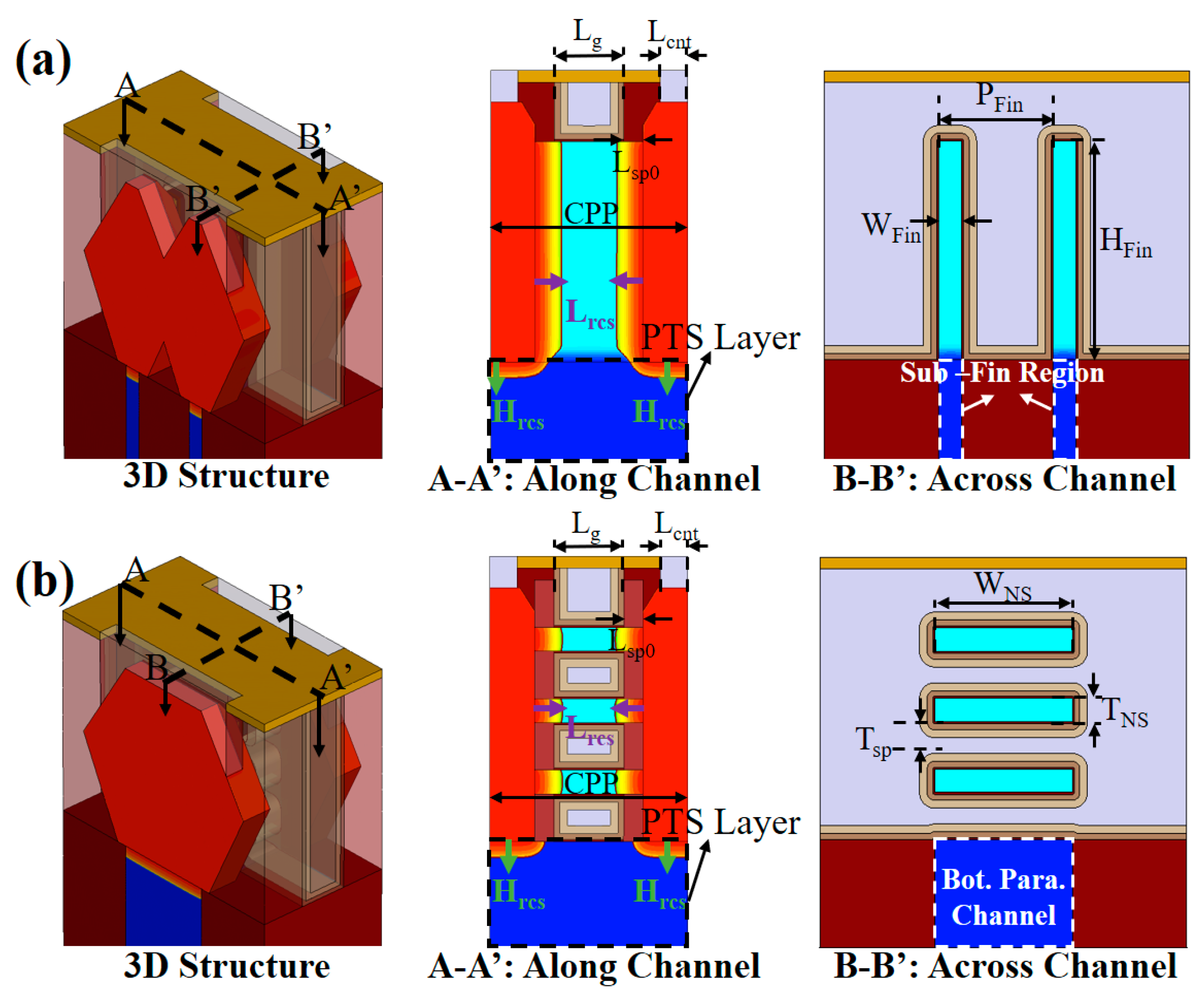
2. Device Structure and Simulation Methodology

3D schematics of the ideal 2-fin FinFET and 3-stacked NS FET structures are shown in Figure 1, with the lateral S/D recess distance Lrcs and the vertical S/D recess depth Hrcs labeled, respectively. Key device parameters of the studied Fin and NS FETs are summarized in Table 1 based on 5 nm node ground rules [26]. The gate length (Lg) of 18 nm, the spacer thickness (Lsp0) of 5 nm, and the contact gate pitch (CPP) of 51 nm are adopted. To ensure the same layout density, the active footprint of Fin and NS FETs is kept the same, namely the baseline GAA FET with 36 nm wide NS. The channel doping concentration is 1015/cm3 to avoid undesired carrier mobility degradation and the random doping fluctuation (RDF) [27]. In-situ and uniform doping S/D epitaxy was performed with 2 × 10²⁰/cm3 of phosphorus doping concentration for n-type MOS. The doping concentration of punch-through stopper (PTS) layer below the channel is 2 × 10¹⁸/cm3 to suppress the sub-Fin leakage [28]. As for the electrical characteristic simulations, the operating voltage (Vdd) is equal to 0.7 V, and the parasitic contact resistivity is fixed to 10−9 ohm·cm2 [29].
3D process simulations of Fin and NS FETs have been conducted using Sentaurus TCAD tools with advanced physical models [30]. A self-consistent calculation was achieved based on the drift-diffusion (DD) transport equation combined with the Poisson and carrier continuity equations. The bandgap narrowing effect dependent on the doping concentration was implemented by the Slotboom model in all the semiconductor regions [31]. Thinlayer and inversion and accumulation layer (IAL) mobility models were utilized, accounting for the impurity, phonon, surface roughness, and thin-layer-related scattering. Density-gradient (DG) based quantum correction models were included. Moreover, an auto-orientation framework was applied to take the surface orientation dependency of the carrier mobility and quantum correction into account. Ballistic mobility and high-field saturation models, Shockley-Read-Hall, Auger, and Hurkx band-to-band tunneling (BTBT) models were also included. The vital quantization effects, including quantum confinement and quantum tunneling, have been well implemented and considered in the TCAD simulation. By applying DG-based potential-like correction to the carrier density calculation formula, the carrier concentration deviates from the classical DD model and captures much quantum-mechanical behavior inside 3D device [32,33]. The BTBT tunneling current cannot be neglected if the electric field exceeds 7 × 10⁵ V/cm [34]. The Hurkx model is established based on the local variables and is conducive to numerical calculations. And these physical models have been utilized and validated in [13,23,35].
The physical model parameters have been delicately calibrated with the TSMC 7 nm node FinFET silicon data, as shown in Figure 2 [36]. The calibration process is performed as follows. The default physical model parameters are included in the material parameter file supplied by Synopsys, while some key process and physical model parameters are manually tuned within a reasonable range. Firstly, in the subthreshold regime, the doping profile is changed so that the TCAD simulation results can be well fitted to the experimental silicon data. As shown in Figure 2, the subthreshold swing (SS) and drain-induced barrier lowering (DIBL) are consistent with [36], which are ~64 mV/dec and ~30 mV/V, respectively. Furthermore, the ballistic coefficient and surface roughness scattering factor are tweaked to fit the Ids in the linear regime. The peak internal carrier saturation velocity of such scaling devices exceeds the conventional saturation velocity. In spite of this, the saturation velocity is increased from ~1.0 × 107 cm/s to ~3.0 × 107 cm/s in order to match the device on-state current. The final adjustment of saturation velocity is basically consistent with that reported in [35].
The transistor dimensions of the 5 nm technology node are not essentially different from those of the 7 nm node. Besides, the main transport surface orientation is changed from (110) of FinFET to (100) of NSFET. It has been well accounted for in the TCAD simulation through the auto-orientation framework based on the nearest interface. Therefore, the calibrated physical models can well apply to the 5 nm-node device electrical characterization in this work. As a matter of fact, with the continuous technology upgrading following Moore’s Law, the conventional pitch scaling has greatly slowed down and basically reached its limitation. This can be attributed to many reasons, such as lithography limitations, manufacturing costs, process variations, and stability. Instead, the chip performance boost becomes more reliable with the Design Technology Co-Optimization (DTCO) methodology to achieve equivalent scaling. Various techniques, including complementary FET (CFET), contact over active region (COAG), single diffusion break (SDB), buried power rail (BPR), and back-side power distribution network (BS-PDN), have been proposed [3,37,38]. They are mainly concerned with the improvement of power, performance, area and cost (PPAC) of the whole SoC design. Therefore, the physical models only need to be slightly tweaked for further scaling of the device on the condition that the related process parameters and device geometry are given correctly.

3. Results and Discussion

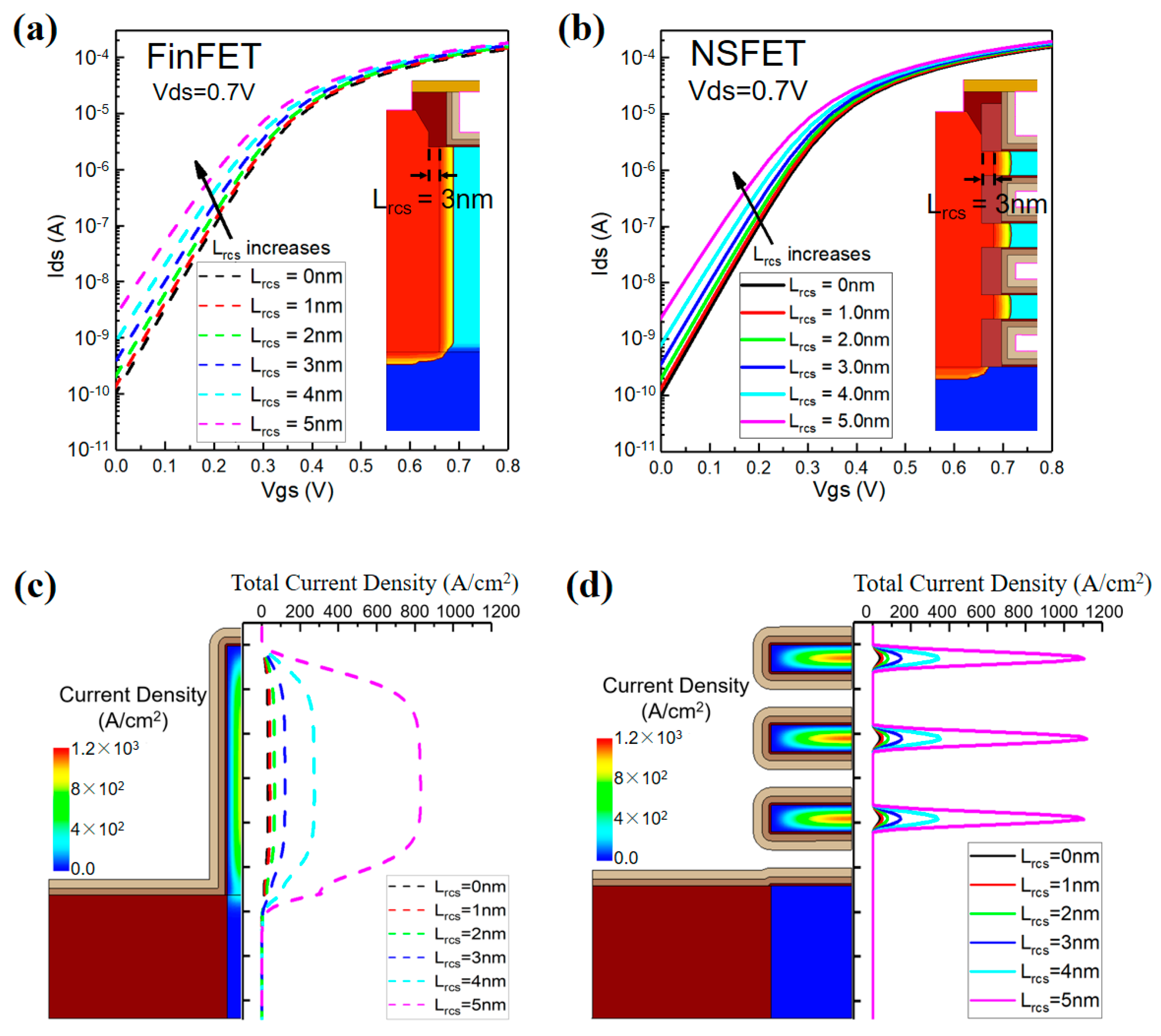
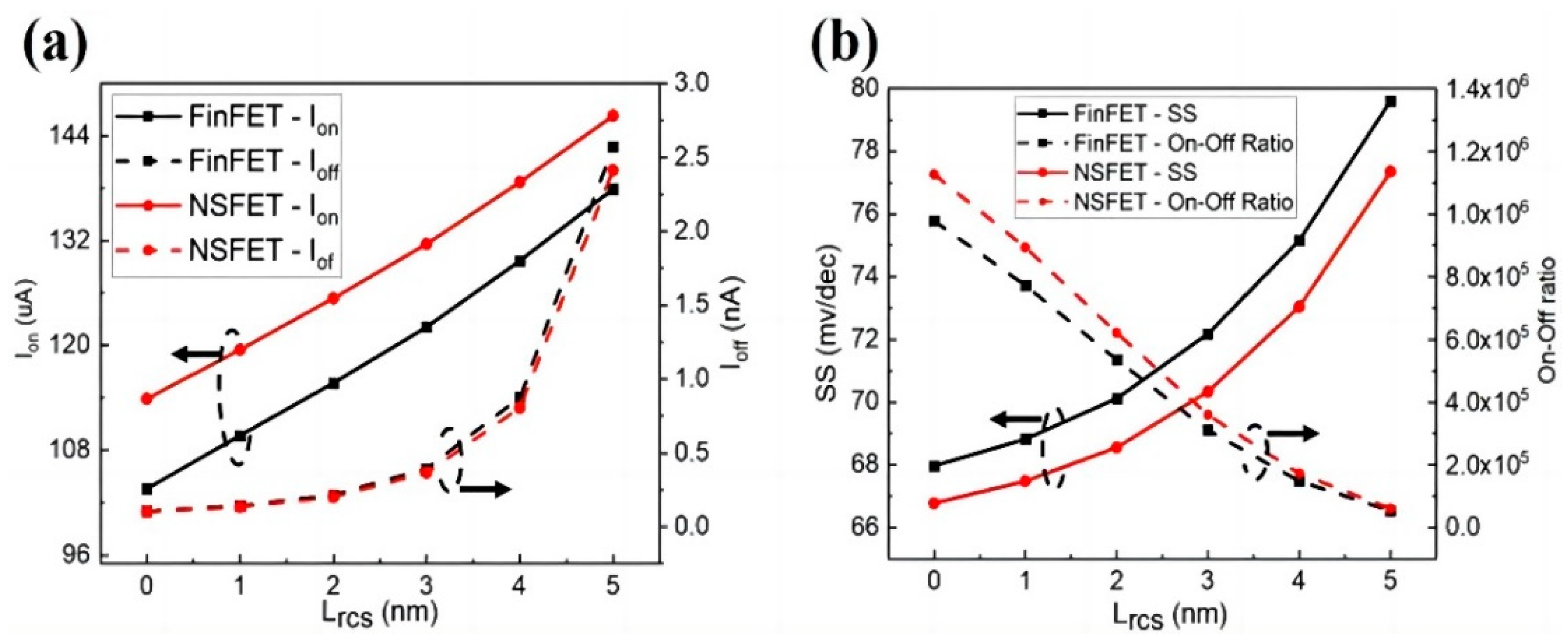
3.1. Lrcs Impacts on Device Performance

Figure 3 shows the transfer characteristics of both Fin and NS FETs with varied Lrcs. Low power (LP, Ioff = 0.1 nA) design is assumed for the work function (WF) modulation of Fin and NS FETs with ideal structures [23].
The upper limit of Lrcs is 5 nm, which is not larger than the spacer length in order to avoid channel damage. As the Lrcs increases, its impacts on both device types are almost the same, as shown in Figure 3a,b. While the on-state current (Ion) is elevated by additional Lrcs, the subthreshold characteristics such as the Ioff and SS deteriorate owing to the short channel effect (SCE). The Ioff of devices with Lrcs = 5.0 nm is more than 10 times larger than that of the ideal Fin and NS FETs. The device leakage current density profiles at 5 nm Lrcs are shown in Figure 3c,d, respectively. The higher current density peak value of the NSFET is compensated by its smaller cross-section and bottom parasitic channel leakage, so that the overall Ioff is still slightly smaller, as shown in Figure 4a. Furthermore, most of the off-state current resides in the intrinsic channel region, which indicates that the Isub dominates.
The key device characteristics, including the Ion, Ioff, SS, and on-off ratio, extracted from the Id-Vg curves are shown in Figure 4. Ion increases linearly as the epitaxial S/D region is brought closer to the channel with the exponential increase in the Ioff, whose increment is much more significant than Ion with increasing Lrcs. Compared with the FinFET, about 10% Ion improvement of the NSFET is obtained at the same footprint. It can be attributed to the fact that the effective width (Weff) of an NSFET with a 36 nm NS is 252 nm larger than that of a FinFET, which is 236 nm. The Weff of different device structures is calculated as shown in the following equations:
W e f f . F i n = ( 2 × H F i n + W F i n ) × F i n   N u m b e r
W e f f . N S = 2 × ( W N S + T N S ) × N S   N u m b e r
On the other hand, the electron transportation of NSFET is mainly implemented in the (100) orientation, in which the electron mobility is higher than that of the (110) surface orientation of FinFET [39]. The Ioff trends with varied Lrcs are almost the same for Fin and NS FETs, but the superior electrostatics of the NSFET is beneficial in suppressing the Isub. This result is consistent with the trends of SS shown in Figure 4b, which is a critical indicator of gate controllability. SS and on-off ratio simultaneously degrade with shorter effective gate lengths resulting from the larger Lrcs. In the meanwhile, better current drivability and effective suppression of the leakage current both contribute to the better on-off ratio of the NSFET.
Apart from DC behaviors, the AC performance also needs to be rigorously evaluated with the capacitance components taken into consideration. Firstly, LP design by WF tuning is considered so that the static power dissipation (Pstatic) is kept unchanged for different device structures. As shown in Figure 5a, the Ion at constant the Ioff shows differences from the absolute values shown in Figure 4a, of which the larger Lrcs also leads to more severe Ioff. Lrcs can be optimized to reduce the S/D extension region parasitic resistance with a reasonable gate controllability maintained so that the Ion is slightly boosted by ~3%. However, this DC gain brought by Lrcs will vanish if it is longer than 3 nm. The reason is that in this range, the deteriorative subthreshold characteristics will require a higher threshold voltage (Vth) to meet the needs of the LP design, and the on-state current will be negatively affected due to the overdrive voltage decrease (Vod). The trade-off between SCE immunity and device drivability should be carefully considered for device design and optimization.
Figure 5b shows the intrinsic and main parasitic capacitance components in the NSFET, of which the Cov,ISP between S/D and metal gate region is a specific element compared with the FinFET [8,10]. As the S/D is closer to each other through S/D lateral recess, the total gate capacitance (Cgg), including the parasitic components such as inner fringing (Cif), outer fringing (Cof) and overlap (Cov) capacitances, increases, as shown in Figure 5c. The intrinsic device RC delay is taken to evaluate the device AC performance and is defined as follows:
R C   D e l a y = V d d × C g g I o n
As shown in Figure 5a, the NS FET RC delay improvement over the FinFET is reduced to ~4.5% due to the larger parasitic capacitances. For both device types, the AC performance gain is adversely affected by increased Cgg, and the best RC delay improvement is reduced to ~1.5% with the optimal Lrcs shifted to the smaller value. The potential optimization of DC/AC performance at the constant Ioff can be achieved through the careful control of S/D lateral recess, but this improvement is limited due to the extremely scaled device dimensions of the 5 nm node. When Lrcs exceeds 3 nm, the gate control is more vulnerable, and the device performance will degrade rapidly.

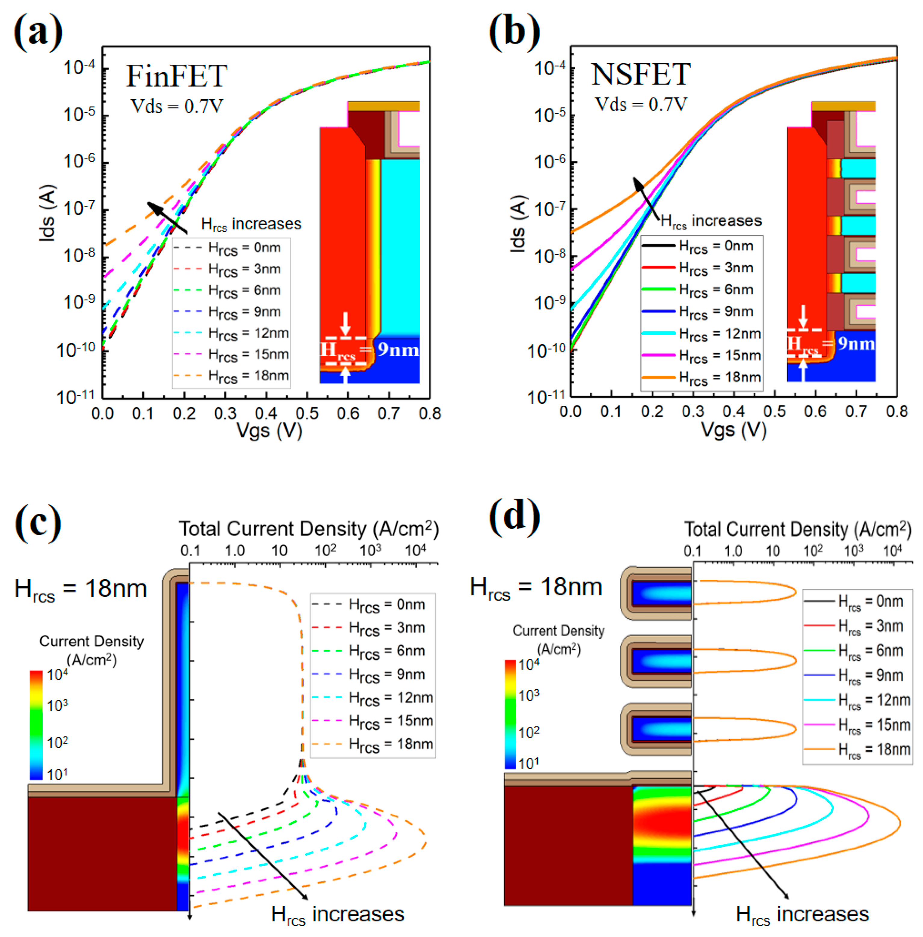
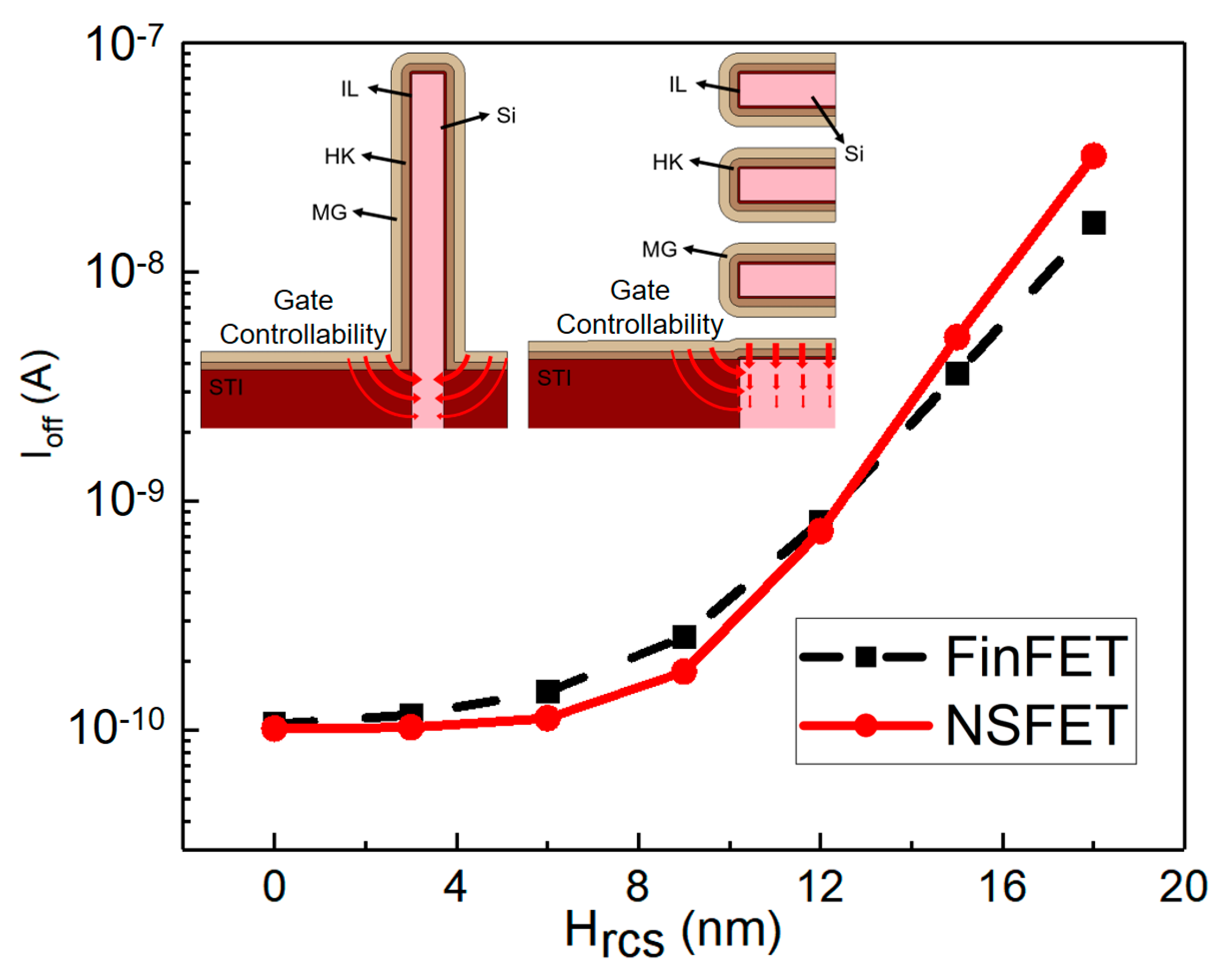
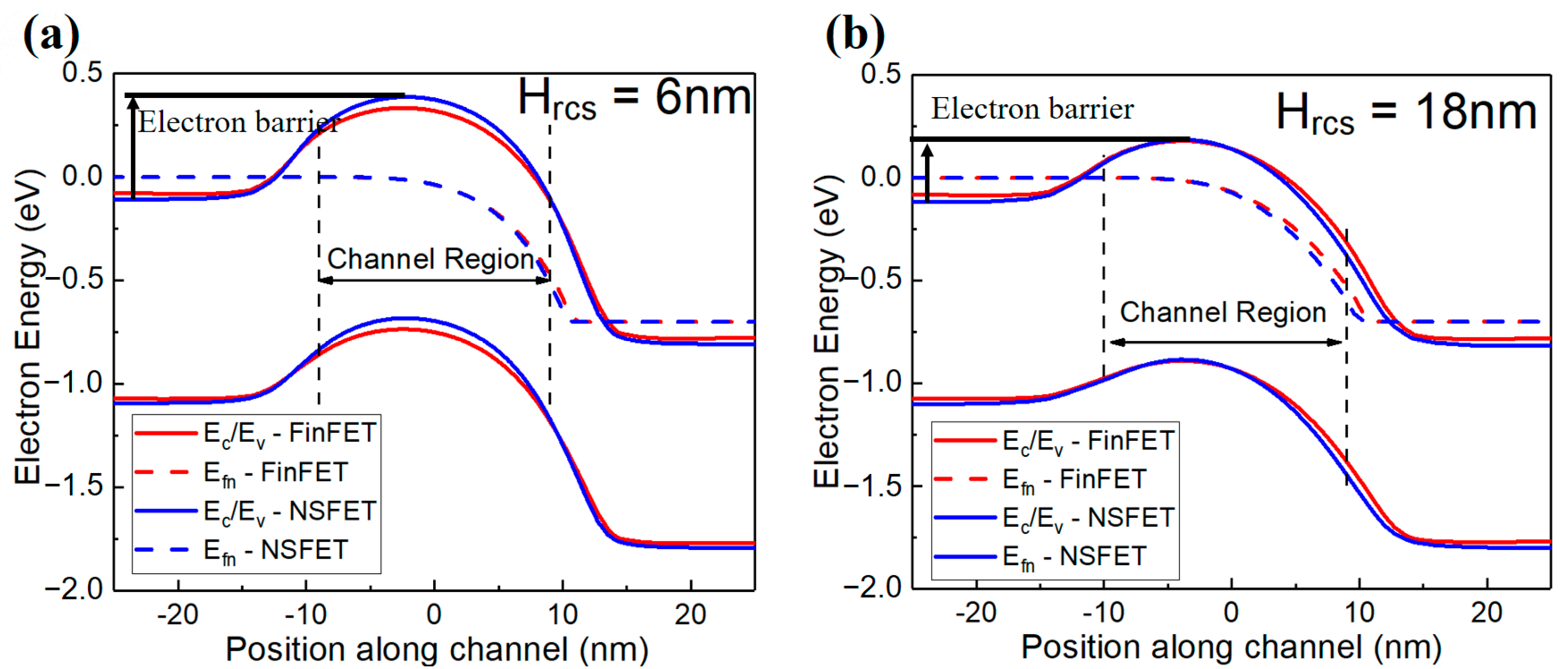
3.2. Hrcs Impacts on Device Performance

Furthermore, the impacts of the vertical S/D over recess variation have also been studied. The S/D region is heavily doped to minimize the parasitic resistance so that the depletion region mainly extends into the substrate. The extremely short Lg length of 18 nm leads to the significant proximity of the drain-substrate and the source-substrate depletion regions. Combining the factor that the drain is biased at Vdd in the off state, which will further widen the drain-substrate depletion region, the punch-through leakage path can be easily formed where the gate control is weak. Its increase will degrade the static power dissipation and the switching characteristics and should be suppressed as low as possible. Therefore, its impacts on the leakage current of Fin and NS FETs need to be quantitatively examined. Figure 6a,b shows the transfer characteristic curves for various Hrcs. The Ioff enormously increases when Hrcs exceeds 10 nm for both Fin and NS FETs.
If the vertical S/D recess is within good control, such as Hrcs = 0 nm, the subthreshold leakage through the channel dominates, as shown in Figure 3c,d. Due to higher PTS doping and a larger punch-through distance, the leakage through the sub-Fin or bottom parasitic channel is negligible. However, as shown in Figure 6c,d, when the Hrcs deviates from the ideal value (Hrcs = 0 nm), in addition to the subthreshold leakage by the channel, the IPT in the region far from the gate control will come into effect and increase rapidly while the leakage current in the channel region is barely affected. As Hrcs increases, more S/D dopants will undesirably diffuse in the sub-Fin or bottom parasitic channel region, leading to easier punch-through formation. The leakage path gets wider, and the peak current density is also increasing as its position shifts away from the surface.
The Ioff of various devices is extracted and presented in Figure 7. The Ioff of the NSFET is slightly smaller than that of the FinFET when Hrcs is relatively small. However, it will soon outperform the FinFET due to the wider bottom parasitic channel. As shown in Figure 7, the additional bottom gate still has more controllability than the FinFET over the region where punch-through leakage is formed. Therefore, when the Hrcs is relatively small, the increase in its punch-through current is not as sensitive as the FinFET. However, the Ioff of the NSFET will eventually exceed that of the FinFET as Hrcs increases because of the wider leakage path.
As shown in this Figure 8a, the electron barrier in the parasitic channel of NSFET is higher than that of FinFET due to the additional electrostatic control from the bottom gate electrode. The position of 0 nm corresponds to the center of the channel. Therefore, the source-to-drain leakage current of NSFET is 23% less than that of FinFET for 6 nm Hrcs. However, with the continuous increase in the Hrcs, the leakage path shifts away from the top of the STI, as shown in Figure 6c,d. In the meantime, more phosphorus inevitably diffuses into the Sub-Fin and the bottom parasitic channel region. This will make the effective substrate doping concentration (NA,eff) drop due to the doping compensation effect. The threshold voltage for these regions will decrease along with NA,eff reduction and bring about upsurge of the leakage current. The electron barriers of both devices decrease, as shown in Figure 8b, which indicates that these regions are easier to be affected by the S/D and the larger Ioff. Even though the electron barriers of Fin and NS FETs are almost the same at 18 nm Hrcs, the wider NS will take dominance over the additional bottom gate control effect and result in a larger device Ioff for the NSFET, as shown in Figure 7. This will reduce the device’s On-Off ratio more than 2 order and deteriorate the device switch characteristics.

3.3. S/D Recess Overall Impacts

The Ioff of Fin and NS FETs breaks down into 2 main components: the Isub in the channel region and the IPT in the sub-Fin or bottom parasitic channel region, as shown in Figure 9. 2 nm Lrcs and 10 nm Hrcs are assumed for S/D over recess in both directions. The 10 nm Hrcs is consistent with the values provided in ref. [20], which considers the process nonuniformity and variations. As mentioned above, the ideal Fin and NS FETs are designed to satisfy the LP requirement. In this case, the Isub takes up the most part, of which the portion is larger than 97%, while IPT is almost negligible. However, with lateral and vertical over recess happening in the device fabrication flow, both the Isub and IPT increase. Especially, the IPT becomes comparable to or even larger than the Isub for the devices with 2 nm Lrcs and 10 nm Hrcs. In this case, the Isub and IPT of the NSFET are less than those of the FinFET but are still under good control due to its superior gate electrostatics and additional gate control over the bottom parasitic channel region. With the above mentioned two main leakage components taken into consideration, the device overall leakage Ioff of NSFET is 37% less than that of FinFET. GAA’s superior leakage control capability is essential for its deployment in the mobile SoC of smartphones, in which scenario the low standby power design must be well addressed.

4. Conclusions

In this article, the DC and AC performances of FinFETs and GAA NSFETs with various S/D recess shapes are comprehensively investigated and compared using fully calibrated 3D TCAD simulations based on the 5 nm node dimensions. Device off-leakage is strongly related to the S/D lateral and vertical recesses. In terms of Lrcs, its increase will lead to a shorter Leff. This parameter, as a critical device parameter, can be optimized through Lrcs to achieve the best trade-off between SCE immunity and device drive capability for both Fin and GAA FETs. The simulation results show that the Ion can be enhanced by about ~3% while the RC delay, an important AC performance indicator, can be improved by ~1.5%. As for the 5 nm node dimensions, the electrostatic integrity is at risk, and the 18 nm Lg is approaching the scaling limitation. Therefore, it is more difficult to further reduce the Leff while keeping the SCE within an acceptable range. As a result, the DC and AC performance improvement is relatively small even at the optimal Lrcs. Regarding the vertical S/D recess, the Ioff of the NSFET is not as sensitive as that of the FinFET due to the additional bottom gate control when Hrcs can be well controlled under 12 nm. Beyond this range, the nature of the wider bottom parasitic channel of GAA NS FETs will come into dominance and exceed the leakage of FinFETs. With the presence of both Lrcs and Hrcs, the off-state current, including the Isub and IPT, of the NSFET is still under good control and exhibits 37% less Ioff than the FinFET. And the NSFET shows more robustness to the process variations, which is a critical factor in the next scaling node. Therefore, GAA NSFETs would provide better device performance and yield at the 5 nm technology node and beyond.

Author Contributions

Conceptualization, D.W.; methodology, D.W., T.L., K.C. and C.W.; investigation, D.W., X.S. and J.Y.; writing—original draft preparation, D.W.; writing—review and editing, T.L., C.W. and M.X.; supervision, W.Z. All authors have read and agreed to the published version of the manuscript.

Funding

This research received no external funding.

Data Availability Statement

The data and code are available from the corresponding authors upon reasonable request.

Acknowledgments

This work is sponsored by the platform for the development of next-generation integration circuit technology.

Conflicts of Interest

The authors declare no conflict of interest.

References

  1. Auth, C.; Allen, C.; Blattner, A.; Bergstrom, D.; Brazier, M.; Bost, M.; Buehler, M.; Chikarmane, V.; Ghani, T.; Glassman, T.; et al. A 22 nm high performance and low-power CMOS technology featuring fully-depleted tri-gate transistors, self-aligned contacts and high density MIM capacitors. In Proceedings of the 2012 Symposium on VLSI Technology (VLSIT), Honolulu, HI, USA, 12–14 June 2012; pp. 131–132. [Google Scholar]
  2. Natarajan, S.; Agostinelli, M.; Akbar, S.; Bost, M.; Bowonder, A.; Chikarmane, V.; Chouksey, S.; Dasgupta, A.; Fischer, K.; Fu, Q.; et al. A 14 nm logic technology featuring 2nd-generation FinFET, air-gapped interconnects, self-aligned double patterning and a 0.0588 µm2 SRAM cell size. In Proceedings of the 2014 IEEE International Electron Devices Meeting, San Francisco, CA, USA, 15–17 December 2014; pp. 71–73. [Google Scholar]
  3. Auth, C.; Aliyarukunju, A.; Asoro, M.; Bergstrom, D.; Bhagwat, V.; Birdsall, J.; Bisnik, N.; Buehler, M.; Chikarmane, V.; Ding, G.; et al. A 10nm high performance and low-power CMOS technology featuring 3rd generation FinFET transistors, self-aligned quad patterning, contact over active gate and cobalt local interconnects. In Proceedings of the 2017 IEEE International Electron Devices Meeting (IEDM), San Francisco, CA, USA, 2–6 December 2017; pp. 673–676. [Google Scholar]
  4. Wen, T.Y.; Colombeau, B.; Li, C.I.; Liu, S.Y.; Guo, B.N.; Meer, H.V.; Hou, M.; Yang, B.; Feng, H.C.; Hsu, C.F.; et al. Fin Bending Mitigation and Local Layout Effect Alleviation in Advanced FinFET Technology through Material Engineering and Metrology Optimization. In Proceedings of the 2019 Symposium on VLSI Technology, Kyoto, Japan, 9–14 June 2019. [Google Scholar]
  5. Razavieh, A.; Zeitzoff, P.; Nowak, E.J. Challenges and Limitations of CMOS Scaling for FinFET and Beyond Architectures. IEEE Trans. Nanotechnol. 2019, 18, 999–1004. [Google Scholar] [CrossRef]
  6. Loubet, N.; Hook, T.; Montanini, P.; Yeung, C.-W.; Kanakasabapathy, S.; Guillorn, M.; Yamashita, T.; Zhang, J.; Miao, X.; Wang, J.; et al. Stacked nanosheet gate-all-around transistor to enable scaling beyond FinFET. In Proceedings of the 2017 Symposium on VLSI Technology, Kyoto, Japan, 5–8 June 2017; pp. T230–T231. [Google Scholar]
  7. Mertens, H.; Ritzenthaler, R.; Chasin, A.; Schram, T.; Kunnen, E.; Hikavyy, A.; Ragnarsson, L.-Å.; Dekkers, H.; Hopf, T.; Wostyn, K.; et al. Vertically stacked gate-all-around Si nanowire CMOS transistors with dual work function metal gates. In Proceedings of the 2016 IEEE International Electron Devices Meeting (IEDM), San Francisco, CA, USA, 3–7 December 2016; pp. 19.17.11–19.17.14. [Google Scholar]
  8. Jang, D.; Yakimets, D.; Eneman, G.; Schuddinck, P.; Bardon, M.G.; Raghavan, P.; Spessot, A.; Verkest, D.; Mocuta, A. Device Exploration of NanoSheet Transistors for Sub-7-nm Technology Node. IEEE Trans. Electron Devices 2017, 64, 2707–2713. [Google Scholar] [CrossRef]
  9. Song, T.; Kim, H.; Rim, W.; Jung, H.; Park, C.; Lee, I.; Baek, S.; Jung, J. A 3-nm Gate-All-Around SRAM Featuring an Adaptive Dual-Bitline and an Adaptive Cell-Power Assist Circuit. IEEE J. Solid-State Circuits 2022, 57, 236–244. [Google Scholar] [CrossRef]
  10. Kim, S.; Kim, M.; Ryu, D.; Lee, K.; Kim, S.; Lee, J.; Lee, R.; Kim, S.; Lee, J.-H.; Park, B.-G. Investigation of Electrical Characteristic Behavior Induced by Channel-Release Process in Stacked Nanosheet Gate-All-Around MOSFETs. IEEE Trans. Electron Devices 2020, 67, 2648–2652. [Google Scholar] [CrossRef]
  11. Vincent, B.; Hathwar, R.; Kamon, M.; Ervin, J.; Schram, T.; Chiarella, T.; Demuynck, S.; Baudot, S.; Siew, Y.K.; Kubicek, S.; et al. Process Variation Analysis of Device Performance Using Virtual Fabrication: Methodology Demonstrated on a CMOS 14-nm FinFET Vehicle. IEEE Trans. Electron Devices 2020, 67, 5374–5380. [Google Scholar] [CrossRef]
  12. Rezali, F.A.M.; Othman, N.A.F.; Mazhar, M.; Hatta, S.W.M.; Soin, N. Performance and Device Design Based on Geometry and Process Considerations for 14/16-nm Strained FinFETs. IEEE Trans. Electron Devices 2016, 63, 974–981. [Google Scholar] [CrossRef]
  13. Kim, S.; Lee, K.; Kim, S.; Kim, M.; Lee, J.-H.; Kim, S.; Park, B.-G. Investigation of Device Performance for Fin Angle Optimization in FinFET and Gate-All-Around FETs for 3 nm-Node and Beyond. IEEE Trans. Electron Devices 2022, 69, 2088–2093. [Google Scholar] [CrossRef]
  14. Kranti, A.; Armstrong, G.A. Optimization of the source/drain extension region profile for suppression of short channel effects in sub-50 nm DG MOSFETs with high-κ gate dielectrics. Semicond. Sci. Technol. 2006, 21, 1563–1572. [Google Scholar] [CrossRef]
  15. Kranti, A.; Armstrong, G.A. Engineering source/drain extension regions in nanoscale double gate (DG) SOI MOSFETs: Analytical model and design considerations. Solid-State Electron. 2006, 50, 437–447. [Google Scholar] [CrossRef]
  16. Yang, J.-W.; Pham, D.; Zeitzoff, P.; Huff, H.; Brown, G. Optimization of Source/Drain Extension for Robust Speed Performance to Process Variation in Undoped Double-Gate CMOS. In Proceedings of the International Symposium on VLSI Technology, Systems, and Applications, Hsinchu, Taiwan, 24–26 April 2006; pp. 1–2. [Google Scholar]
  17. Jeong, J.; Yoon, J.-S.; Lee, S.; Baek, R.-H. Comprehensive Analysis of Source and Drain Recess Depth Variations on Silicon Nanosheet FETs for Sub 5-nm Node SoC Application. IEEE Access 2020, 8, 35873–35881. [Google Scholar] [CrossRef]
  18. Barraud, S.; Previtali, B.; Lapras, V.; Vizioz, C.; Hartmann, J.-M.; Martinie, S.; Lacord, J.; Cassé, M.; Dourthe, L.; Loup, V.; et al. Tunability of Parasitic Channel in Gate-All-Around Stacked Nanosheets. In Proceedings of the 2018 IEEE International Electron Devices Meeting (IEDM), San Francisco, CA, USA, 1–5 December 2018; pp. 21.23.21–21.23.24. [Google Scholar]
  19. Gu, J.; Zhang, Q.; Wu, Z.; Luo, Y.; Cao, L.; Cai, Y.; Yao, J.; Zhang, Z.; Xu, G.; Yin, H.; et al. Narrow Sub-Fin Technique for Suppressing Parasitic-Channel Effect in Stacked Nanosheet Transistors. IEEE J. Electron Devices Soc. 2022, 10, 35–39. [Google Scholar] [CrossRef]
  20. Zhang, J.; Frougier, J.; Greene, A.; Miao, X.; Yu, L.; Vega, R.; Montanini, P.; Durfee, C.; Gaul, A.; Pancharatnam, S.; et al. Full Bottom Dielectric Isolation to Enable Stacked Nanosheet Transistor for Low Power and High Performance Applications. In Proceedings of the 2019 IEEE International Electron Devices Meeting (IEDM), San Francisco, CA, USA, 7–11 December 2019; pp. 11.16.11–11.16.14. [Google Scholar]
  21. Wu, Y.-S.; Tsai, C.-H.; Miyashita, T.; Chen, P.-N.; Hsu, B.-C.; Wu, P.-H.; Hsu, H.-H.; Chiang, C.-Y.; Liu, H.-H.; Yang, H.-L.; et al. Optimization of fin profile and implant in bulk FinFET technology. In Proceedings of the International Symposium on VLSI Technology, Systems and Application (VLSI-TSA), Hsinchu, Taiwan, 25–27 April 2016; pp. 1–2. [Google Scholar]
  22. Wu, H.; Seo, S.-C.; Niu, C.; Wang, W.; Tsutsui, G.; Gluschenkov, O.; Liu, Z.; Petrescu, A.; Carr, A.; Choi, S.; et al. Integrated dual SPE processes with low contact resistivity for future CMOS technologies. In Proceedings of the 2017 IEEE International Electron Devices Meeting (IEDM), San Francisco, CA, USA, 2–6 December 2017; pp. 22.23.21–22.23.24. [Google Scholar]
  23. Yoon, J.-S.; Lee, S.; Lee, J.; Jeong, J.; Yun, H.; Kang, B.; Baek, R.-H. Source/Drain Patterning FinFETs as Solution for Physical Area Scaling Toward 5-nm Node. IEEE Access 2019, 7, 172290–172295. [Google Scholar] [CrossRef]
  24. Lee, J.; Yoon, J.-S.; Lee, S.; Jeong, J.; Baek, R.-H. TCAD-Based Flexible Fin Pitch Design for 3-nm Node 6T-SRAM Using Practical Source/Drain Patterning Scheme. IEEE Trans. Electron Devices 2021, 68, 1031–1036. [Google Scholar] [CrossRef]
  25. Roy, K.; Mukhopadhyay, S.; Mahmoodi-Meimand, H. Leakage current mechanisms and leakage reduction techniques in deep-submicrometer CMOS circuits. Proc. IEEE 2003, 91, 305–327. [Google Scholar] [CrossRef]
  26. IRDS. International Roadmap for Devices and Systems 2020 (IRDS 2020). Available online: https://irds.ieee.org/ (accessed on 31 July 2021).
  27. Wang, L.; Brown, A.; Cheng, B.; Asenov, A. Simulation of 3D FinFET doping profiles introduced by ion implantation and the impact on device performance. In Proceedings of the 20th International Conference on Ion Implantation Technology (IIT), Portland, OR, USA, 26 June–4 July 2014; pp. 1–4. [Google Scholar]
  28. Eneman, G.; Hellings, G.; Keersgieter, A.D.; Collaert, N.; Thean, A. Quantum-barriers and ground-plane isolation: A path for scaling bulk-FinFET technologies to the 7 nm-node and beyond. In Proceedings of the 2013 IEEE International Electron Devices Meeting, Washington, DC, USA, 9–11 December 2013; pp. 12.13.11–12.13.14. [Google Scholar]
  29. Wu, H.; Gluschenkov, O.; Tsutsui, G.; Niu, C.; Brew, K.; Durfee, C.; Prindle, C.; Kamineni, V.; Mochizuki, S.; Lavoie, C.; et al. Parasitic Resistance Reduction Strategies for Advanced CMOS FinFETs Beyond 7 nm. In Proceedings of the 2018 IEEE International Electron Devices Meeting (IEDM), San Francisco, CA, USA, 1–5 December 2018; pp. 35.34.31–35.34.34. [Google Scholar]
  30. Synopsys, Inc. TCAD Sentaurus Device User Guide; Synopsys Inc.: Mountain View, CA, USA, 2020. [Google Scholar]
  31. Klaassen, D.B.M.; Slotboom, J.W.; Graaff, H.C.D. Unified apparent bandgap narrowing in n- and p-type silicon. Solid-State Electron. 1992, 35, 125–129. [Google Scholar] [CrossRef]
  32. Ancona, M.G.; Tiersten, H.F. Macroscopic physics of the silicon inversion layer. Phys. Rev. B 1987, 35, 7959–7965. [Google Scholar] [CrossRef]
  33. Ancona, M.G.; Iafrate, G.J. Quantum correction to the equation of state of an electron gas in a semiconductor. Phys. Rev. B 1989, 39, 9536–9540. [Google Scholar] [CrossRef]
  34. Hurkx, G.A.M.; Klaassen, D.B.M.; Knuvers, M.P.G. A new recombination model for device simulation including tunneling. IEEE Trans. Electron Devices 1992, 39, 331–338. [Google Scholar] [CrossRef]
  35. Oldiges, P.; Vega, R.A.; Utomo, H.K.; Lanzillo, N.A.; Wassick, T.; Li, J.; Wang, J.; Shahidi, G.G. Chip Power-Frequency Scaling in 10/7 nm Node. IEEE Access 2020, 8, 154329–154337. [Google Scholar] [CrossRef]
  36. Wu, S.-Y.; Lin, C.Y.; Chiang, M.C.; Liaw, J.J.; Cheng, J.Y.; Chang, C.H.; Chang, V.S.; Pan, K.H.; Tsai, C.H.; Yao, C.H.; et al. Demonstration of a sub-0.03 um2 High Density 6-T SRAM with Scaled Bulk FinFETs for Mobile SOC Applications Beyond 10 nm Node. In Proceedings of the 2016 IEEE Symposium on VLSI Technology, Honolulu, HI, USA, 14–16 June 2016; pp. 1–2. [Google Scholar]
  37. Gupta, M.K.; Weckx, P.; Schuddinck, P.; Jang, D.; Chehab, B.; Cosemans, S.; Ryckaert, J.; Dehaene, W. A Comprehensive Study of Nanosheet and Forksheet SRAM for Beyond N5 Node. IEEE Trans. Electron Devices 2021, 68, 3819–3825. [Google Scholar] [CrossRef]
  38. Nibhanupudi, S.S.T.; Prasad, D.; Das, S.; Zografos, O.; Robinson, A.; Gupta, A.; Spessot, A.; Debacker, P.; Verkest, D.; Ryckaert, J.; et al. A Holistic Evaluation of Buried Power Rails and Back-Side Power for Sub-5 nm Technology Nodes. IEEE Trans. Electron Devices 2022, 69, 4453–4459. [Google Scholar] [CrossRef]
  39. Yoon, J.-S.; Jeong, J.; Lee, S.; Baek, R.-H. Systematic DC/AC Performance Benchmarking of Sub-7-nm Node FinFETs and Nanosheet FETs. IEEE J. Electron Devices Soc. 2018, 6, 942–947. [Google Scholar] [CrossRef]
Figure 1. 3D schematic view of the ideal device structure and 2D cross-sections across and along the channel of (a) FinFET and (b) NSFET with the same footprint.
Electronics 12 00770 g001
Figure 2. Physical model parameters calibrated to the mature 7 nm node Si-FinFET experimental data. Inset: Key geometry parameters of the fit device, of which the related parameters in the TCAD simulation is the same as [36].
Electronics 12 00770 g002
Figure 3. Id-Vg curves @ Vds = 0.7 V of (a) FinFET and (b) NSFET. Inset: Fin and NS FET devices with 3 nm Lrcs. Leakage current density profiles (Vgs = 0 V and Vds = 0.7 V) of (c) FinFET and (d) NSFET at 5 nm Lrcs.
Electronics 12 00770 g003
Figure 4. Trends of DC characteristics by Lrcs variations (a) Ion and Ioff, (b) SS and On-Off ratio.
Electronics 12 00770 g004
Figure 5. (a) Ion and RC Delay comparison at fixed Ioff with varied Lrcs (b) Schematic of intrinsic and parasitic gate capacitance components distribution in NSFET (c) Cgg trends by varying Lrcs for Fin and NS FETs.
Electronics 12 00770 g005
Figure 6. (a) Id-Vg curves @ Vds = 0.7V with various Hrcs from 0 nm to 18 nm for (a) Fin and (b) NS FETs. Leakage current density contour plots at Hrcs = 18 nm and its variation along Fin height direction of (c) Fin and (d) NS FETs.
Electronics 12 00770 g006
Figure 7. Ioff of Fin and NS FETs as a function of Hrcs. Inset: Gate controllability demonstration of sub-Fin region and bottom parasitic channel.
Electronics 12 00770 g007
Figure 8. Off-state electron energy band distribution along the channel direction at (a) 3 nm (1/2 × 6 nm) and (b) 9 nm (1/2 × 18 nm) below the shallow trench isolation (STI) respectively.
Electronics 12 00770 g008
Figure 9. Shows that the Ion and its main components of Fin and NS FETs with various structures.
Electronics 12 00770 g009
Table 1. Key Device Parameters for 5 nm Node Fin and NS FETs.
ParametersValue
BothContact gate pitch (CPP)51 nm
Gate length (Lg)18 nm
Spacer length (Lsp0)5 nm
Contact length (Lcnt)14 nm
S/D doping (Nsd)2 × 1020 cm−3
Channel Doping (Nch)1 × 1015 cm−3
Punch-Through Stop Doping (NPTS)2 × 1018 cm−3
FinNumber of Fin2
Fin width (WFin)6 nm
Fin height (HFin)56 nm
Fin pitch (PFin)30 nm
GAANumber of Nanosheet3
NS width (WNS)36 nm
NS Thickness (TNS)6 nm
NS Spacing (Tsp)12 nm
Disclaimer/Publisher’s Note: The statements, opinions and data contained in all publications are solely those of the individual author(s) and contributor(s) and not of MDPI and/or the editor(s). MDPI and/or the editor(s) disclaim responsibility for any injury to people or property resulting from any ideas, methods, instructions or products referred to in the content.

